AD5390/AD5391/AD5392 8-/16-Channel, 3 V/5 V, Serial Input, Single-Supply, 12-/14-Bit Voltage Output Data Sheet (Rev. B)
8-/16-Channel, 3 V/5 V, Serial Input,
Single-Supply, 12-/14-Bit Voltage Output
AD5390/AD5391/AD5392
Rev. B
Information furnished by Analog Devices is believed to be accurate and reliable. However, no
responsibility is assumed by Analog Devices for its use, nor for any infringements of patents or other
rights of third parties that may result from its use. Specifications subject to change without notice. No
license is granted by implication or otherwise under any patent or patent rights of Analog Devices.
Trademarks and registered trademarks are the property of their respective owners.
One Technology Way, P.O. Box 9106, Norwood, MA 02062-9106, U.S.A.
Tel: 781.329.4700
www.analog.com
Fax: 781.461.3113
©2006 Analog Devices, Inc. All rights reserved.
FEATURES
AD5390: 16-channel, 14-bit voltage output DAC
AD5391: 16-channel, 12-bit voltage output DAC
AD5392: 8-channel, 14-bit voltage output DAC
Guaranteed monotonic
INL
±1 LSB max (AD5391)
±3 LSB max (AD5390-5/AD5392-5)
±4 LSB max (AD5390-3/AD5392-3)
On-chip 1.25 V/2.5 V, 10 ppm/°C reference
Temperature range: -40°C to +85°C
Rail-to-rail output amplifier
Power-down mode
Package types
64-lead LFCSP (9 mm × 9 mm)
52-lead LQFP (10 mm × 10 mm)
User interfaces
Serial SPI
®
-, QSPI
TM
-, MICROWIRE
TM
-, and DSP-compatible
(featuring data readback)
I
2
C
®
-compatible interface
INTEGRATED FUNCTIONS
Channel monitor
Simultaneous output update via LDAC
Clear function to user-programmable code
Amplifier boost mode to optimize slew rate
User-programmable offset and gain adjust
Toggle mode enables square wave generation
Thermal monitor
APPLICATIONS
Instrumentation and industrial control
Power amplifier control
Level setting (ATE)
Control systems
Microelectromechanical systems (MEMs)
Variable optical attenuators (VOAs)
Optical transceivers (MSA 300, XFP)
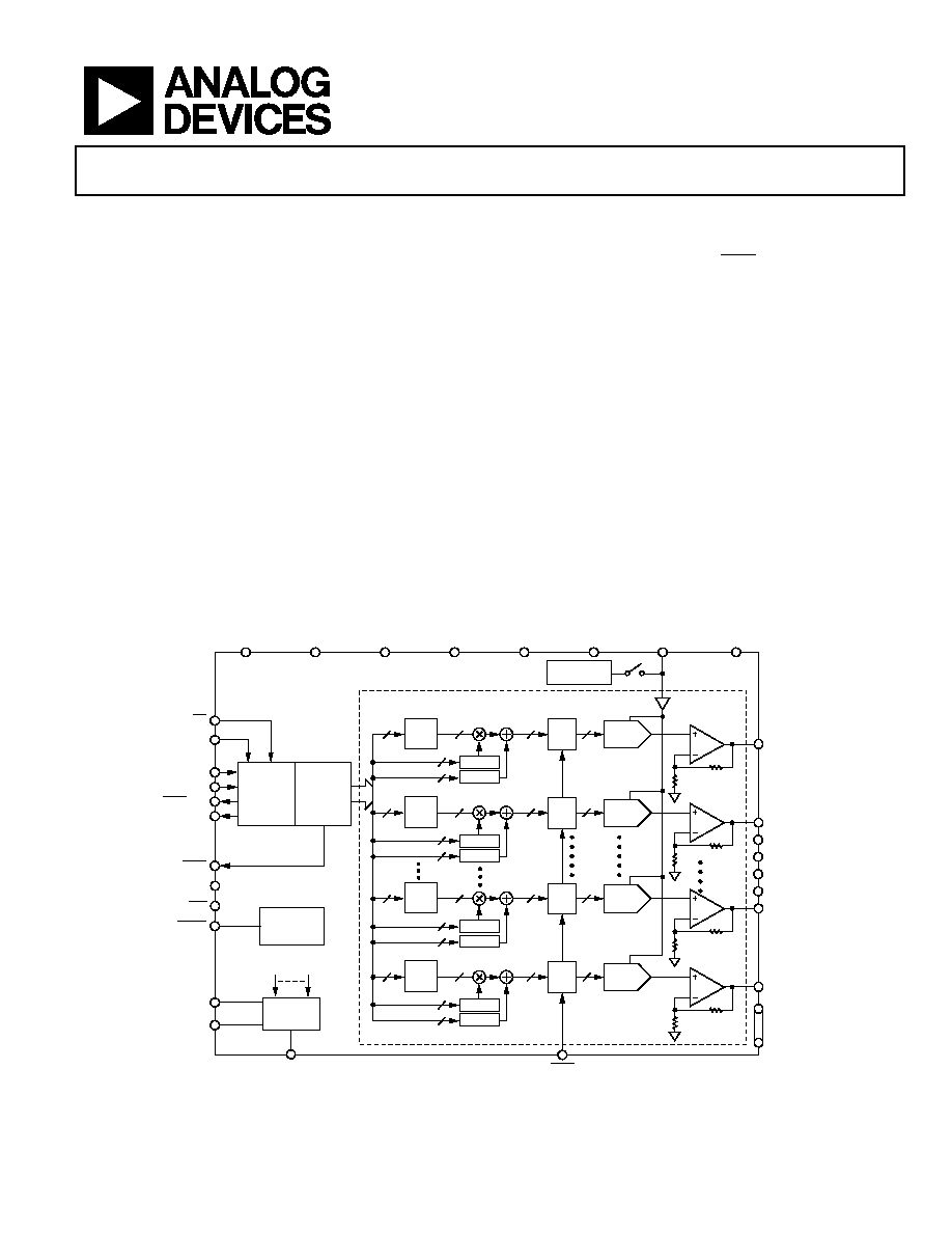
FUNCTIONAL BLOCK DIAGRAM
R
DAC 0
R
VOUT 0
DAC
REG
0
14
14
R
DAC 1
R
VOUT 1
VOUT 2
VOUT 3
VOUT 4
VOUT 5
DAC
REG
1
14
14
R
DAC 6
R
VOUT 6
DAC
REG
6
14
14
R
DAC 7
R
VOUT 7
VOUT 8
VOUT 15
DAC
REG
7
14
14
m REG0
c REG0
14
14
14
14
INPUT
REG
0
m REG1
c REG1
14
14
14
14
INPUT
REG
1
m REG6
c REG6
14
14
14
14
INPUT
REG
6
m REG7
c REG7
14
14
14
14
INPUT
REG
7
STATE
MACHINE
AND
CONTROL
LOGIC
INTERFACE
CONTROL
LOGIC
DIN/SDA
DCEN/AD1
SPI/I
2
C
SCLK/SCL
SYNC/AD0
SDO
1.25V/2.5V
REFERENCE
AD5390
REFOUT/REFIN SIGNAL_GND (×2)
REF_GND
DAC_GND (×2)
AGND (×2)
AV
DD
(×2)
DGND (×3/×4)
DV
DD
(×3)
×2
LDAC
POWER-ON
RESET
BUSY
PD
CLR
RESET
MON_IN1
MON_IN2
MON_OUT
V
IN
0
V
IN
15
MUX
03773-
001
Figure 1.
Rev. B
Information furnished by Analog Devices is believed to be accurate and reliable. However, no
responsibility is assumed by Analog Devices for its use, nor for any infringements of patents or other
rights of third parties that may result from its use. Specifications subject to change without notice. No
license is granted by implication or otherwise under any patent or patent rights of Analog Devices.
Trademarks and registered trademarks are the property of their respective owners.
One Technology Way, P.O. Box 9106, Norwood, MA 02062-9106, U.S.A.
Tel: 781.329.4700
www.analog.com
Fax: 781.461.3113
©2006 Analog Devices, Inc. All rights reserved.

AD5390/AD5391/AD5392
Rev. B | Page 2 of 44
TABLE OF CONTENTS
Features .............................................................................................. 1
Integrated Functions ........................................................................ 1
Applications....................................................................................... 1
Functional Block Diagram .............................................................. 1
Revision History ............................................................................... 2
General Description ......................................................................... 3
AD5390-5/AD5391-5/AD5392-5 Specifications.......................... 4
AD5390-5/AD5391-5/AD5392-5 AC Characteristics................. 6
AD5390-3/AD5391-3/AD5392-3 Specifications.......................... 7
AD5390-3/AD5391-3/AD5392-3 AC Characteristics................. 9
Timing Characteristics................................................................... 10
Serial SPI-, QSPI-, MICROWIRE-, and DSP-
Compatible Interface.................................................................. 10
I
2
C Serial Interface...................................................................... 12
Absolute Maximum Ratings.......................................................... 13
ESD Caution................................................................................ 13
Pin Configuraton and Function Descriptions ............................ 14
Terminology .................................................................................... 17
Typical Performance Characteristics ........................................... 18
Functional Description .................................................................. 22
DAC Architecture....................................................................... 22
Data Decoding ............................................................................ 23
Interfaces.......................................................................................... 24
DSP-, SPI-, and MICROWIRE-
Compatible Serial Interface ...................................................... 24
I
2
C Serial Interface ..................................................................... 26
I
2
C Write Operation ....................................................................... 27
4-Byte Mode................................................................................ 27
3-Byte Mode................................................................................ 28
2-Byte Mode................................................................................ 29
AD539x On-Chip Special Function Registers........................ 30
Control Register Write............................................................... 32
Hardware Functions....................................................................... 34
Reset Function ............................................................................ 34
Asynchronous Clear Function.................................................. 34
BUSY and LDAC Functions...................................................... 34
Power-On Reset.......................................................................... 34
Power-Down ............................................................................... 34
Microprocessor Interfacing....................................................... 34
Application Information................................................................ 36
Power Supply Decoupling ......................................................... 36
Typical Configuration Circuit .................................................. 36
AD539x Monitor Function ....................................................... 37
Toggle Mode Function............................................................... 37
Thermal Monitor Function....................................................... 37
Outline Dimensions ....................................................................... 39
Ordering Guide .......................................................................... 40
REVISION HISTORY
3/06--Rev. A to Rev. B
Changes to Figure 1.......................................................................... 1
Changes to Table 9.......................................................................... 14
Changes to Table 12 and Table 15 ................................................ 23
Updated Outline Dimensions ....................................................... 39
Changes to Ordering Guide .......................................................... 40
10/04--Rev. 0 to Rev. A
Changes to Features.......................................................................... 1
Changes to Table 1............................................................................ 3
Changes to Table 2............................................................................ 4
Changes to Table 3.............................................................................6
Changes to Table 4.............................................................................7
Changes to Figure 36...................................................................... 35
Changes to Figure 37...................................................................... 36
Changes to Figure 38...................................................................... 36
Changes to Ordering Guide .......................................................... 41
4/04--Revision 0: Initial Version
AD5390/AD5391/AD5392
Rev. B | Page 3 of 44
GENERAL DESCRIPTION
The AD5390/AD5391 are complete single-supply, 16-channel,
14-bit and 12-bit DACs, respectively. The AD5392 is a complete
single-supply, 8-channel, 14-bit DAC. The devices are available
in either a 64-lead LFCSP or a 52-lead LQFP. All channels have
an on-chip output amplifier with rail-to-rail operation. All
devices include an internal 1.25/2.5 V, 10 ppm/°C reference, an
on-chip channel monitor function that multiplexes the analog
outputs to a common MON_OUT pin for external monitoring,
and an output amplifier boost mode that optimizes the output
amplifier slew rate.
The AD5390/AD5391/AD5392 contain a 3-wire serial interface
with interface speeds in excess of 30 MHz that are compatible
with SPI, QSPI, MICROWIRE, and DSP interface standards
and an I
2
C-compatible interface supporting a 400 kHz data
transfer rate.
An input register followed by a DAC register provides double-
buffering, allowing DAC outputs to be updated independently
or simultaneously using the LDAC input. Each channel has a
programmable gain and offset adjust register, letting the user
fully calibrate any DAC channel.
Power consumption is typically 0.25 mA per channel.
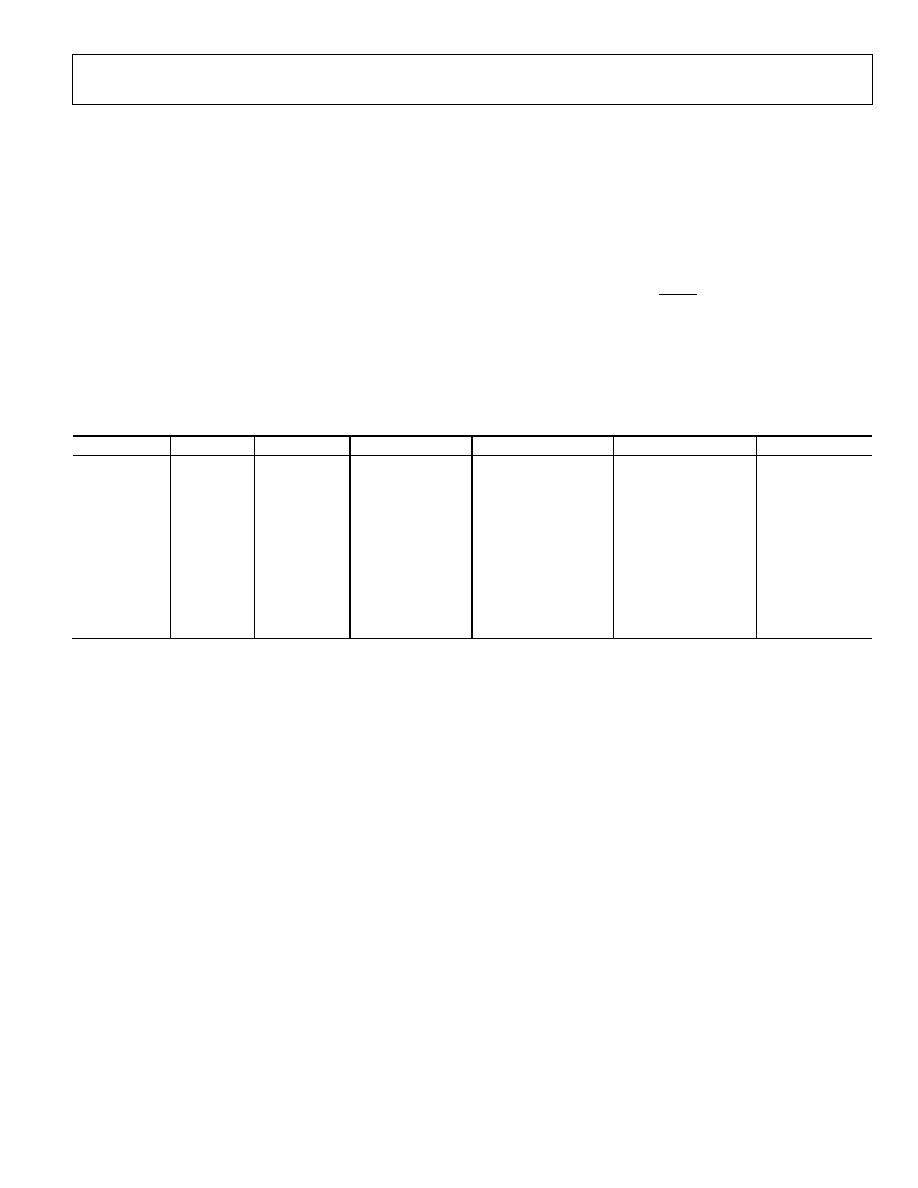
Table 1. Additional High Channel Count, Low Voltage, Single-Supply DACs in Portfolio
Model Resolution
AV
DD
Range
Output Channels
Linearity Error (LSB)
Package Description
Package Option
AD5380BST-5
14 Bits
4.5 V to 5.5 V
40
±4
100-Lead LQFP
ST-100
AD5380BST-3
14 Bits
2.7 V to 3.6 V
40
±4
100-Lead LQFP
ST-100
AD5384BBC-5
14 Bits
4.5 V to 5.5 V
40
±4
100-Lead CSPBGA
BC-100
AD5384BBC-3
14 Bits
2.7 V to 3.6 V
40
±4
100-Lead CSPBGA
BC-100
AD5381BST-5
12 Bits
4.5 V to 5.5 V
40
±1
100-Lead LQFP
ST-100
AD5381BST-3
12 Bits
2.7 V to 3.6 V
40
±1
100-Lead LQFP
ST-100
AD5382BST-5
14 Bits
4.5 V to 5.5 V
32
±4
100-Lead LQFP
ST-100
AD5382BST-3
14 Bits
2.7 V to 3.6 V
32
±4
100-Lead LQFP
ST-100
AD5383BST-5
12 Bits
4.5 V to 5.5 V
32
±1
100-Lead LQFP
ST-100
AD5383BST-3
12 Bits
2.7 V to 3.6 V
32
±1
100-Lead LQFP
ST-100

AD5390/AD5391/AD5392
Rev. B | Page 4 of 44
AD5390-5/AD5391-5/AD5392-5 SPECIFICATIONS
AV
DD
= 4.5 V to 5.5 V; DV
DD
= 2.7 V to 5.5 V; AGND = DGND = 0 V; REFIN = 2.5 V external. All specifications T
MIN
to T
MAX
,
unless otherwise noted.
Table 2.
Parameter
AD5390-5
1
AD5392-5
1
AD5391-5
1
Unit Test
Conditions/Comments
ACCURACY
Resolution 14
12
Bits
Relative Accuracy
±3
±1
LSB max
Differential Nonlinearity
-1/+2
±1
LSB max
Guaranteed monotonic over temperature
Zero-Scale Error
4
4
mV max
Offset Error
±4
±4
mV max
Measured at code 32 in the linear region
Offset Error TC
±5
±5
V/°C typ
Gain Error
±0.024
±0.024
% FSR max
At 25°C T
MIN
to T
MAX
±0.06
±0.06
% FSR max
Gain Temperature Coefficient
2
2
2
ppm FSR/°C typ
DC Crosstalk
2
0.5 0.5 LSB
max
REFERENCE INPUT/OUTPUT
Reference Input
2
Reference Input Voltage
2.5
2.5
V
±1% for specified performance,
AV
DD
= 2 × REFIN + 50 mV
DC Input Impedance
1
1
M min
Typically 100 M
Input Current
±1
±1
A max
Typically ±30 nA
Reference Range
1 V to
AV
DD
/2
1 V to AV
DD
/2 V
min/max
Reference Output
3
Enabled via internal/external bit in control
register; REF select bit in control register
selects the reference voltage
Output Voltage
2.495/2.505
2.495/2.505
V min/max
At ambient, optimized for 2.5 V operation
1.22/1.28
1.22/1.28
V min/max
At ambient when 1.25 V reference is selected
Reference TC
±10
±10
ppm max
Temperature range: 25°C to 85°C
±15
±15
ppm max
Temperature range: -40°C to +85°C
Output Impedance
2.2
2.2
k typ
OUTPUT CHARACTERISTICS
2
Output Voltage Range
4
0/AV
DD
0/AV
DD
V
min/max
Short-Circuit Current
40
40
mA max
Load Current
±1
±1
mA max
Capacitive Load Stability
R
L
=
200
200
pF max
R
L
= 5 k
1000
1000
pF max
DC Output Impedance
0.5
0.5
max
MONITOR OUTPUT PIN
Output Impedance
500
500
typ
Three-State Leakage Current
100
100
nA typ
LOGIC INPUTS
2
DV
DD
= 2.7 V to 5.5 V
V
IH
, Input High Voltage
2
2
V min
V
IL
, Input Low Voltage
0.8
0.8
V max
Input Current
±10
±10
A max
Total for all pins, T
A
= T
MIN
to T
MAX
Pin Capacitance
10
10
pF max

AD5390/AD5391/AD5392
Rev. B | Page 5 of 44
Parameter
AD5390-5
1
AD5392-5
1
AD5391-5
1
Unit Test
Conditions/Comments
LOGIC INPUTS (SCL, SDA Only)
V
IH
, Input High Voltage
0.7 DV
DD
0.7
DV
DD
V min
SMBus-compatible at DV
DD
< 3.6 V
V
IL
, Input Low Voltage
0.3 DV
DD
0.3
DV
DD
V max
SMBus-compatible at DV
DD
< 3.6 V
I
IN
, Input Leakage Current
±1
±1
A max
V
HYST
, Input Hysteresis
0.05 DV
DD
0.05
DV
DD
V
min
C
IN
, Input Capacitance
8
8
pF typ
Glitch Rejection
50
50
ns max
Input filtering suppresses noise spikes of <50 ns
LOGIC OUTPUTS (BUSY, SDO)
2
Output Low Voltage
0.4
0.4
V max
DV
DD
= 5 V ± 10%, sinking 200 A
Output High Voltage
DV
DD
- 1
DV
DD
- 1
V min
DV
DD
= 5 V ± 10%, SDO only, sourcing 200 A
Output Low Voltage
0.4
0.4
V max
DV
DD
= 2.7 V to 3.6 V, sinking 200 A
Output High Voltage
DV
DD
- 0.5
DV
DD
- 0.5
V min
DV
DD
= 2.7 V to 3.6 V SDO only, sourcing 200 A
High Impedance Leakage Current
±1
±1
A max
High Impedance Output Capacitance
5
5
pF typ
LOGIC OUTPUT (SDA)
2
V
OL
, Output Low Voltage
0.4
0.4
V max
I
SINK
= 3 mA
0.6
0.6
V
max
I
SINK
= 6 mA
Three-State Leakage Current
±1
±1
A max
Three-State Output Capacitance
8
8
pF typ
POWER REQUIREMENTS
AV
DD
4.5/5.5
4.5/5.5
V
min/max
DV
DD
2.7/5.5
2.7/5.5
V
min/max
Power Supply Sensitivity
2
Midscale/AV
DD
-85
-85
dB
typ
AI
DD
0.375
0.375
mA/channel
max
Outputs unloaded, boost off,
0.25 mA/channel typ
AI
DD
0.475
0.475
mA/channel
max
Outputs unloaded, boost on,
0.325 mA/channel typ
DI
DD
1
1
mA
max
V
IH
= DV
DD
, V
IL
= DGND
AI
DD
(Power-Down)
1
1
A max
Typically 200 nA
DI
DD
(Power-Down)
20
20
A max
Typically 3 A
Power Dissipation
35
35
mW max
AD5390/AD5391 with outputs unloaded,
AV
DD
= DV
DD
= 5 V, boost off
20
20
mW
max
AD5392 with outputs unloaded,
AV
DD
= DV
DD
= 5 V, boost off
1
AD539x-5 products are calibrated with a 2.5 V reference. Temperature range for all versions: -40°C to +85°C.
2
Guaranteed by characterization, not production tested.
3
Programmable either to 1.25 V typical or 2.5 V typical via the AD539x control register. Operating the AD539x-5 products with a reference of 1.25 V leads to a
degradation in performance accuracy.
4
Accuracy guaranteed from VOUT = 10 mV to AV
DD
- 50 mV.
Document Outline
- þÿ
- þÿ
- þÿ
- þÿ
- þÿ
- þÿ
- þÿ
- þÿ
- þÿ
- þÿ
- þÿ
- þÿ
- þÿ
- þÿ
- þÿ
- þÿ
- þÿ
- þÿ
- þÿ
- þÿ
- þÿ
- BUSY AND LDAC FUNCTIONS
- þÿ
- þÿ
- þÿ
- þÿ
- þÿ