Äîêóìåíòàöèÿ è îïèñàíèÿ www.docs.chipfind.ru
Dual 12-Bit, High Bandwidth, Multiplying DAC with
4-Quadrant Resistors and Parallel Interface
AD5405
Rev. 0
Information furnished by Analog Devices is believed to be accurate and reliable.
However, no responsibility is assumed by Analog Devices for its use, nor for any
infringements of patents or other rights of third parties that may result from its use.
Specifications subject to change without notice. No license is granted by implication
or otherwise under any patent or patent rights of Analog Devices. Trademarks and
registered trademarks are the property of their respective owners.
One Technology Way, P.O. Box 9106, Norwood, MA 02062-9106, U.S.A.
Tel: 781.329.4700
www.analog.com
Fax: 781.326.8703
© 2004 Analog Devices, Inc. All rights reserved.
FEATURES
On chip 4-quadrant resistors allow flexible output ranges
10 MHz multiplying bandwidth
Fast parallel interface write cycle: 58 MSPS
2.5 V to 5.5 V supply operation
±10 V reference input
Extended temperature range:
-40°C to 125°C
40-lead LFCSP package
Guaranteed monotonic
4-quadrant multiplication
Power-on reset
Readback function
.5 µA typical current consumption
APPLICATIONS
Portable battery-powered applications
Waveform generators
Analog processing
Instrumentation applications
Programmable amplifiers and attenuators
Digitally-controlled calibration
Programmable filters and oscillators
Composite video
Ultrasound
Gain, offset, and voltage trimming
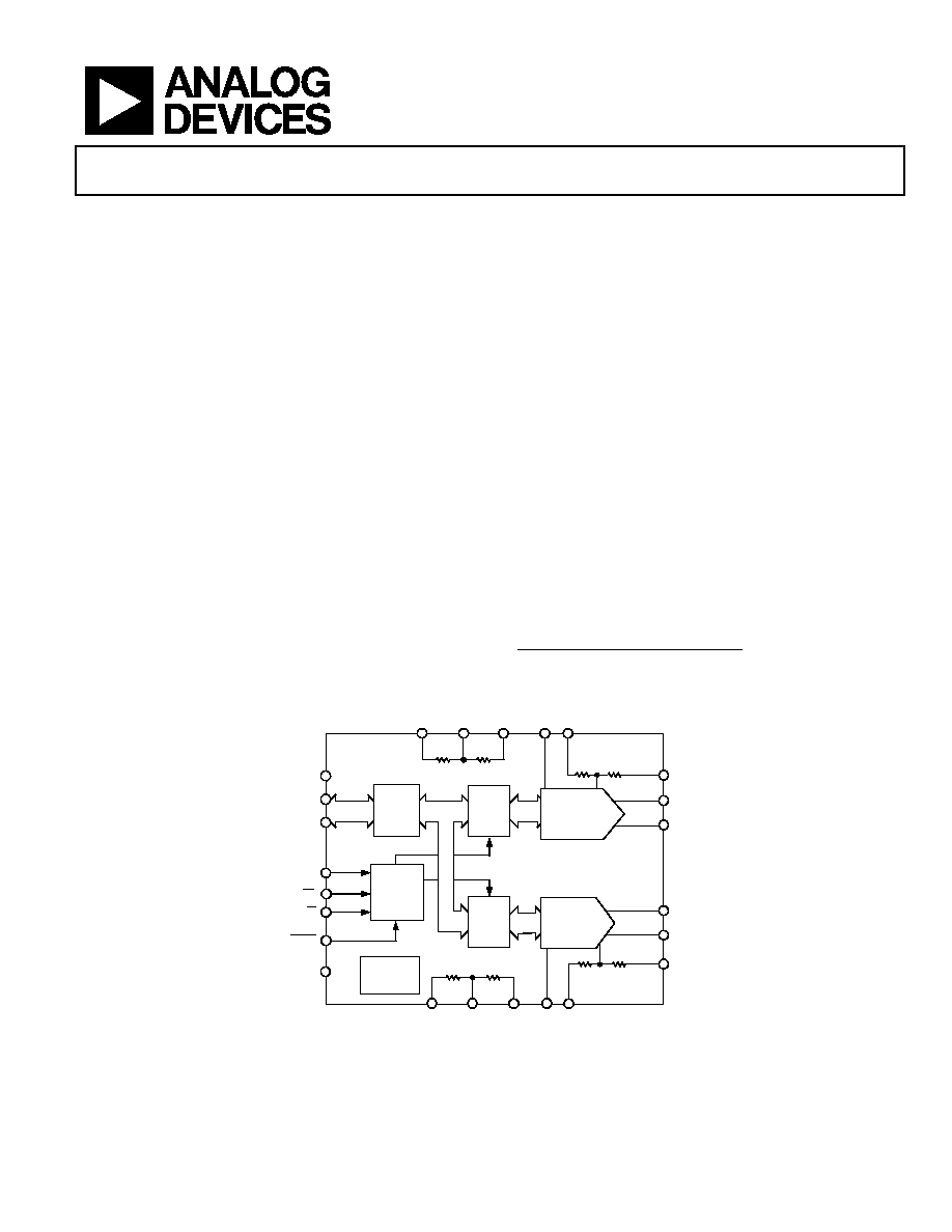
GENERAL DESCRIPTION
The AD5405
1
is a dual CMOS, 12-bit, current output digital-
to-analog converter (DAC).This device operates from a 2.5 V to
5.5 V power supply, making it suited to battery-powered and
other applications.
The applied external reference input voltage (V
REF
) determines
the full-scale output current. An integrated feedback resistor
(R
FB
) provides temperature tracking and full-scale voltage
output when combined with an external I-to-V precision
amplifier. This device also contains all the 4-quadrant resistors
necessary for bipolar operation and other configuration modes.
This DAC utilizes data readback, allowing the user to read the
contents of the DAC register via the DB pins. On power-up, the
internal register and latches are filled with zeros and the DAC
outputs are at zero scale.
As a result of manufacture with a CMOS submicron process, the
device offers excellent 4-quadrant multiplication characteristics,
with large signal multiplying bandwidths of up to 10 MHz.
The AD5405 has a 6 mm × 6 mm, 40-lead LFCSP package.
1
US Patent Number 5,689,257.
V
REF
A
AD5405
V
REF
B
V
DD
DB0
DB11
DATA
INPUTS
DAC A/B
CS
R/W
GND
CONTROL
LOGIC
INPUT
BUFFER
LATCH
I
OUT
1B
I
OUT
1A
12-BIT
R-2R DAC A
R
FB
A
POWER-ON
RESET
12-BIT
R-2R DAC B
LATCH
R1
2R
R1A
R2
2R
R3
2R
R3A
R2A
R2_3A
R2
2R
R3
2R
R3B
R2B
R2_3B
RFB
2R
R1
2R
RFB
2R
R1B
I
OUT
2A
I
OUT
2B
LDAC
04463-0-001
R
FB
B
Figure 1. AD5405 Functional Block Diagram

AD5405
Rev. 0 | Page 2 of 24
TABLE OF CONTENTS
Specifications..................................................................................... 3
Timing Characteristics..................................................................... 5
Absolute Maximum Ratings............................................................ 6
ESD Caution.................................................................................. 6
Pin Configuration and Function Descriptions............................. 7
Typical Performance Characteristics ............................................. 8
Terminology .................................................................................... 13
General Description ....................................................................... 14
DAC Section................................................................................ 14
Circuit Operation ....................................................................... 14
Single-Supply Applications........................................................ 15
Positive Output Voltage ............................................................. 15
Adding Gain................................................................................ 15
Used as a Divider or Programmable Gain Element............... 16
Reference Selection .................................................................... 16
Amplifier Selection .................................................................... 16
Parallel Interface......................................................................... 17
Microprocessor Interfacing....................................................... 17
PCB Layout and Power Supply Decoupling ........................... 17
Evaluation Board for the DACs................................................ 18
Overview of AD54xx Devices....................................................... 22
Outline Dimensions ....................................................................... 23
Ordering Guide .......................................................................... 23
REVISION HISTORY
7/04--Revision 0: Initial Version

AD5405
Rev. 0 | Page 3 of 24
SPECIFICATIONS
1
V
DD
= 2.5 V to 5.5 V, V
REF
A = V
REF
B = 10 V, I
OUT
2 = 0 V. All specifications T
MIN
to T
MAX,
unless otherwise noted. DC performance measured
with OP1177, AC performance with AD9631, unless otherwise noted.
Table 1.
Parameter Min
Typ
Max
Unit
Conditions
STATIC PERFORMANCE
Resolution
12
Bits
Relative Accuracy
±1
LSB
Differential Nonlinearity
-1/+2
LSB
Guaranteed monotonic
Gain Error
±25
mV
Gain Error Temp Coefficient
2
±5
ppm
FSR/°C
Bipolar Zero-Code Error
±25
mV
Output Leakage Current
±1
nA
Data = 0x0000, T
A
= 25°C, I
OUT
1
±10
nA
Data = 0x0000
H
, I
OUT
1
REFERENCE INPUT
2
Typical resistor TC =
-50 ppm/°C
Reference Input Range
±10
V
V
REF
A, V
REF
B Input Resistance
8
10
12
k
DAC input resistance
V
REF
A to V
REF
B Input Resistance
Mismatch
1.6
2.5
%
Typ = 25°C, Max = 125°C
R
1
, R
FB
Resistance
16
20
24
k
R
2
, R
3
Resistance
16
20
24
k
R
2
to R
3
Resistance Mismatch
.06
.18
%
Typ = 25°C, Max = 125°C
DIGITAL INPUTS/OUTPUT
2
Input High Voltage, V
IH
1.7
V
V
DD
= 2.5 V to 5.5 V
Input Low Voltage, V
IL
0.8
V V
DD
= 2.7 V to 5.5 V
0.7
V
V
DD
= 2.5 V to 2.7 V
Input Leakage Current, I
IL
1
µA
Input Capacitance
10
pF
V
DD
= 4.5 V to 5.5 V
Output Low Voltage, V
OL
0.4
V I
SINK
= 200 µA
Output High Voltage, V
OH
V
DD
- 1
V
I
SOURCE
= 200 µA
V
DD
= 2.5 V to 3.6 V
Output Low Voltage, V
OL
0.4
V I
SINK
= 200 µA
Output High Voltage, V
OH
V
DD
-0.5
V
I
SOURCE
= 200 µA
DYNAMIC PERFORMANCE
2
Reference Multiplying BW
10
MHz
V
REF
= 5 V pk-pk, DAC loaded all 1s
Output Voltage Settling Time
80
120
ns
Measured to ±1 mV of FS. R
LOAD
= 100 , C
LOAD
=15 pF.
DAC latch alternately loaded with 0s and 1s.
Digital Delay
20
40
ns
Digital-to-Analog Glitch Impulse
3
nV-s
1 LSB change around major carry, V
REF
= 0 V
Multiplying Feedthrough Error
-75
dB
DAC latch loaded with all 0s. Reference = 10 kHz
Output Capacitance
2
pF
DAC latches loaded with all 0s
4
pF
DAC latches loaded with all 1s
Digital Feedthrough
5
nV-s
Feedthrough to DAC output with CS high and
alternate loading of all 0s and all 1s
Total Harmonic Distortion
-75
dB
V
REF
= 5 V p-p, all 1s loaded, f = 1 kHz
-75
dB
V
REF
= 5 V, sine wave generated from digital code
Output Noise Spectral Density
25
nV/Hz
@ 1 kHz

AD5405
Rev. 0 | Page 4 of 24
Parameter Min
Typ
Max
Unit
Conditions
SFDR Performance (Wideband)
Clock = 10 MHz
500 kHz f
OUT
55
dB
100 kHz f
OUT
63
dB
50 kHz f
OUT
65
dB
Clock = 25 MHz
500 kHz f
OUT
50
dB
100 kHz f
OUT
60
dB
50 kHz f
OUT
62
dB
SFDR Performance (Narrow Band)
Clock = 10 MHz
500 kHz f
OUT
73
dB
100 kHz f
OUT
80
dB
50k Hz f
OUT
87
dB
Clock = 25 MHz
500 kHz f
OUT
70
dB
100 kHz f
OUT
75
dB
50k Hz f
OUT
80
dB
Intermodulation Distortion
Clock = 10 MHz
f
1
= 400 kHz, f
2
= 500 kHz
65
dB
f
1
= 40 kHz, f
2
= 50 kHz
72
dB
Clock = 25 MHz
f
1
= 400 kHz, f
2
= 500 kHz
51
dB
f
1
= 40 kHz, f
2
= 50 kHz
65
dB
POWER REQUIREMENTS
Power Supply Range
2.5
5.5
V
I
DD
10
µA
Logic inputs = 0 V or V
DD
Power Supply Sensitivity
2
0.001
%/%
V
DD
= ±5%
1
Temperature range for Y version is -40°C to +125°C.
2
Guaranteed by design, not subject to production test.
AD5405
Rev. 0 | Page 5 of 24
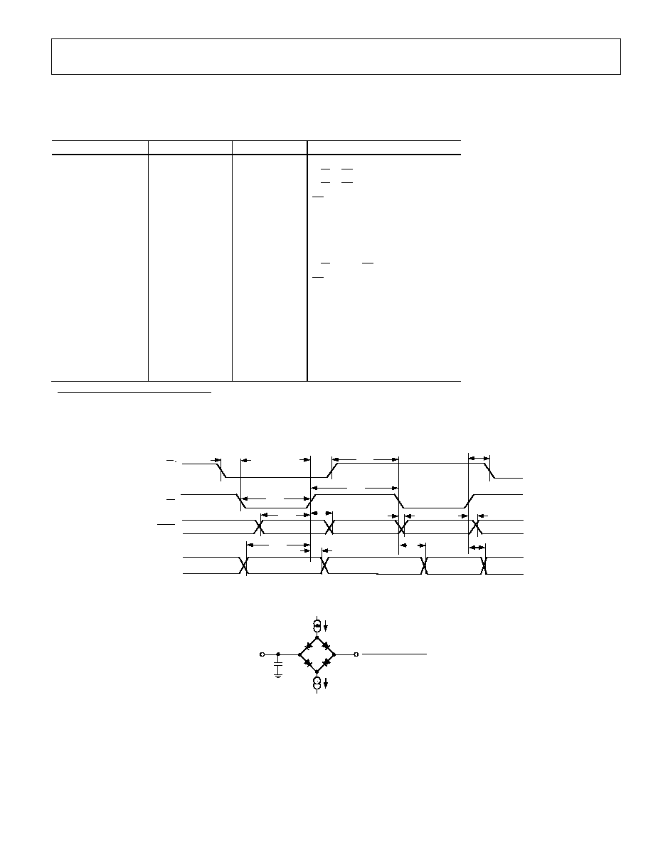
TIMING CHARACTERISTICS
V
DD
= 2.5 V to 5.5 V, V
REF
= 5 V, I
OUT
2 = 0 V. All specifications T
MIN
to T
MAX,
unless otherwise noted.
Table 2.
Parameter
1, 2
Limit at T
MIN
, T
MAX
Unit Conditions/Comments
Write Mode
t
1
0 ns
min
R/W to CS setup time
t
2
0 ns
min
R/W to CS hold time
t
3
10 ns
min
CS low time
t
4
10
ns min
Address setup time
t
5
0
ns min
Address hold time
t
6
6
ns min
Data setup time
t
7
0
ns min
Data hold time
t
8
5 ns
min
R/W high to CS low
t
9
7 ns
min
CS min high time
Data Readback Mode
t
10
0
ns typ
Address setup time
t
11
0
ns typ
Address hold time
t
12
5
ns typ
Data access time
35
ns
max
t
13
5
ns typ
Bus relinquish time
10
ns
max
1
See
Temperature range for Y version is -40°C to +125°C. Guaranteed by design and characterization, not subject to production test.
Figure 2.
2
All input signals are specified with tr = tf = 5ns (10% to 90% of VDD) and timed from a voltage level of (V
IL
+ V
IH
)/2. Digital output timing measured
with load circuit in
.
Figure 3
t
7
DATA VALID
t
6
t
2
CS
R/W
DATA
t
1
DATA VALID
t
2
t
13
t
12
t
3
t
8
t
9
DACA/DACB
t
4
t
5
t
11
t
10
04463-0-002
Figure 2. Timing Diagram
I
OL
200
µ
A
I
OH
200
µ
A
C
L
50pF
TO
OUTPUT
PIN
V
OH (MIN)
+ V
OL (MAX)
2
04463-0-003
Figure 3. Load Circuit for Data Timing Specifications
Document Outline
- FEATURES
- APPLICATIONS
- GENERAL DESCRIPTION
- FUNCTIONAL BLOCK DIAGRAM
- þÿ
- þÿ
- þÿ
- þÿ
- þÿ
- þÿ
- þÿ
- þÿ
- þÿ
- þÿ
- þÿ
- þÿ
- þÿ
- þÿ
- þÿ
- þÿ
- þÿ
- þÿ
- þÿ
- POWER SUPPLIES FOR THE EVALUATION BOARD
- þÿ
- þÿ