
AD5450/AD5451/AD5452/AD5453*
a
REV. PrD Oct, 2003
Information furnished by Analog Devices is believed to be accurate and
reliable. However, no responsibility is assumed by Analog Devices for its
use, nor for any infringements of patents or other rights of third parties
which may result from its use. No license is granted by implication or
otherwise under any patent or patent rights of Analog Devices.
One Technology Way, P.O. Box 9106, Norwood, MA 02062-9106, U.S.A.
Tel: 781/329-4700
World Wide Web Site: http://www.analog.com
Fax: 781/326-8703
Analog Devices, Inc., 2003
8/10/12/14-Bit High Bandwidth
Multiplying DACs with Serial Interface
Preliminary Technical Data
PRELIMINARY TECHNICAL DATA
*US Patent Number 5,689,257
SPI and QSPI are trademarks of Motorola, Inc.
MICROWIRE is a trademark of National Semiconductor Corporation.
FEATURES
+2.5 V to +5.5 V Supply Operation
50MHz Serial Interface
10MHz Multiplying Bandwidth
±10V Reference Input
8-Lead TSOT & MSOP Packages
Pin Compatible 8, 10, 12 and 14 Bit Current Output DACs
Extended Temperature range ≠40∞C to +125∞C
Guaranteed Monotonic
Four Quadrant Multiplication
Power On Reset with brown out detect
<5
µµ
µµ
µ
A typical Current Consumption
APPLICATIONS
Portable Battery Powered Applications
Waveform Generators
Analog Processing
Instrumentation Applications
Programmable Amplifiers and Attenuators
Digitally-Controlled Calibration
Programmable Filters and Oscillators
Composite Video
Ultrasound
Gain, offset and Voltage Trimming
GENERAL DESCRIPTION
The AD5450/AD5451/AD5452/AD5453 are CMOS 8,
10, 12 and 14-bit Current Output digital-to-analog
converters respectively.
These devices operate from a +2.5 V to 5.5 V power sup-
ply, making them suited to battery powered applications
and many other applications.
These DACs utilize double buffered 3-wire serial interface
that is compatible with SPI
TM
, QSPI
TM
, MICROWIRE
TM
and most DSP interface standards.
On power-up, the internal shift register and latches are
filled with zeros and the DAC output is at zero scale.
As a result of manufacture on a CMOS sub micron
process, they offer excellent four quadrant multiplication
characteristics, with large signal multiplying bandwidths
of 10MHz.
FUNCTIONAL BLOCK DIAGRAM
The applied external reference input voltage (V
REF
)
determines the full scale output current. An integrated
feedback resistor (R
FB
) provides temperature tracking and
full scale voltage output when combined with an external
Current to Voltage precision amplifier.
The AD5450/AD5451/AD5452/AD5453 DACs are
available in small 8-lead TSOT & MSOP packages.
CONTROL LOGIC &
INPUT SHIFT REGISTER
SCLK
SYNC
AD5450/
AD5451/
AD5452/
AD5453
V
REF
IOUT1
R
FB
R
8/10/12/14
BIT
R-2R DAC
DAC REGISTER
SDIN
INPUT LATCH
V
DD
Power On
Reset
GND

≠2≠
REV. PrD
AD5450/AD5451/AD5452/AD5453≠SPECIFICATIONS
1
PRELIMINARY TECHNICAL DATA
Parameter
Min
Typ
M a x
Units
Conditions
STATIC PERFORMANCE
A D 5 4 5 0
Resolution
8
Bits
Relative Accuracy
± 0 . 2 5
L S B
Differential Nonlinearity
± Ω
L S B
Guaranteed Monotonic
A D 5 4 5 1
Resolution
1 0
Bits
Relative Accuracy
± 0 . 2 5
L S B
Differential Nonlinearity
± Ω
L S B
Guaranteed Monotonic
A D 5 4 5 2
Resolution
1 2
Bits
Relative Accuracy
± 0 . 5
L S B
Differential Nonlinearity
± Ω
L S B
Guaranteed Monotonic
A D 5 4 5 3
Resolution
1 4
Bits
Relative Accuracy
± 2
L S B
Differential Nonlinearity
± 1
L S B
Guaranteed Monotonic
Total Unadjusted Error
± 2 . 4 4
m V
Gain Error
± 1 . 2 2
m V
Gain Error Temp Coefficient
2
± 5
ppm FSR/∞C
Output Leakage Current
± 1 0
n A
Data = 0000
H
, T
A
= 25∞C, I
OUT1
± 5 0
n A
Data = 0000
H
, I
OUT1
Output Voltage Compliance Range
1 . 2 3
V
REFERENCE INPUT
2
Reference Input Range
± 1 0
V
V
REF
Input Resistance
8
9 . 3
1 2
k
Input resistance TC = -50ppm/∞C
DIGITAL INPUTS
2
Input High Voltage, V
IH
2 . 0
V
V
DD
= 3.6 V to 5 V
1 . 7
V
V
DD
= 2.5 V to 3.6 V
Input Low Voltage, V
IL
0 . 8
V
V
DD
= 2.7 V to 5.5 V
0 . 7
V
V
DD
= 2.5 V to 2.7 V
Input Leakage Current, I
IL
1
µ
A
Input Capacitance
1 0
p F
DYNAMIC PERFORMANCE
2
Reference Multiplying BW
10
MHz
V
REF
= +/-3.5V, DAC loaded all 1s
Output Voltage Settling Time
V
REF
= 10V, R
LOAD
= 100
, C
LOAD
= 15pF
DAC latch alternately loaded with 0s and 1s.
AD5450
1 0 0
n s
Measured to +/-16mV of FS
AD5451
1 1 0
n s
Measured to +/-4mV of FS
AD5452
1 6 0
n s
Measured to +/-1mV of FS
AD5453
1 8 0
n s
Measured to +/-1mV of FS
Digital Delay
2 0
4 0
n s
Interface delay time
10% to 90% Dettling Time
1 0
3 0
n s
Rise and Fall time, V
REF
= 10V, R
LOAD
=
100
,
C
LOAD
= 15pF
Digital to Analog Glitch Impulse
3
nV-s
1 LSB change around Major Carry, V
REF
=0V
Multiplying Feedthrough Error
DAC latch loaded with all 0s.
- 7 5
d B
Reference = 1MHz.
Reference = 10MHz.
Output Capacitance
IOUT1
5
p F
DAC Latches Loaded with all 0s
1 0
p F
DAC Latches Loaded with all 1s
IOUT2
1 0
p F
DAC Latches Loaded with all 0s
5
p F
DAC Latches Loaded with all 1s
Digital Feedthrough
0 . 1
nV-s
Feedthrough to DAC output with
CS high
and Alternate Loading of all 0s and all 1s.
(V
DD
= 2.5 V to 5.5 V, V
REF
= +10 V, I
OUT
x = O V. All specifications T
MIN
to T
MAX
unless otherwise noted. DC performance measured with
OP1177, AC performance with AD9631 unless otherwise noted.)
≠3≠
REV. PrD
AD5450/AD5451/AD5452/AD5453
PRELIMINARY TECHNICAL DATA
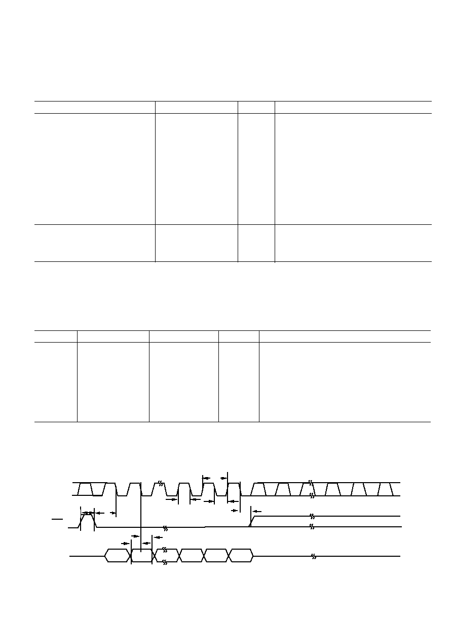
TIMING CHARACTERISTICS
1
Parameter
V
DD
= 4.5 V to 5.5 V
V
DD
= 2.5 V to 5.5 V Units
Conditions/Comments
f
SCLK
50
MHz max
Max Clock frequency
t
1
20
ns min
SCLK Cycle time
t
2
8
ns min
SCLK High Time
t
3
8
ns min
SCLK Low Time
t
4
8
ns min
SYNC falling edge to SCLK active edge setup time
t
5
5
ns min
Data Setup Time
t
6
4.5
ns min
Data Hold Time
t
7
5
ns min
SYNC rising edge to SCLK active edge
t
8
30
ns min
Minimum
SYNC high time
N O T E S
1
See Figures 1.
Temperature range is as follows: Y Version: ≠40∞C to +125∞C.
Guaranteed by design and characterisation, not subject to
production test.
All input signals are specified with tr =tf = 5ns (10% to 90% of V
DD
) and timed from a voltage level of (V
IL
+ V
IH
)/2.
Specifications subject to change without notice.
(V
REF
= +5 V, I
OUT
2 = O V. All specifications T
MIN
to T
MAX
unless otherwise noted.)
t1
DB15
DB0
t2
t3
t4
t5
t6
t8
SCLK
SYNC
DIN
t7
Parameter
Min
Typ
M a x
Units
Conditions
Total Harmonic Distortion
- 8 0
d B
V
REF
= 3.5 V pk-pk, All 1s loaded, f = 1kHz
Digital THD, Clock = 1MHz
50kHz f
OUT
7 5
d B
Output Noise Spectral Density
2 5
nV/
H z
@ 1kHz
SFDR performance (Wideband)
Update = 1MHz, V
REF
= 3.5V
Update = 1MHz
50kHz Fout
7 8
d B
20kHz Fout
7 8
d B
SFDR performance (NarrowBand)
Update = 1MHz, V
REF
= 3.5V
50kHz Fout
8 7
d B
20kHz Fout
8 7
d B
Intermodulation Distortion
7 8
d B
f1 = 20kHz, f2 = 25kHz, Update=1MHz,
V
REF
=3.5V
POWER REQUIREMENTS
Power Supply Range
2 . 5
5 . 5
V
I
DD
1
µ
A
Logic Inputs = 0 V or V
DD
Power Supply Sensitivity
2
0.001
% / %
V
DD
= ±5%
N O T E S
1
Temperature range is as follows: Y Version: ≠40∞C to +125∞C.
2
Guaranteed by design and characterisation, not subject to production test.
Specifications subject to change without notice.
Figure 1. Timing Diagram.
(V
DD
= 2.5 V to 5.5 V, V
REF
= +10 V, I
OUT
x = O V. All specifications T
MIN
to T
MAX
unless otherwise noted. DC performance measured with
OP1177, AC performance with AD9631 unless otherwise noted.)

≠4≠
REV. PrD
AD5450/AD5451/AD5452/AD5453
PRELIMINARY TECHNICAL DATA
ABSOLUTE MAXIMUM RATINGS
1, 2
(T
A
= +25∞C unless otherwise noted)
V
DD
to GND
≠0.3 V to +7 V
V
REF,
R
FB
to GND
≠12 V to +12 V
I
OUT
1 to GND
≠0.3 V to +7 V
Input Current to any pin except supplies
±10 mA
Logic Inputs & Output
3
-0.3V to V
DD
+0.3 V
Operating Temperature Range
Industrial (Y Version)
≠40∞C to +125∞C
Storage Temperature Range
≠65∞C to +150∞C
Junction Temperature
+150∞C
8 lead MSOP
JA
Thermal Impedance
206∞C/W
8 lead TSOT
JA
Thermal Impedance
211∞C/W
Lead Temperature, Soldering (10seconds)
300∞C
IR Reflow, Peak Temperature (<20 seconds)
+235∞C
NOTES
1
Stresses above those listed under "Absolute Maximum Ratings" may cause permanent
damage to the device. This is a stress rating only and functional operation of the device
at these or any other conditions above those listed in the operational sections of this
specification is not implied. Exposure to absolute maximum rating conditions for
extended periods may affect device reliability. Only one absolute maximum rating may
be applied at any one time.
2
Transient currents of up to 100mA will not cause SCR latchup.
3
Overvoltages at SCLK,
SYNC, DIN, will be clamped by internal diodes. Current
should be limited to the maximum ratings given.
CAUTION
ESD (electrostatic discharge) sensitive device. Electrostatic charges as high as 4000 V readily
accumulate on the human body and test equipment and can discharge without detection.
Although the AD5450/AD5451/AD5452/AD5453 features proprietary ESD protection circuitry,
permanent damage may occur on devices subjected to high energy electrostatic discharges. Therefore,
proper ESD precautions are recommended to avoid performance degradation or loss of functionality.
ORDERING GUIDE
Model
Resolution
INL
Temperature Range
Package Description Branding
Package Option
AD5450YUJ
8
±0.25
-40
o
C to +125
o
C
T S O T
UJ-8
AD5451YUJ
10
±0.25
-40
o
C to +125
o
C
T S O T
UJ-8
AD5452YUJ
12
±0.5
-40
o
C to +125
o
C
T S O T
UJ-8
AD5452YRM 12
±0.5
-40
o
C to +125
o
C
M S O P
RM-8
AD5453YUJ
14
±2
-40
o
C to +125
o
C
T S O T
UJ-8
AD5453YRM 14
±2
-40
o
C to +125
o
C
M S O P
RM-8
AD5450/AD5451/AD5452/AD5453
≠5≠
REV. PrD
PRELIMINARY TECHNICAL DATA
PIN FUNCTION DESCRIPTION
MSOP
TSOT
Mnemonic Function
1
8
I
OUT
1
DAC Current Output.
2
7
G N D
Ground Pin.
3
6
SCLK
Serial Clock Input. By default, data is clocked into the input shift register on the
falling edge of the serial clock input. Alternatively, by means of the serial control
bits, the device may be configured such that data is clocked into the shift register on
the rising edge of SCLK.
4
5
S D I N
Serial Data Input. Data is clocked into the 16-bit input register on the active edge of
the serial clock input. By default, on power up, data is clocked into the shift register
on the falling edge of SCLK. The control bits allow the user to change the active
edge to rising edge.
5
4
S Y N C
Active Low Control Input. This is the frame synchronization signal for the input
data. Data is loaded to the shift register on the active edge of the
following clocks.
6
3
V
D D
Positive power supply input. These parts can operate from a supply of +2.5 V to
+5.5 V.
7
2
V
REF
DAC reference voltage input pin.
8
1
R
F B
DAC feedback resistor pin. Establish voltage output for the DAC by connecting to
external amplifier output.
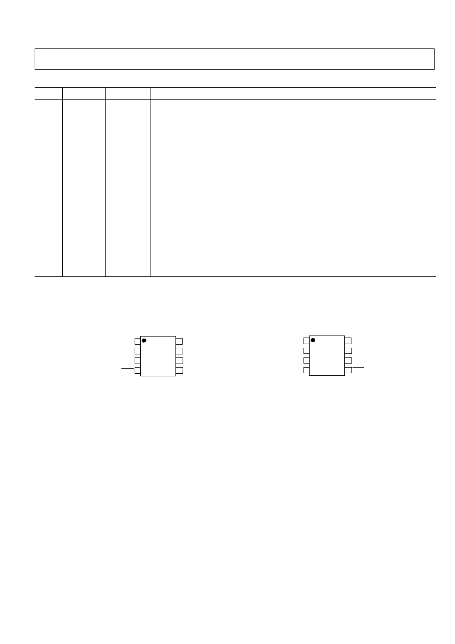
PIN CONFIGURATION
AD5452/
AD5453
(Not to Scale)
IOUT1
GND
SCLK
SDIN
1
2
3
4
5
6
7
8 RFB
VREF
VDD
SYNC
AD5450/
AD5451/
AD5452/
AD5453
(Not to Scale)
IOUT1
GND
SCLK
SDIN
1
2
3
4
5
6
7
8
RFB
VREF
VDD
SYNC
MSOP (RM-8)
TSOT (UJ-8)