 | ÐлекÑÑоннÑй компоненÑ: AD546K | СкаÑаÑÑ:  PDF PDF  ZIP ZIP |
Äîêóìåíòàöèÿ è îïèñàíèÿ www.docs.chipfind.ru
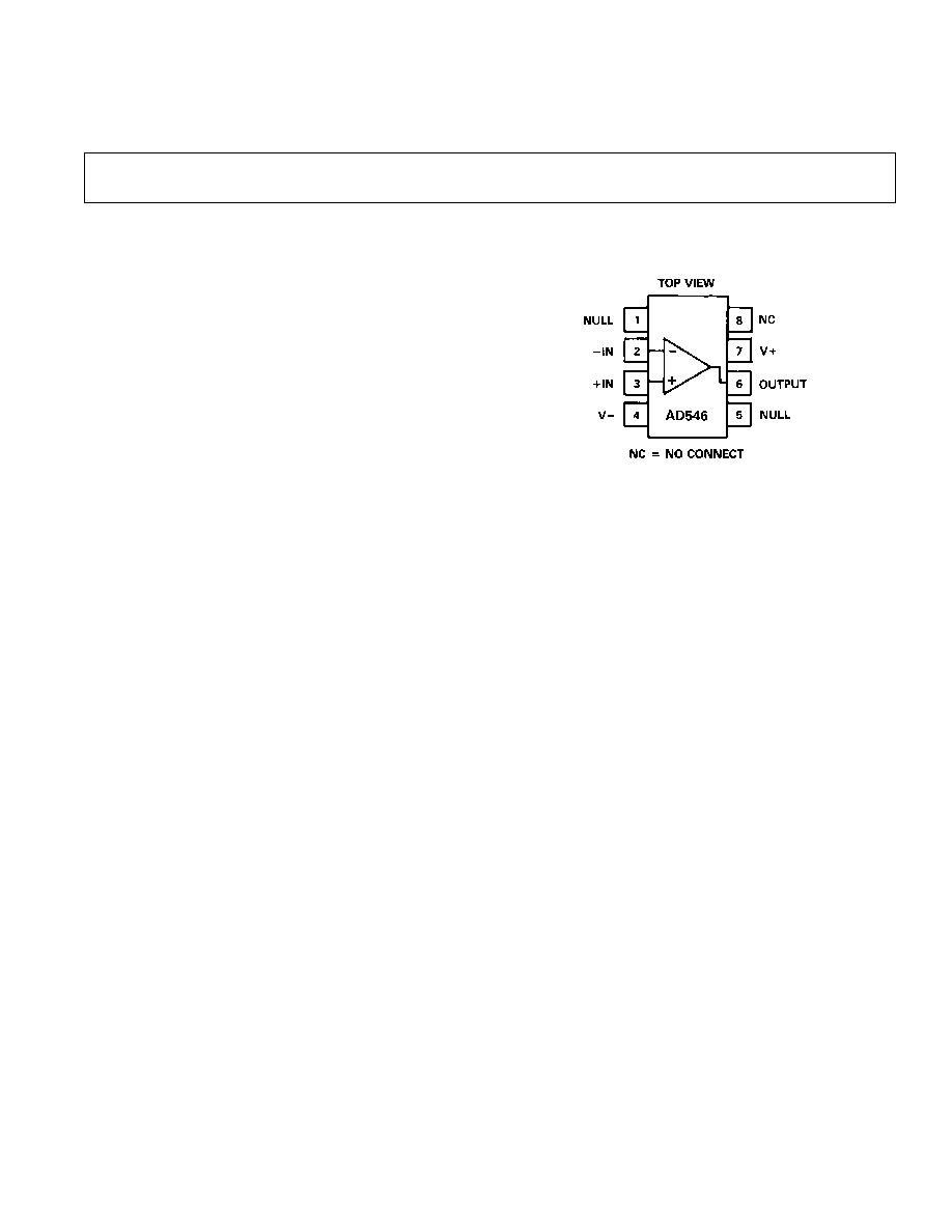
CONNECTION DIAGRAM
8-Pin Plastic
Mini-DIP Package
REV. A
Information furnished by Analog Devices is believed to be accurate and
reliable. However, no responsibility is assumed by Analog Devices for its
use, nor for any infringements of patents or other rights of third parties
which may result from its use. No license is granted by implication or
otherwise under any patent or patent rights of Analog Devices.
a
1 pA Monolithic Electrometer
Operational Amplifier
AD546*
One Technology Way, P.O. Box 9106, Norwood, MA 02062-9106, U.S.A.
Tel: 617/329-4700
Fax: 617/326-8703
FEATURES
DC PERFORMANCE
1 mV max Input Offset Voltage
Low Offset Drift: 20 V/ C
1 pA max Input Bias Current
Input Bias Current Guaranteed Over Full
Common-Mode Voltage Range
AC PERFORMANCE
3 V/ s Slew Rate
1 MHz Unity Gain Bandwidth
Low Input Voltage Noise: 4 V p-p, 0.1 Hz to 10 Hz
Available in a Low Cost, 8-Pin Plastic Mini-DIP
Standard Op Amp Pinout
APPLICATIONS
Electrometer Amplifiers
Photodiode Preamps
pH Electrode Buffers
Log Ratio Amplifiers
PRODUCT DESCRIPTION
The AD546 is a monolithic electrometer combining the virtues
of low (1 pA) input bias current with the cost effectiveness of a
plastic mini-DIP package. Both input offset voltage and input
offset voltage drift are laser trimmed, providing very high perfor-
mance for such a low cost amplifier.
Input bias currents are reduced significantly by using "topgate"
JFET technology. The 10
15
common-mode impedance,
resulting from a bootstrapped input stage, insures that input
bias current is essentially independent of common-mode voltage
variations.
The AD546 is suitable for applications requiring both minimal
levels of input bias current and low input offset voltage. Appli-
cations for the AD546 include use as a buffer amplifier for cur-
rent output transducers such as photodiodes and pH probes. It
may also be used as a precision integrator or as a low droop rate
sample and hold amplifier. The AD546 is pin compatible with
standard op amps; its plastic mini-DIP package is ideal for use
with automatic insertion equipment.
The AD546 is available in two performance grades, all rated
over the 0
°
C to +70
°
C commercial temperature range, and
packaged in an 8-pin plastic mini-DIP.
*Covered by Patent No. 4,639,683.
PRODUCT HIGHLIGHTS
1. The input bias current of the AD546 is specified, 100%
tested and guaranteed with the device in the fully warmed-up
condition.
2. The input offset voltage of the AD546 is laser trimmed to
less than 1 mV (AD546K).
3. The AD546 is packaged in a standard, low cost, 8-pin
mini-DIP.
4. A low quiescent supply current of 700
µ
A minimizes any
thermal effects which might degrade input bias current and
input offset voltage specifications.

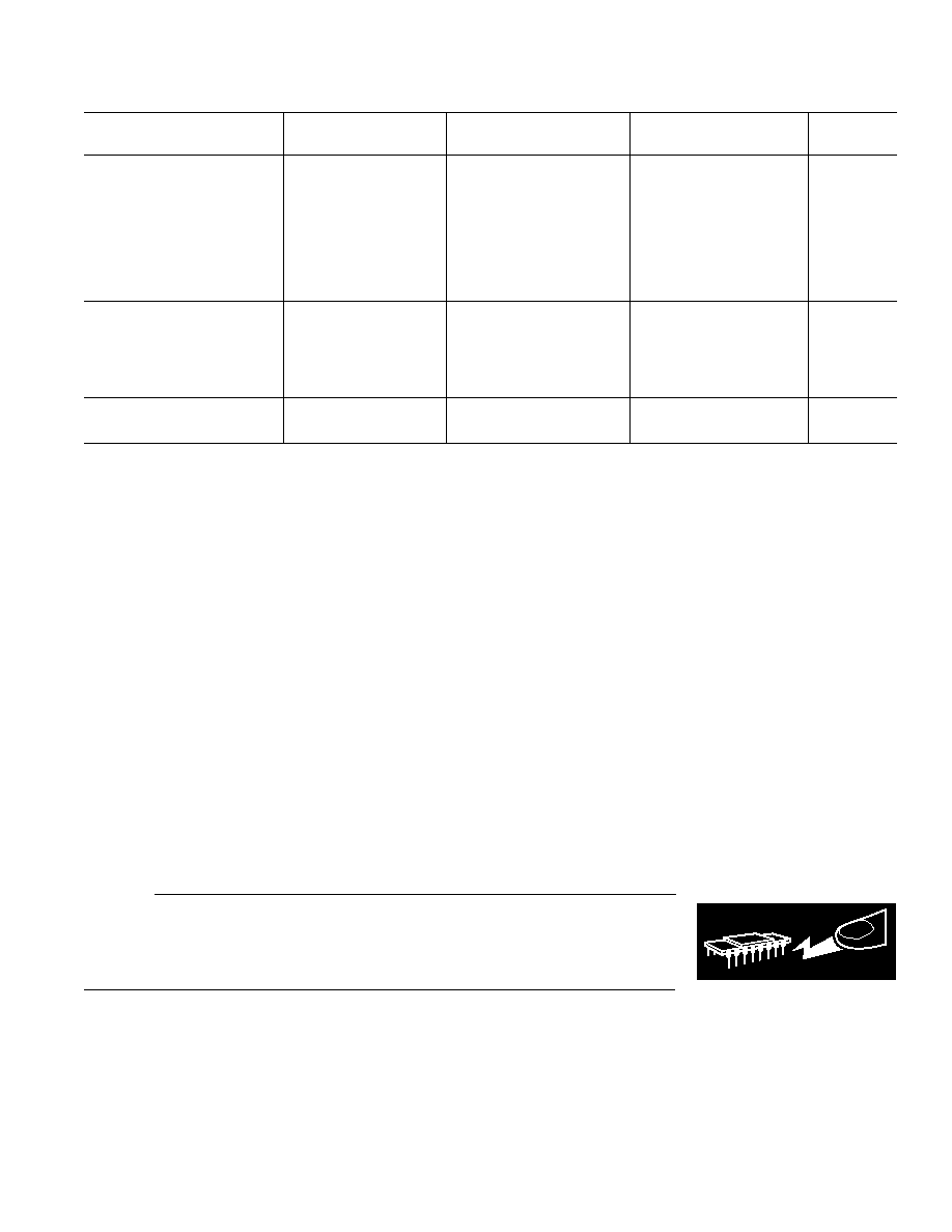
AD546SPECIFICATIONS
(@ +25 C and 15 V dc, unless otherwise noted)
REV. A
2
AD546J
AD546K
Model
Conditions
Min
Typ
Max
Min
Typ
Max
Units
INPUT BIAS CURRENT
1
Either Input
V
CM
= 0 V
0.2
1
0.2
0.5
pA
Either Input
V
CM
=
±
10 V
0.1
1
0.2
0.5
pA
Either Input
@ T
MAX
V
CM
= 0 V
40
20
pA
Either Input
V
CM
=
±
10 V
40
20
pA
Offset Current
V
CM
= 0 V
0.17
0.09
pA
Offset Current
@ T
MAX
V
CM
= 0 V
13
7
pA
INPUT OFFSET
Initial Offset
2
1
pA
Offset @ T
MAX
3
2
mV
vs. Temperature
20
20
µ
V/
°
C
vs. Supply
100
100
µ
V/V
vs. Supply
T
MIN
T
MAX
100
100
µ
V/V
Long-Term Stability
20
20
µ
V/Month
INPUT VOLTAGE NOISE
f = 0.1 Hz to 10 Hz
4
4
µ
V p-p
f = 10 Hz
90
90
nV/
Hz
f = 100 Hz
60
60
nV/
Hz
f
= 1 kHz
35
35
nV/
Hz
f = 10 kHz
35
35
nV/
Hz
INPUT CURRENT NOISE
f = 0.1 Hz to 10 Hz
1.3
1.3
fA rms
f = 1 kHz
0.4
0.4
fA/
Hz
INPUT IMPEDANCE
Differential
V
DIFF
=
±
1 V
10
13
1
10
13
1
pF
Common Mode
V
CM
=
±
10 V
10
15
0.8
10
15
0.8
pF
OPEN LOOP GAIN
V
O
=
±
10 V
R
LOAD
= 10 k
300
1000
300
1000
V/mV
T
MIN
T
MAX
V
O
=
±
10 V
R
LOAD
= 10 k
300
800
300
800
V/mV
V
O
=
±
10 V
R
LOAD
= 2 k
100
250
100
250
V/mV
T
MIN
T
MAX
V
O
=
±
10 V
R
LOAD
= 2 k
80
200
80
200
V/mV
INPUT VOLTAGE RANGE
Differential
3
±
20
±
20
V
Common-Mode Voltage
10
+10
10
+10
V
Common-Mode Rejection Ratio
V
CM
=
±
10 V
80
90
84
100
dB
T
MIN
to T
MAX
76
80
76
80
dB
OUTPUT CHARACTERISTICS
Voltage
R
LOAD
= 10 k
12
+12
12
+12
V
R
LOAD
= 2 k
10
+10
10
+10
V
Current
Short Circuit
15
20
35
15
20
35
mA
Load Capacitance Stability
Gain = +1
4000
4000
pF
AD546
AD546J
AD546K
Model
Conditions
Min
Typ
Max
Min
Typ
Max
Units
FREQUENCY RESPONSE
Gain BW, Small Signal
G = 1
0.7
1.0
0.7
1.0
MHz
Full Power Response
V
O
= 20 V p-p
50
50
kHz
Slew Rate, Unity Gain
G = 1
2
3
2
3
V/
µ
s
Settling Time
to 0.1%
4.5
4.5
µ
s
to 0.01%
5
5
µ
s
Overload Recovery
50% Overdrive
Gain = 1
2
2
µ
s
POWER SUPPLY
Rated Performance
±
15
±
15
V
Operating Range
5
18
5
18
V
Quiescent Current
0.60
0.7
0.60
0.7
mA
Transistor Count
# of Transistors
50
50
PACKAGE OPTIONS
Plastic Mini-DIP (N-8)
AD546JN
AD546KN
NOTES
1
Bias current specifications are guaranteed maximum, at either input, after 5 minutes of operation at T
A
= +25
°
C. Bias current increases by a factor of 2.3 for
every 10
°
C rise in temperature.
2
Input offset voltage specifications are guaranteed after 5 minutes of operation at T
A
= +25
°
C.
3
Defined as max continuous voltage between inputs, such that neither exceeds
±
10 V from ground.
Specifications subject to change without notice.
Specifications in boldface are tested on all production units at final electrical test. Results from those tests are used to calculate outgoing quality levels. All min and
max specifications are guaranteed, although only those shown in boldface are tested on all production units.
3
REV. A
ABSOLUTE MAXIMUM RATINGS
1
Supply Voltage . . . . . . . . . . . . . . . . . . . . . . . . . . . . . . . .
±
18 V
Internal Power Dissipation . . . . . . . . . . . . . . . . . . . . . . 500 mW
Input Voltage
2
. . . . . . . . . . . . . . . . . . . . . . . . . . . . . . . .
±
18 V
Output Short Circuit Duration . . . . . . . . . . . . . . . . . Indefinite
Differential Input Voltage . . . . . . . . . . . . . . . . . . +V
S
and V
S
Storage Temperature Range . . . . . . . . . . . . . 65
°
C to +125
°
C
Operating Temperature Range . . . . . . . . . . . . . . 0
°
C to +70
°
C
Lead Temperature Range (Soldering 60 sec) . . . . . . . . +300
°
C
NOTES
1
Stresses above those listed under "Absolute Maximum Ratings" may cause
permanent damage to the device. This is a stress rating only and functional
operation of the device at these or any other conditions above those indicated in the
operational section of this specification is not implied. Exposure to absolute
maximum rating conditions for extended periods may affect device reliability.
2
For supply voltages less than
±
18 V, the absolute maximum input voltage is equal
to the supply voltage.
WARNING!
ESD SENSITIVE DEVICE
CAUTION
ESD (electrostatic discharge) sensitive device. Electrostatic charges as high as 4000 V readily
accumulate on the human body and test equipment and can discharge without detection.
Although the AD546 features proprietary ESD protection circuitry, permanent damage may
occur on devices subjected to high energy electrostatic discharges. Therefore, proper ESD
precautions are recommended to avoid performance degradation or loss of functionality.
AD546Typical Characteristics
(V
S
= 15 V, unless otherwise noted)
SUPPLY VOLTAGE
±
V
INPUT VOLTAGE RANGE
±
V
20
15
0
0
5
20
10
15
10
5
+V
IN
V
IN
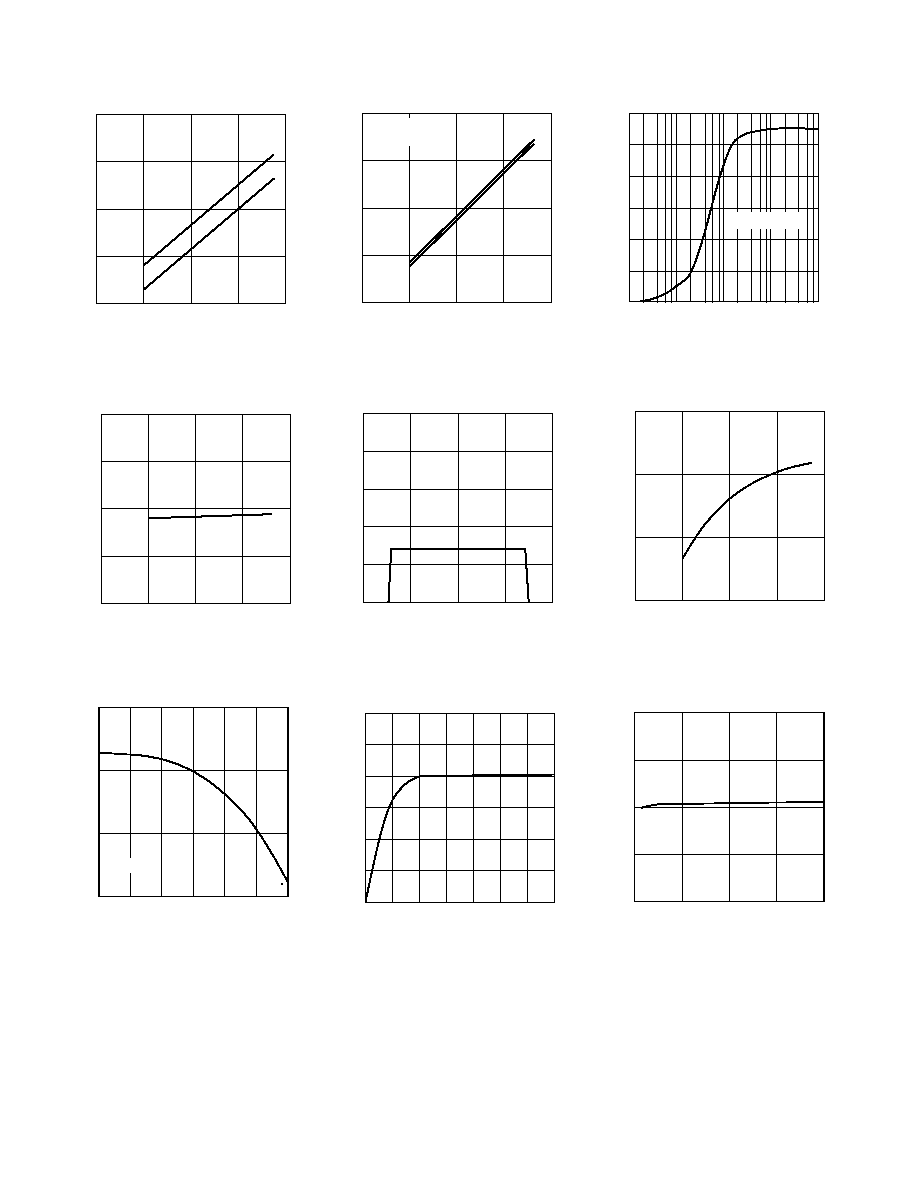
Figure 1. Input Voltage Range
vs. Supply Voltage
SUPPLY VOLTAGE
±
V
800
700
400
0
5
20
10
15
600
500
QUIESCENT CURRENT µA
Figure 4. Quiescent Current vs.
Supply Voltage
OPEN LOOP GAIN V/mV
TEMPERATURE
o
C
3000
1000
100
55
25
125
5
35
65
95
300
R
L
= 10k
Figure 7. Open Loop Gain vs.
Temperature
SUPPLY VOLTAGE
±
V
20
15
0
0
5
20
10
15
10
5
OUTPUT VOLTAGE RANGE
±
V
+25
o
C
R
L
= 10k
+V
OUT
V
OUT
Figure 2. Output Voltage Range
vs. Supply Voltage
INPUT COMMON MODE VOLTAGE V
120
COMMON MODE REJECTION RATIO dB
110
70
15
+15
10
0
+10
100
90
80
Figure 5. CMRR vs. Input
Common-Mode Voltage
WARM-UP TIME Minutes
30
0
0
1
7
2
3
4
5
6
25
20
15
10
5
|VOS| µV
Figure 8. Change in Offset
Voltage vs. Warm-Up Time
30
15
0
100k
10k
1k
10
10
5
20
25
LOAD RESISTANCE
OUTPUT VOLTAGE SWING Volts p-p
100
V
S
=
±
15 VOLTS
Figure 3. Output Voltage Swing
vs. Resistive Load
R
L
= 10k
SUPPLY VOLTAGE
±
V
OPEN LOOP GAIN V/mV
3000
1000
100
0
5
20
10
15
300
Figure 6. Open Loop Gain vs.
Supply Voltage
COMMON-MODE VOLTAGE Volts
300
250
100
10
5
10
0
5
200
150
+25
o
C
INPUT BIAS CURRENT fA
Figure 9. Input Bias Current vs.
Common-Mode Voltage
REV. A
4
AD546
REV. A
5
SUPPLY VOLTAGE
±
VOLTS
300
250
100
0
5
20
10
15
200
150
INPUT BIAS CURRENT fA
+25
o
C
Figure 10. Input Bias Current
vs. Supply Voltage
FREQUENCY Hz
OPEN LOOP GAIN dB
100
40
10
100
10M
1k
10k
100k
1M
80
60
40
0
20
20
PHASE MARGIN Degrees
100
40
80
60
40
0
20
20
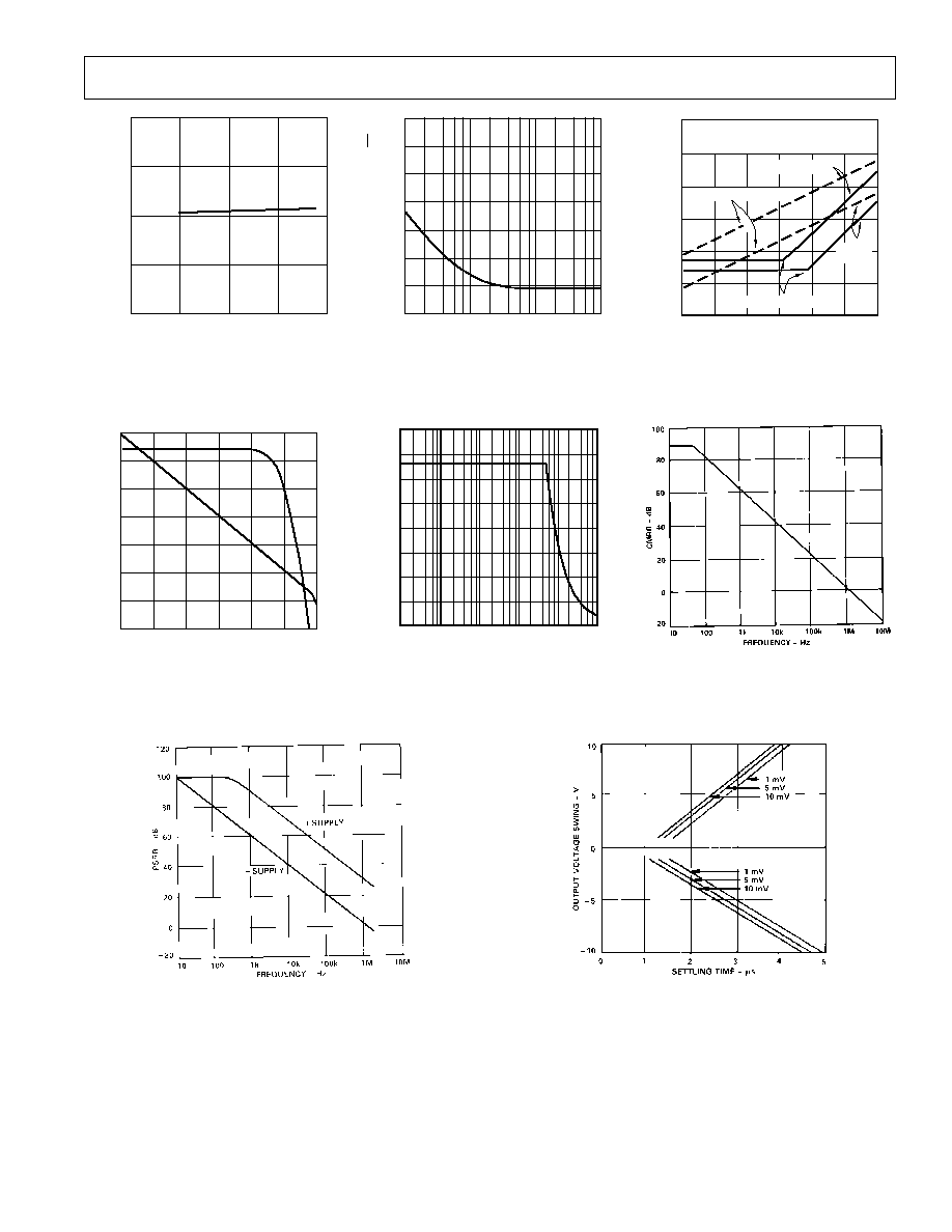
Figure 13. Open Loop Frequency
Response
160
100
20
10k
1k
10
60
40
120
140
FREQUENCY Hz
100
80
NOISE SPECTRAL DENSITY nV/
Hz
Figure 11. Input Voltage Noise
Spectral Density vs. Frequency
40
0
1M
20
5
100
15
10
35
30
100k
10k
1k
FREQUENCY Hz
10
25
OUTPUT VOLTAGE SWING V
Figure 14. Large Signal Frequency
Response
SOURCE RESISTANCE Ohms
100k
0.1
100k
1M
100G
10M
100M
1G
10G
10k
1k
100
10
INPUT NOISE VOLTAGE µV p-p
1
WHENEVER JOHNSON NOISE IS GREATER THAN
AMPLIFIER NOISE, AMPLIFIER NOISE CAN BE
CONSIDERED NEGLIGIBLE FOR THE APPLICATION.
RESISTOR JOHNSON NOISE
1 kHz BANDWIDTH
AMPLIFIER GENERATED NOISE
10 Hz
BANDWIDTH
Figure 12. Noise vs. Source
Resistance
Figure 15. CMRR vs. Frequency
Figure 16. PSRR vs. Frequency
Figure 17. Output Settling Time vs.
Output Swing and Error Voltage