 | ÐлекÑÑоннÑй компоненÑ: AD548BR | СкаÑаÑÑ:  PDF PDF  ZIP ZIP |
Äîêóìåíòàöèÿ è îïèñàíèÿ www.docs.chipfind.ru
a
AD548
Precision, Low Power
BiFET Op Amp
REV. B
Information furnished by Analog Devices is believed to be accurate and
reliable. However, no responsibility is assumed by Analog Devices for its
use, nor for any infringements of patents or other rights of third parties
which may result from its use. No license is granted by implication or
otherwise under any patent or patent rights of Analog Devices.
FEATURES
Enhanced Replacement for LF441 and TL061
DC Performance:
200 A max Quiescent Current
10 pA max Bias Current, Warmed Up (AD548C)
250 V max Offset Voltage (AD548C)
2 V/ C max Drift (AD548C)
2 V p-p Noise, 0.1 Hz to 10 Hz
AC Performance:
1.8 V/ s Slew Rate
1 MHz Unity Gain Bandwidth
Available in Plastic, Hermetic Cerdip and Hermetic
Metal Can Packages and in Chip Form
Available in Tape and Reel in Accordance with
EIA-481A Standard
MIL-STD-883B Parts Available
Dual Version Available: AD648
Surface Mount (SOIC) Package Available
PRODUCT DESCRIPTION
The AD548 is a low power, precision monolithic operational
amplifier. It offers both low bias current (10 pA max, warmed
up) and low quiescent current (200
µ
A max) and is fabricated
with ion-implanted FET and laser wafer trimming technologies.
Input bias current is guaranteed over the AD548's entire
common-mode voltage range.
The economical J grade has a maximum guaranteed input offset
voltage of less than 2 mV and an input offset voltage drift of less
than 20
µ
V/
°
C. The C grade reduces input offset voltage to less
than 0.25 mV and offset voltage drift to less than 2
µ
V/
°
C. This
level of dc precision is achieved utilizing Analog's laser wafer
drift trimming process. The combination of low quiescent cur-
rent and low offset voltage drift minimizes changes in input off-
set voltage due to self-heating effects. Four additional grades are
offered over the commercial, industrial and military temperature
ranges.
The AD548 is recommended for any dual supply op amp appli-
cation requiring low power and excellent dc and ac perfor-
mance. In applications such as battery-powered, precision
instrument front ends and CMOS DAC buffers, the AD548's
excellent combination of low input offset voltage and drift, low
bias current and low 1/f noise reduces output errors. High com-
mon-mode rejection (86 dB, min on the "C" grade) and high
open-loop gain ensures better than 12-bit linearity in high im-
pedance, buffer applications.
The AD548 is pinned out in a standard op amp configuration
and is available in six performance grades. The AD548J and
AD548K are rated over the commercial temperature range of
0
°
C to +70
°
C. The AD548A, AD548B and AD548C are rated
over the industrial temperature range of 40
°
C to +85
°
C. The
AD548S is rated over the military temperature range of 55
°
C
to +125
°
C and is available processed to MIL-STD-883B, Rev. C.
The AD548 is available in an 8-pin plastic mini-DIP, cerdip,
TO-99 metal can, surface mount (SOIC), or in chip form.
PRODUCT HIGHLIGHTS
1. A combination of low supply current, excellent dc and ac
performance and low drift makes the AD548 the ideal op
amp for high performance, low power applications.
2. The AD548 is pin compatible with industry standard op
amps such as the LF441, TL061, and AD542, enabling de-
signers to improve performance while achieving a reduction
in power dissipation of up to 85%.
3. Guaranteed low input offset voltage (2 mV max) and drift
(20
µ
V/
°
C max) for the AD548J are achieved utilizing
Analog Devices' laser drift trimming technology, eliminating
the need for external trimming.
4. Analog Devices specifies each device in the warmed-up con-
dition, insuring that the device will meet its published specifi-
cations in actual use.
5. A dual version, the AD648 is also available.
6. Enhanced replacement for LF441 and TL061.
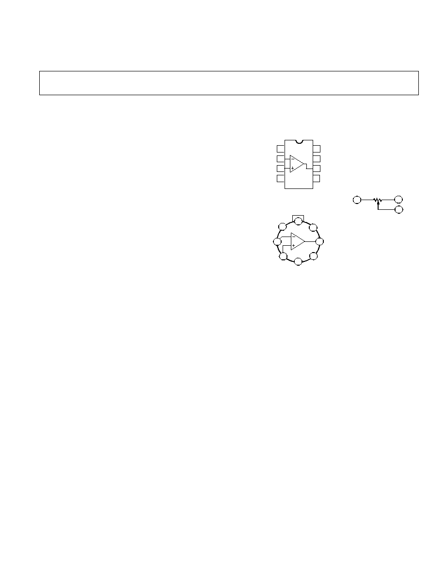
CONNECTION DIAGRAMS
Plastic Mini-DIP (N) Package,
Cerdip (Q) Package and
SOIC (R)Package
AD548
OFFSET NULL
OUTPUT
NC
V
OFFSET
NULL
NONINVERTING
INPUT
6
7
1
3
4
5
2
8
V+
NOTE : PIN 4 CONNECTED TO CASE
NC = NO CONNECT
INVERTING
INPUT
1
2
3
4
8
7
6
5
AD548
OFFSET NULL
V+
OUTPUT
NC
INVERTING
INPUT
V
OFFSET
NULL
TOP VIEW
NONINVERTING
INPUT
1
4
5
V
OS
TRIM
TOP VIEW
15V
10k
One Technology Way, P.O. Box 9106, Norwood, MA 02062-9106, U.S.A.
Tel: 617/329-4700
Fax: 617/326-8703
TO-99 (H) Package

AD548SPECIFICATIONS
Model
AD548J/A/S
AD548K/B
AD548C
Min
Typ
Max
Min
Typ
Max
Min
Typ
Max
Units
INPUT OFFSET VOLTAGE
1
Initial Offset
0.75
2.0
0.3
0.5
0.10
0.25
mV
T
MIN
to T
MAX
3.0/3.0/3.0
0.7/0.8
0.4
mV
vs. Temperature
20
5
2.0
µ
V/
°
C
vs. Supply
80
86
86
dB
vs. Supply, T
MIN
to T
MAX
76/76/76
80
80
dB
Long-Term Offset Stability
15
15
15
µ
V/Month
INPUT BIAS CURRENT
Either Input
2
, V
CM
= 0
5
20
3
10
3
10
pA
Either Input
2
at T
MAX
, V
CM
= 0
0.45/1.3/20
0.25/0.65
0.65
nA
Max Input Bias Current Over
Common-Mode Voltage Range
30
15
15
pA
Offset Current, V
CM
= 0
5
10
2
5
2
5
pA
Offset Current at T
MAX
0.25/0.65/10
0.15/0.35
0.35
nA
INPUT IMPEDANCE
Differential
1
×
10
12
3
1
×
10
12
3
1
×
10
12
3
pF
Common Mode
3
×
10
12
3
3
×
10
12
3
3
×
10
12
3
pF
INPUT VOLTAGE RANGE
Differential
3
±
20
±
20
±
20
V
Common Mode
±
11
±
12
±
11
±
12
±
11
±
12
V
Common-Mode Rejection
V
CM
=
±
10 V
76
90
82
92
86
98
dB
T
MIN
to T
MAX
76/76/76
90
82
92
86
98
dB
V
CM
=
±
11 V
70
84
76
86
76
90
dB
T
MIN
to T
MAX
70/70/70
84
76
86
76
90
dB
INPUT VOLTAGE NOISE
Voltage 0.1 Hz to 10 Hz
2
2
2
4.0
µ
V p-p
f = 10 Hz
80
80
80
nV/
Hz
f = 100 Hz
40
40
40
nV/
Hz
f = 1 kHz
30
30
30
nV/
Hz
f = 10 kHz
30
30
30
nV/
Hz
INPUT CURRENT NOISE
f = 1 kHz
1.8
1.8
1.8
fA/
Hz
FREQUENCY RESPONSE
Unity Gain, Small Signal
0.8
1.0
0.8
1.0
0.8
1.0
MHz
Full Power Response
30
30
30
kHz
Slew Rate, Unity Gain
1.0
1.8
1.0
1.8
1.0
1.8
V/
µ
s
Settling Time to
±
0.01%
8
8
8
µ
s
OPEN LOOP GAIN
V
O
=
±
10 V, R
L
10 k
300
1000
300
1000
300
1000
V/mV
T
MIN
to T
MAX
, R
L
10 k
300/300/300
700
300
700
300
700
V/mV
V
O
=
±
10 V, R
L
5 k
150
500
150
500
150
500
V/mV
T
MIN
to T
MAX
, R
L
5 k
150/150/150
300
150
300
150
300
V/mV
OUTPUT CHARACTERISTICS
Voltage @ R
L
10 k
,
±
12
±
13
±
12
±
13
±
12
±
13
V
T
MIN
to T
MAX
±
12/
±
12/
±
12
±
12
±
12
Voltage @ R
L
5 k
,
±
11
±
12.3
±
11
±
12.3
±
11
±
12.3
V
T
MIN
to T
MAX
±
11/
±
11/
±
11
±
11
±
11
Short Circuit Current
15
15
15
mA
POWER SUPPLY
Rated Performance
±
15
±
15
±
15
V
Operating Range
±
4.5
±
18
±
4.5
±
18
±
4.5
±
18
V
Quiescent Current
170
200
170
200
170
200
µ
A
TEMPERATURE RANGE
Operating, Rated Performance
Commercial (0
°
C to +70
°
C)
AD548J
AD548K
Industrial (40
°
C to +85
°
C)
AD548A
AD548B
AD548C
Military (55
°
C to +125
°
C)
AD548S
PACKAGE OPTIONS
SOIC (R-8)
AD548JR
AD548KR, AD548BR
Plastic (N-8)
AD548JN
AD548KN
Cerdip (Q-8)
AD548AQ
AD548CQ
Metal Can (H-08A)
AD548AH
AD548BH
Tape and Reel
AD548JR-REEL
AD548KR-REEL, AD548BR-REEL
Chips Available
AD548JCHIPS
NOTES
1
Input Offset Voltage specifications are guaranteed after 5 minutes of operation at T
A
= +25
°
C.
2
Bias Current specifications are guaranteed maximum at either input after 5 minutes of operation at T
A
= +25
°
C. For higher temperature, the current doubles every 10
°
C.
3
Defined as voltages between inputs, such that neither exceeds
±
10 V from ground.
Specifications subject to change without notice.
(@ +25 C and V
S
=
15 V dc unless otherwise noted)
REV. C
2
AD548
REV. C
3
WARNING!
ESD SENSITIVE DEVICE
CAUTION
ESD (electrostatic discharge) sensitive device. Electrostatic charges as high as 4000 V readily
accumulate on the human body and test equipment and can discharge without detection.
Although the AD548 features proprietary ESD protection circuitry, permanent damage may
occur on devices subjected to high energy electrostatic discharges. Therefore, proper ESD
precautions are recommended to avoid performance degradation or loss of functionality.
ABSOLUTE MAXIMUM RATINGS
l
Supply Voltage . . . . . . . . . . . . . . . . . . . . . . . . . . . . . . . . .
±
18 V
Internal Power Dissipation
2
. . . . . . . . . . . . . . . . . . . . 500 mW
Input Voltage
3
. . . . . . . . . . . . . . . . . . . . . . . . . . . . . . . . .
±
18 V
Output Short Circuit Duration . . . . . . . . . . . . . . . . . Indefinite
Differential Input Voltage . . . . . . . . . . . . . . . . . . +V
S
and V
S
Storage Temperature Range (Q, H) . . . . . . . . 65
°
C to +150
°
C
(N, R) . . . . . . . . 65
°
C to +125
°
C
Operating Temperature Range
AD548J/K . . . . . . . . . . . . . . . . . . . . . . . . . . . . 0
°
C to +70
°
C
AD548A/B/C . . . . . . . . . . . . . . . . . . . . . . . . 40
°
C to +85
°
C
AD548S . . . . . . . . . . . . . . . . . . . . . . . . . . . 55
°
C to +125
°
C
Lead Temperature Range (Soldering 60 sec) . . . . . . . . +300
°
C
NOTES
1
Stresses above those listed under "Absolute Maximum Ratings" may cause
permanent damage to the device. This is a stress rating only and functional
operation of the device at these or any other conditions above those indicated in the
operational sections of this specification is not implied. Exposure to absolute
maximum rating conditions for extended periods may affect device reliability.
2
Thermal Characteristics: 8-Pin SOIC Package:
JA
= 160
°
C/W,
JC
= 42
°
C/W;
8-Pin Plastic Package:
JA
= 90
°
C/W; 8-Pin Cerdip Package:
JC
= 22
°
C/W,
JA
=
110
°
C/W; 8-Pin Metal Can Package:
JC
= 65
°
C/W,
JA
= 150
°
C/W.
3
For supply voltages less than
±
18 V, the absolute maximum input voltage is equal
to the supply voltage.
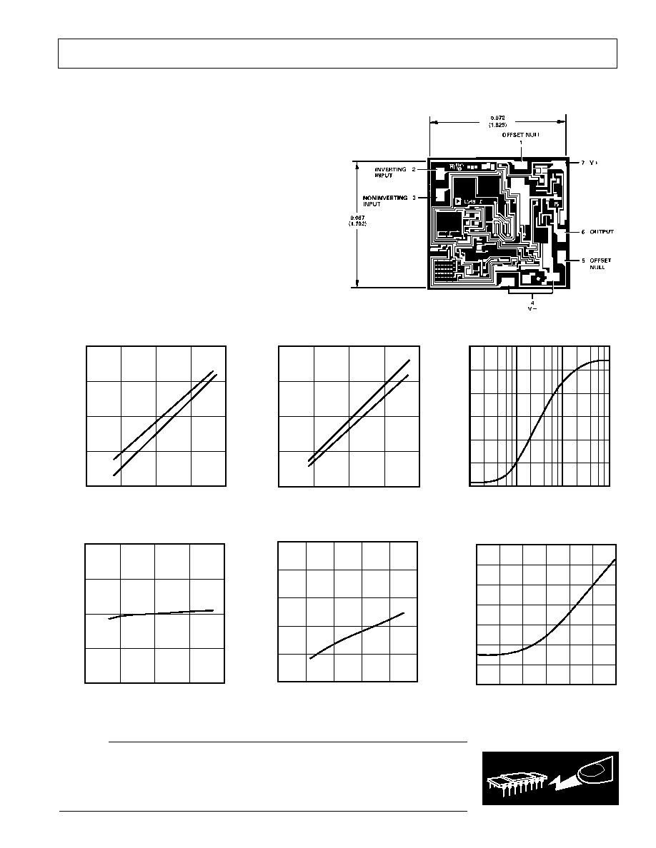
METALIZATION PHOTOGRAPH
Dimensions shown in inches and (mm).
Contact factory for latest dimensions
SUPPLY VOLTAGE
±
V
20
15
10
5
0
INPUT VOLTAGE
±
V
0 5 10 15 20
+V
IN
V
IN
Figure 1. Input Voltage Range
vs. Supply Voltage
SUPPLY VOLTAGE
±
V
200
180
160
140
120
QUIESCENT CURRENT µA
0 5 10 15 20
Figure 4. Quiescent Current vs.
Supply Voltage
SUPPLY VOLTAGE
±
V
10
6
4
2
0
INPUT BIAS CURRENT pA
0 4 8 12 16 20
8
Figure 5. Input Bias Current
vs. Supply Voltage
Typical Characteristics
LOAD RESISTANCE
30
25
20
10
0
10 100 1k 10k
5
15
OUTPUT VOLTAGE SWING Volts p-p
Figure 3. Output Voltage Swing
vs. Load Resistance
SUPPLY VOLTAGE
±
V
20
15
10
5
0
OUTPUT VOLTAGE SWING
±
V
0 5 10 15 20
+V
OUT
V
OUT
25
°
C
R
L
= 10k
Figure 2. Output Voltage Swing
vs. Supply Voltage
TEMPERATURE
°
C
100nA
INPUT BIAS CURRENT
55 25 5 35 65 95 125
10nA
1nA
100pA
10pA
1pA
100fA
10fA
Figure 6. Input Bias Current vs.
Temperature
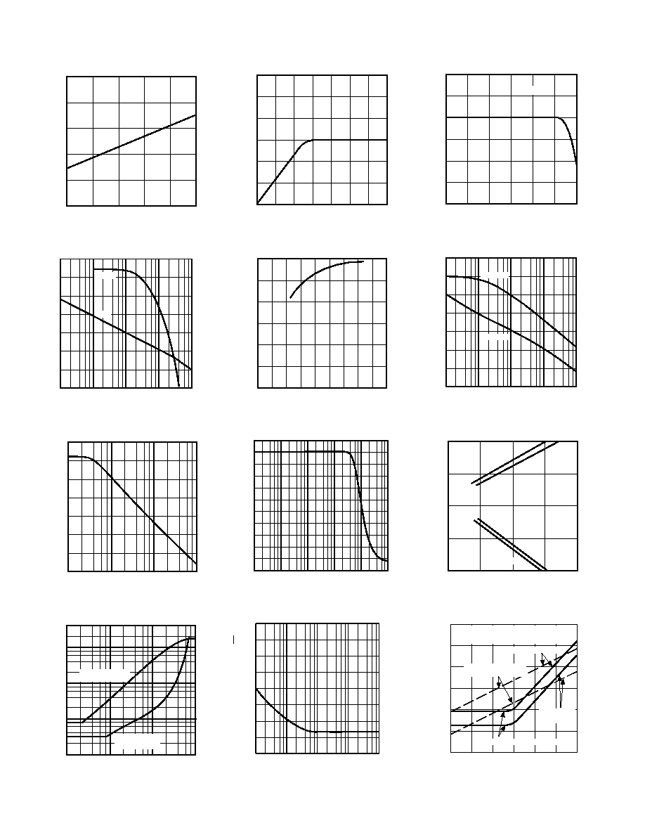
COMMON-MODE VOLTAGE V
10
6
4
2
0
INPUT BIAS CURRENT pA
10 6 2 2 6 10
8
Figure 7. Input Bias Current vs.
Common-Mode Voltage
FREQUENCY Hz
100
80
60
0
40
1k 10k 100k 1M 10M
20
20
40
PHASE IN DEGREES
100
80
60
0
40
20
20
40
PHASE
GAIN
OPEN LOOP GAIN dB
Figure 10. Open Loop Frequency
Response
FREQUENCY Hz
90
80
70
50
20
1k 10k 100k 1M
40
60
CMRR dB
30
Figure 13. CMRR vs. Frequency
FREQUENCY Hz
4
1
0.001
100 1k 10k
0.01
0.1
TOTAL HARMONIC DISTORTION %
100k
FOLLOWER
WITH GAIN = 10
UNITY GAIN
FOLLOWER
Figure 16. Total Harmonic
Distortion vs. Frequency
AD548Typical Characteristics
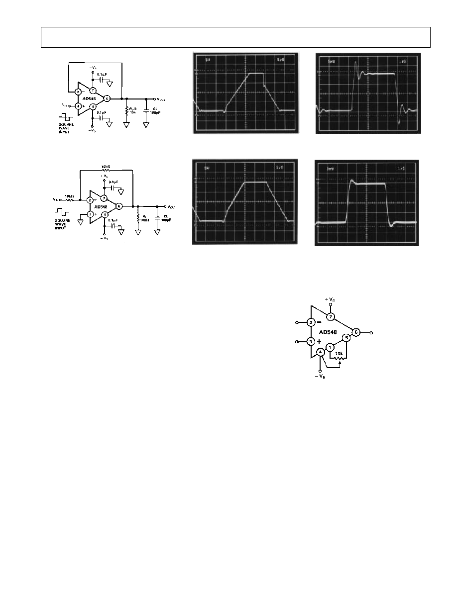
TEMPERATURE
°
C
1500
1000
750
500
0
55 25 5 35 65 95 125
1250
250
R
L
= 10k
OPEN LOOP GAIN V/mV
Figure 9. Open Loop Gain vs.
Temperature
FREQUENCY Hz
120
100
80
20
20
100 1k 10k 100k 1M
0
40
60
SUPPLY
+SUPPLY
POWER SUPPLY REJECTION dB
Figure 12. PSRR vs. Frequency
10mV
SETTLING TIME µs
10
0
5
10
OUTPUT VOLTAGE SWING V
0 2 4 6 8
5
1mV
1mV
10mV
Figure 15. Output Swing and Error
Voltage vs. Output Settling Time
SOURCE IMPEDANCE
1,000
100
10
0
100k 1M 10M 100M 1G 10G 100G
10,000
1
AMPLIFIER GENERATED NOISE
RESISTOR JOHNSON
NOISE
1kHz BANDWIDTH
10Hz
BANDWIDTH
WHENEVER JOHNSON NOISE IS GREATER THAN
AMPLIFIER NOISE, AMPLIFIER NOISE CAN BE
CONSIDERED NEGLIGIBLE FOR APPLICATION
INPUT NOISE VOLTAGE µV p-p
Figure 18. Total Noise vs. Source
Impedance
WARM-UP TIME Seconds
30
20
15
10
0
0 10 20 30 40 50 60 70
25
5
I
V
OS
I
µ
V
Figure 8. Change in Offset Voltage
vs. Warm-Up Time
SUPPLY VOLTAGE
±
V
120
100
90
80
60
OPEN LOOP VOLTAGE GAIN dB
0 2 4 6 8 10 12 14 16 18
110
70
Figure 11. Open Loop Voltage Gain
vs. Supply Voltage
OUTPUT VOLTAGE V p-p
FREQUENCY Hz
22
20
18
12
8
10 100 1k 10k 100k 1M
10
14
16
0
6
4
2
Figure 14. Large Signal Frequency
Response
FREQUENCY Hz
160
140
120
60
20
10 100 1k 10k 100k
40
80
100
0
INPUT NOISE VOLTAGE nV/
Hz
Figure 17. Input Noise Voltage
Spectral Density
4
REV. C
Typical CharacteristicsAD548
Figure 19c. Unity Gain Follower
Pulse Response (Small Signal)
Figure 19b. Unity Gain Follower
Pulse Response (Large Signal)
Figure 20c. Unity Gain Inverter
Pulse Response (Small Signal)
Figure 20b. Utility Gain Inverter
Pulse Response (Large Signal)
APPLICATION NOTES
The AD548 is a JFET-input op amp with a guaranteed maxi-
mum I
B
of less than 10 pA, and offset and drift laser-trimmed to
0.25 mV and 2
µ
V/
°
C respectively (AD548C). AC specs in-
clude 1 MHz bandwidth, 1.8 V/
µ
s typical slew rate and 8
µ
s set-
tling time for a 20 V step to
±
0.01%--all at a supply current less
than 200
µ
A. To capitalize on the device's performance, a num-
ber of error sources should be considered.
The minimal power drain and low offset drift of the AD548
reduce self-heating or "warm-up" effects on input offset voltage,
making the AD548 ideal for on/off battery powered applica-
tions. The power dissipation due to the AD548's 200
µ
A supply
current has a negligible effect on input current, but heavy out-
put loading will raise the chip temperature. Since a JFET's in-
put current doubles for every 10
°
C rise in chip temperature, this
can be a noticeable effect.
The amplifier is designed to be functional with power supply
voltages as low as
±
4.5 V. It will exhibit a higher input offset
voltage than at the rated supply voltage of
±
15 V, due to power
supply rejection effects. The common-mode range of the
AD548 extends from 3 V more positive than the negative supply
to 1 V more negative than the positive supply. Designed to
cleanly drive up to 10 k
and 100 pF loads, the AD548 will
drive a 2 k
load with reduced open loop gain.
OFFSET NULLING
Unlike bipolar input amplifiers, zeroing the input offset voltage
of a BiFET op amp will not minimize offset drift. Using balance
Pins 1 and 5 to adjust the input offset voltage as shown in Fig-
ure 21 will induce an added drift of 0.24
µ
V/
°
C per 100
µ
V of
nulled offset. The low initial offset (0.25 mV) of the AD548C
results in only 0.6
µ
V/
°
C of additional drift.
REV. C
5
Figure 19a. Unity Gain Follower
Figure 20a. Utility Gain Inverter
Applying the AD548
Figure 21. Offset Null Configuration
LAYOUT
To take full advantage of the AD548's 10 pA max input current,
parasitic leakages must be kept below an acceptable level. The
practical limit of the resistance of epoxy or phenolic circuit
board material is between 1
×
10
12
and 3
×
10
12
. This can
result in an additional leakage of 5 pA between an input of 0 V
and a 15 V supply line. Teflon or a similar low leakage material
(with a resistance exceeding 10
17
) should be used to isolate
high impedance input lines from adjacent lines carrying high
voltages. The insulator should be kept clean, since contaminants
will degrade the surface resistance.
A metal guard completely surrounding the high impedance
nodes and driven by a voltage near the common-mode input po-
tential can also be used to reduce some parasitic leakages. The
guarding pattern in Figure 22 will reduce parasitic leakage due
to finite board surface resistance; but it will not compensate for
a low volume resistivity board.
AD548
6
REV. C
Figure 22. Board Layout for Guarding Inputs
INPUT PROTECTION
The AD548 is guaranteed to withstand input voltages equal to
the power supply potential. Exceeding the negative supply volt-
age on either input will forward bias the substrate junction of
the chip. The induced current may destroy the amplifier due to
excess heat.
Input protection is required in applications such as a flame
detector in a gas chromatograph, where a very high potential
may be applied to the input terminals during a sensor fault con-
dition. Figure 23 shows a simple current limiting scheme that
can be used. R
PROTECT
should be chosen such that the maxi-
mum overload current is 1.0 mA (l00 k
for a 100 V overload,
for example).
Exceeding the negative common-mode range on either input
terminal causes a phase reversal at the output, forcing the
amplifier output to the corresponding high or low state. Exceed-
ing the negative common-mode on both inputs simultaneously
forces the output high. Exceeding the positive common-mode
range on a single input doesn't cause a phase reversal, but if
both inputs exceed the limit the output will be forced high. In
all cases, normal amplifier operation is resumed when input
voltages are brought back within the common-mode range.
Figure 23. Input Protection of IV Converter
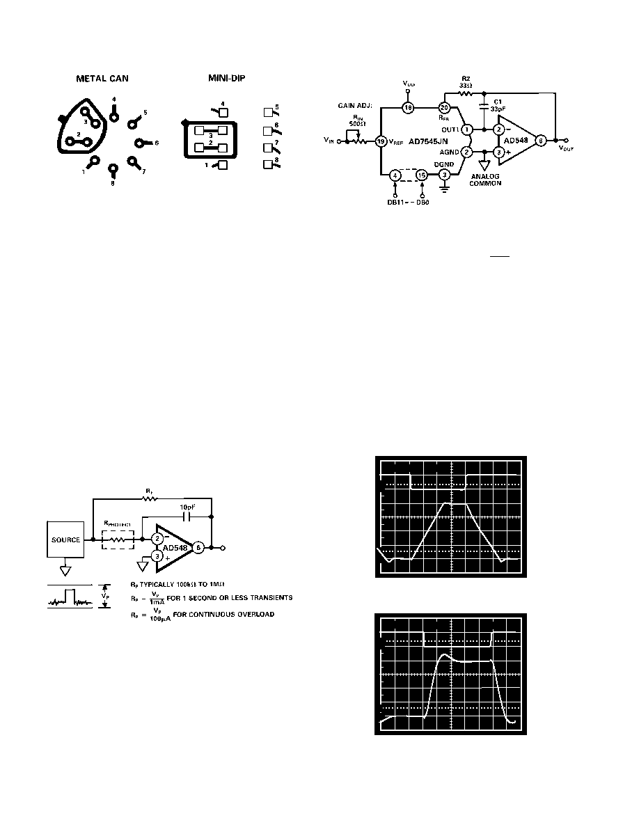
D/A CONVERTER OUTPUT BUFFER
The circuit in Figure 24 shows the AD548 and AD7545 12-bit
CMOS D/A converter in a unipolar binary configuration. V
OUT
will be equal to V
REF
attenuated by a factor depending on the
digital word. V
REF
sets the full scale. Overall gain is trimmed by
adjusting R
IN
. The AD548's low input offset voltage, low drift
and clean dynamics make it an attractive low power output
buffer.
The input offset voltage of the AD548 output amplifier results
in an output error voltage. This error voltage equals the input
offset voltage of the op amp times the noise gain of the
amplifier.
Figure 24. AD548 Used as DAC Output Amplifier
That is:
V
OS
Output
=
V
OS
Input 1
+
R
FB
R
O
R
FB
is the feedback resistor for the op amp, which is internal to
the DAC. R
O
is the DAC's R-2R ladder output resistance. The
value of R
O
is code dependent. This has the effect of changing
the offset error voltage at the amplifier's output. An output am-
plifier with a sub millivolt input offset voltage is needed to
preserve the linearity of the DAC's transfer function.
The AD548 in this configuration provides a 700 kHz small sig-
nal bandwidth and 1.8 V/
µ
s typical slew rate. The 33 pF capaci-
tor across the feedback resistor optimizes the circuit's response.
The oscilloscope photos in Figures 25 and 26 show small and
large signal outputs of the circuit in Figure 24. Upper traces
show the input signal V
IN
. Lower traces are the resulting output
voltage with the DAC's digital input set to all 1s. The AD548
settles to
±
0.01% for a 20 V input step in 14
µ
s.
0%
10
5V
5µS
20V
100
90
Figure 25. Response to
±
20 V p-p Reference Square Wave
0%
10
50mV
2µS
200mV
100
90
Figure 26. Response to
±
100 mV p-p Reference Square
Wave
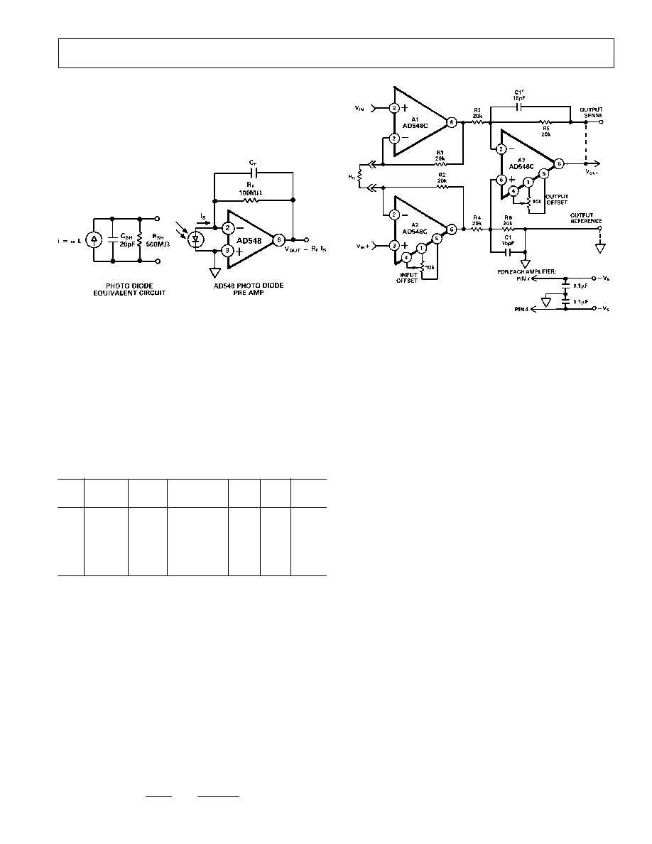
Figure 29. Low Power Instrumentation Amplifier
Gains of 1 to 100 can be accommodated with gain nonlinearities
of less than 0.01%. Referred to input errors, which contribute
an output error proportional to in amp gain, include a maxi-
mum untrimmed input offset voltage of 0.5 mV and an input
offset voltage drift over temperature of 4
µ
V/
°
C. Output errors,
which are independent of gain, will contribute an additional
0.5 mV offset and 4
µ
V/
°
C drift. The maximum input current is
15 pA over the common-mode range, with a common-mode
impedance of over 1
×
10
12
. Resistor pairs R3/R5 and R4/R6
should be ratio matched to 0.01% to take full advantage of the
AD548's high common-mode rejection. Capacitors C1 and C1
compensate for peaking in the gain over frequency caused by
input capacitance when gains of 1 to 3 are used.
The 3 dB small signal bandwidth for this low power instru-
mentation amplifier is 700 kHz for a gain of 1 and 10 kHz for a
gain of 100. The typical output slew rate is 1.8 V/
µ
s.
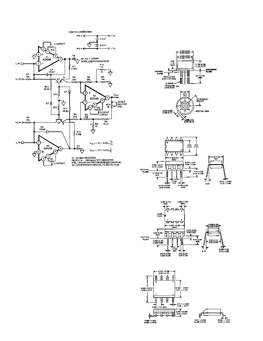
LOG RATIO AMPLIFIER
Log ratio amplifiers are useful for a variety of signal condition-
ing applications, such as linearizing exponential transducer out-
puts and compressing analog signals having a wide dynamic
range. The AD548's picoamp level input current and low input
offset voltage make it a good choice for the front-end amplifier
of the log ratio circuit shown in Figure 30. This circuit produces
an output voltage equal to the log base 10 of the ratio of the in-
put currents I
1
and I
2
. Resistive inputs R1 and R2 are provided
for voltage inputs.
Input currents I
1
and I
2
set the collector currents of Q1 and Q2,
a matched pair of logging transistors. Voltages at points A and
B are developed according to the following familiar diode
equation:
V
BE
=
(kT/q) ln (I
C
/I
ES
)
In this equation, k is Boltzmann's constant, T is absolute tem-
perature, q is an electron charge, and I
ES
is the reverse saturation
current of the logging transistors. The difference of these two
voltages is taken by the subtractor section and scaled by a factor
of approximately 16 by resistors R9, R10, and R8. Temperature
Application HintsAD548
PHOTODIODE PREAMP
The performance of the photodiode preamp shown in Figure 27
is enhanced by the AD548's low input current, input voltage
offset and offset voltage drift. The photodiode sources a current
proportional to the incident light power on its surface. R
F
converts
the photodiode current to an output voltage equal to R
F
×
I
S
.
Figure 27.
An error budget illustrating the importance of low amplifier
input current, voltage offset and offset voltage drift to minimize
output voltage errors can be developed by considering the equi-
valent circuit for the small (0.2 mm
2
area) photodiode shown in
Figure 27. The input current results in an error proportional to
the feedback resistance used. The amplifier's offset will produce
an error proportional to the preamp's noise gain (I + R
F
/R
SH
),
where R
SH
is the photodiode shunt resistance. The amplifier's
input current will double with every 10
°
C rise in temperature,
and the photodiode's shunt resistance halves with every 10
°
C
rise. The error budget in Figure 28 assumes a room temperature
photodiode R
SH
of 500 M
, and the maximum input current
and input offset voltage specs of an AD548C.
TEMP
C
R
SH
(M )
V
OS
( V) (1+ R
F
/R
SH
) V
OS
I
B
(pA)
I
B
R
F
TOTAL
25
15,970
150
151
µ
V
0.30
30
µ
V
181
µ
V
0
2,830
200
207
µ
V
2.26
262
µ
V 469
µ
V
+25
500
250
300
µ
V
10.00
1.0 mV 1.30 mV
+50
88.5
300
640
µ
V
56.6
5.6 mV 6.24 mV
+75
15.6
350
2.6 mV
320
32 mV
34.6 mV
+85
7.8
370
5.1 mV
640
64 mV
69.1 mV
Figure 28. Photo Diode Pre-Amp Errors Over Temperature
The capacitance at the amplifier's negative input (the sum of the
photodiode's shunt capacitance, the op amp's differential input
capacitance, stray capacitance due to wiring, etc.) will cause a
rise in the preamp's noise gain over frequency. This can result in
excess noise over the bandwidth of interest. C
F
reduces the
noise gain "peaking" at the expense of bandwidth.
INSTRUMENTATION AMPLIFIER
The AD548C's maximum input current of 10 pA makes it an
excellent building block for the high input impedance instru-
mentation amplifier shown in Figure 29. Total current drain for
this circuit is under 600
µ
A. This configuration is optimal for
conditioning differential voltages from high impedance sources.
The overall gain of the circuit is controlled by R
G
, resulting in
the following transfer function:
V
OUT
V
IN
=
1
+
( R
1
+
R
2
)
R
G
REV. C
7
AD548
8
REV. C
PRINTED IN U.S.A.
C999a1912/86
OUTLINE DIMENSIONS
Dimensions shown in inches and (mm).
Figure 30. Log Ratio Amplifier
compensation is provided by resistors R8 and R15, which have a
positive 3500 ppm/
°
C temperature coefficient. The transfer
function for the output voltage is:
V
OUT
=
1V log
10
( I
2
/ I
1
)
Frequency compensation is provided by R11, R12, C1, and C2.
Small signal bandwidth is approximately 300 kHz at input cur-
rents above 100
µ
A and will proportionally decrease with lower
signal levels. D1, D2, R13, and R14 compensate for the effects
of the two logging transistors' ohmic emitter resistance.
To trim this circuit, set the two input currents to 10
µ
A and ad-
just V
OUT
to zero by adjusting the potentiometer on A3. Then
set I
2
to 1
µ
A and adjust the scale factor such that the output
voltage is 1 V by trimming potentiometer R10. Offset adjust-
ment for A1 and A2 is provided to increase the accuracy of the
voltage inputs.
This circuit ensures a 1% log conformance error over an input
current range of 300 pA to 1 mA, with low level accuracy
limited by the AD548's input current. The low level input volt-
age accuracy of this circuit is limited by the input offset voltage
and drift of the AD548.
TO-99 (H) Package
SOIC (R) Package
Plastic Mini-DIP (N) Package
Cerdip (Q) Package