 | ÐлекÑÑоннÑй компоненÑ: AD5520JST | СкаÑаÑÑ:  PDF PDF  ZIP ZIP |
Äîêóìåíòàöèÿ è îïèñàíèÿ www.docs.chipfind.ru
REV. A
Information furnished by Analog Devices is believed to be accurate and
reliable. However, no responsibility is assumed by Analog Devices for its
use, nor for any infringements of patents or other rights of third parties that
may result from its use. No license is granted by implication or otherwise
under any patent or patent rights of Analog Devices. Trademarks and
registered trademarks are the property of their respective owners.
One Technology Way, P.O. Box 9106, Norwood, MA 02062-9106, U.S.A.
Tel: 781/329-4700
www.analog.com
Fax: 781/326-8703
© 2003 Analog Devices, Inc. All rights reserved.
AD5520
Per Pin Parametric
Measurement Unit/Source Measure Unit
FEATURES
Force/Measure Functions
Force Voltage/Current, Measure Current/Voltage
Force Current/Voltage, Measure Current/Voltage
Force/Measure Voltage Range 11 V
4 Programmable Force/Measure Current Ranges
4 A, 40 A, 400 A, 4 mA
Extended Current Ranges
40 mA and 160 mA with External Driver
Clamp Circuitry and Window Comparators On Board
Guard Amplifier
64-Lead LQFP Package
APPLICATIONS
Automatic Test Equipment
Per Pin PMU, Shared Pin PMU, Device Power Supply
Instrumentation
Source Measure, Parametric Measurement, Precision
Measurement
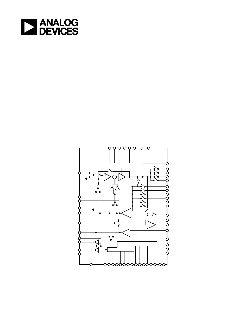
FUNCTIONAL BLOCK DIAGRAM
CLLDETECT
MEASI4H
FIN
BW SELECT
COMPOUT2
FOH1
FOH2
FOH3
FOH0
AV
EE
AV
CC
CLH
CLL
REFGND
MEASIOUT
MEASOUT
MEASVOUT
G = 16
G = 1
CPH
CPOH
CPOH
CPL
MEASI5H
MEASIL
GUARDIN
GUARD
MEASVH
MEASVL
AGND
QM5
QM4
DGND
DV
DD
CS
STANDBY
COMPOUT1
COMPOUT0
COMPIN2
COMPIN1
COMPIN0
CLAMP
DETECT
V
SENSE
INST AMP
I
SENSE
INST AMP
LOGICS
AC0
AC1
CLHDETECT
MOE
AM0
AM1
AM2
MSEL
FSEL
CPSEL
STB
CPCK
AD5520
COMPARATOR
G = 1
FOH
MEASI3H
MEASI2H
MEASI1H
MEASI0H
GENERAL DESCRIPTION
The AD5520 is a single channel per pin parametric measure-
ment unit (PPMU) for use in semiconductor automatic test
equipment. The part is also suited for use as a source
measurement unit for instrumentation applications. It
contains programmable modes to force a pin voltage and
measure the corresponding current or force a current and
measure the voltage. The AD5520 can force/measure over a
±11 V range or currents up to ±4 mA with its on-board
force amplifier. An external amplifier is required for wider
current ranges. The device provides a force sense capability to
ensure accuracy at the tester pin. A guard output is also
available to drive the shield of a force/sense pair. The AD5520
is available in a 64-lead LQFP package.

REV. A
2
AD5520SPECIFICATIONS
(AV
CC
= +15 V
5%, AV
EE
= 15 V
5%, DV
DD
= 5 V
10%, AGND = 0 V, REFGND = 0 V,
DGND = 0 V. All specifications 0 C to 70 C, unless otherwise noted.)
Parameter
Min
Typ
1
Max
Unit
Test Conditions/Comments
VOLTAGE FORCE MODE
Force Control Output Voltage Range
11
V
R
LOAD
= 10 k
, C
LOAD
= 50 pF
FOH Output Impedance
70
FOH0
2.5
k
FOH1
3
k
FOH2
500
FOH3
60
Input Offset Error
1
5
mV
Gain Error
1
%
Clamp Voltage Error
2
1
% FS
of FIN
CURRENT MEASURE/FORCE
Set with external sense resistors
FOH0
±4
µA
MODE0, R
S
= 125 k
FOH1
±40
µA
MODE1, R
S
= 12.5 k
FOH2
±400
µA
MODE2, R
S
= 12.5 k
FOH3
±4
mA
MODE3, R
S
= 125
CURRENT MEASURE MODE
High Sense Input Range, V
MEASIxH
11
V
Linearity
3
0.01
% FSR
+11 V > V
FOL
> 11 V
Input Bias Current
1
3
nA
Input Bias Current Drift
1
50
pA/
°C
Output Offset Error
100
mV
MODE0
100
mV
MODE1
100
mV
MODE2
100
mV
MODE3
Gain Error
0.1
0.35
%
Gain of 16
Gain Error Temperature Coefficient
4
30
µV/°C
MEASIOUT Output Load Current
4
mA
CMRR
95
dB
@ DC
CURRENT FORCE MODE
Input Offset Error
10
mV
With MODE0, MODE1, MODE2, MODE3
Gain Error
1
%
Clamp Current Error
2
1
% FS
of FIN
VOLTAGE MEASURE MODE
Differential Input Range
11
V
Low Sense Input Voltage Range
100
mV
MEASVL
Linearity
3
+0.005
% FSR
+11 V > V
MEASVH
to V
MEASVL
> 11 V
Input Offset Error
5
10
mV
FIN = 0 V, Measured @ MEASVOUT
Input Offset Error Temperature
Coefficient
1
15
mV/
°C
Gain Error
0.03
0.15
%
Gain of 1
Gain Error Temperature Coefficient
4
2
mV/
°C
Input Bias Current
1
3
nA
Input Bias Current Drift
4
50
pA/
°C
MEASVOUT Output Load Current
4
mA
CMRR
4
73
dB
@ DC
AMPLIFIER SETTLING TIME
4, 5
V
SENSE
Amp
20
µs
To 0.2%
I
SENSE
Amp
12
µs
To 0.2%
LOOP SETTLING
4, 5
Settling to within 0.024% of 8 V step
COMPIN2 = 100 pF
450
600
µs
MODE0
285
390
µs
MODE1
170
240
µs
MODE2, MODE3
COMPIN1 = 1000 pF
2
2.5
ms
MODE0
1.8
2.4
ms
MODE1, MODE2, MODE3
COMPIN0 = 3000 pF
5.75
8.7
ms
MODE0, MODE1, MODE2, MODE3

REV. A
AD5520
3
Parameter
Min
Typ
1
Max
Unit
Test Conditions/Comments
SLEW RATE
4, 5
50
mV/
µs
COMPIN2 = 100 pF
4.3
mV/
µs
COMPIN1 = 1000 pF
1.28
mV/
µs
COMPIN0 = 3000 pF
COMPARATOR
CPH, CPL Input Range
11
V
V
CPH
> V
CPL
Input Offset
7
mV
GUARD DRIVER
Output Voltage
11
V
Output Impedance
130
Capacitive Load Only
Output Offset Voltage
400
mV
Load Current
4
4
mA
Output Settling Time
4
0.5
2
µs
100 pF Capacitive Load
ANALOG REFERENCE INPUTS
Force Control Input Range
11
V
Force Control Input Impedance
1
M
Clamp Control Input Range
11
V
V
CLH
> V
CLL
Clamp Control Input Impedance
1
M
Comparator Threshold Input Range
11
V
Comparator Threshold Input Impedance
1
M
Input Capacitance
4
3
pF
ANALOG MEASUREMENT OUTPUTS
Voltage Measure Output Impedance
2
Current Measure Output Impedance
3
Multiplexed Sense Output Impedance
1
k
Input Capacitance
MEASIxH, MEASVH, FOHx
8
pF
LOGIC INPUTS
Input Current
1
µA
All digital inputs together
Input Low Voltage, V
INL
0.8
V
Input High Voltage, V
IHL
2.0
V
Input Capacitance
4
3
pF
LOGIC OUTPUTS
Output Low Voltage, V
OL
4
0.4
V
I
SINK
= 2 mA
Output High Voltage, V
OH
4
2.4
V
I
SOURCE
= 2 mA
POWER REQUIREMENTS
AV
CC
+14.25
+15
+15.75
V
For specific performance
6
AV
EE
14.25
15
+15.75
V
Power Supply Rejection Ratio, PSRR
1
FOH
25
dB
100 kHz
16
dB
500 kHz
15
dB
1 MHz
MEASOUT
55
dB
100 kHz
10
dB
500 kHz
DC PSR
90
dB
DV
DD
5
V
I
AVCC
12
mA
I
AVEE
12
mA
I
DVDD
0.5
mA
Digital inputs at supply rails
NOTES
1
Typical values are at 25
°C and nominal supply, unless otherwise noted.
2
Full-scale = 11 V.
3
Full-scale range = 22 V.
4
Guaranteed by design and characterization but not subject to production test.
5
Force control amplifier dominates slew rate and settling time.
6
Operational with
±12 V supplies, force/measure range is reduced to ± 8.5 V.
Specifications subject to change without notice.
REV. A
4
AD5520
TIMING CHARACTERISTICS
1, 2
(AV
CC
= +15 V
5%, AV
EE
= 15 V
5%, AGND = 0 V, REFGND = 0 V, DGND = 0 V. All
specifications 0 C to 70 C, unless otherwise noted.)
DV
DD
Parameter
5 V
10%
3.3 V
Unit
Conditions/Comments
t
1
0
0
ns min
CS Falling Edge to STB Falling Edge Setup Time
t
2
30
200
ns min
STB Pulse Width
t
3
40
70
ns min
STB Rising Edge to CS Rising Edge Setup Time
t
4
0
40
ns min
Data Setup Time
t
5
550
560
ns min
CS Falling Edge to CPCK Rising Edge Setup Time
t
6
320
320
ns min
CPCK Pulse Width
t
7
450
500
ns min
CPCK to
STB Falling Edge Setup Time
t
8
150
800
ns min
STB Rising Edge to QMx, CLxDETECT Valid
t
9
100
440
ns min
STB Rising Edge to CPOH, CPOL Valid
t
10
240
240
µs min
Comparator Setup Time, MODE2, MODE3 settling
t
11
150
500
ns min
Comparator Hold Time
t
12
100
440
ns min
Comparator Output Delay Time
t
13
320
320
ns min
Comparator Strobe Pulse Width
NOTES
1
See Figure 1.
2
All input signals are specified with tr = tf = 1 ns (10% to 90% of V
DD
) and timed from a voltage level of (V
IL
+ V
IH
)/2.
Specifications subject to change without notice.
t
11
t
10
t
13
t
12
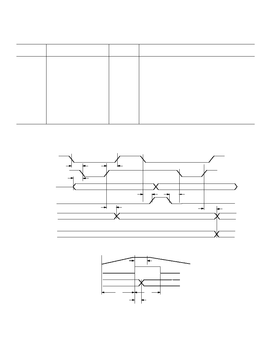
CPCK
CPOH, CPOL
MEASVOUT
OR MEASIOUT
Figure 2. Comparator Timing
CPCK
AMx, ACx, FSEL,
MSEL, CPSEL
CS
QM4, QM5,
CLHDETECT,
CLLDETECT
CPOL, CPOH
STB
t
3
t
2
t
1
t
4
t
5
t
6
t
7
t
8
t
9
Figure 1. Timing Diagram
REV. A
AD5520
5
ABSOLUTE MAXIMUM RATINGS
*
(T
A
= 25
°C, unless otherwise noted.)
AV
CC
to AV
EE
. . . . . . . . . . . . . . . . . . . . . . . . . . . . . . . . . 34 V
AV
CC
to AGND . . . . . . . . . . . . . . . . . . . . . . . . . 0.3 V, +17 V
AV
EE
to AGND . . . . . . . . . . . . . . . . . . . . . . . . . +0.3 V, 17 V
DV
DD
. . . . . . . . . . . . . . . . . . . . . . . . . . . . . . . . 0.3 V to +6 V
Digital Inputs to DGND . . . . . . . . . . 0.3 V to DV
DD
+ 0.3 V
Analog Inputs to AGND . . . . . AV
CC
+ 0.3 V to AV
EE
0.3 V
C
LH
to C
LL
. . . . . . . . . . . . . . . . . . . . . . . . . . . . 0.3 V to +34 V
C
PH
to C
PL
. . . . . . . . . . . . . . . . . . . . . . . . . . . . 0.3 V to +34 V
REFGND, DGND . . . . . . . . . AV
CC
+ 0.3 V to AV
EE
0.3 V
Operating Temperature Range
Commercial (J Version) . . . . . . . . . . . . . . . . . . 0
°C to 70°C
Storage Temperature Range . . . . . . . . . . . . 65
°C to +150°C
Maximum Junction Temperature, (T
J
max) . . . . . . . . . 150
°C
Package Power Dissipation . . . . . . . . . . . . . (T
J
max T
A
)/
JA
Thermal Impedance
JA
. . . . . . . . . . . . . . . . . . . . . . 47.8
°C/W
Lead Temperature (Soldering 10 sec) . . . . . . . . . . . . . . 300
°C
IR Reflow, Peak Temperature . . . . . . . . . . . . . . . . . . . . 220
°C
*Stresses above those listed under Absolute Maximum Ratings may cause perma-
nent damage to the device. This is a stress rating only; functional operation of the
device at these or any other conditions above those listed in the operational
sections of this specification is not implied. Exposure to absolute maximum rating
conditions for extended periods may affect device reliability.
CAUTION
ESD (electrostatic discharge) sensitive device. Electrostatic charges as high as 4000 V readily
accumulate on the human body and test equipment and can discharge without detection. Although the
AD5520 features proprietary ESD protection circuitry, permanent damage may occur on devices
subjected to high energy electrostatic discharges. Therefore, proper ESD precautions are recommended
to avoid performance degradation or loss of functionality.
ORDERING GUIDE
Model
Temperature Range
Package Description
Package Option
AD5520JST
0
°C to 70°C
64-Lead LQFP
ST-64-2
AD5520JST-REEL
0
°C to 70°C
64-Lead LQFP
ST-64-2
EVAL-AD5520EB
Evaluation Board and Software
Document Outline
- FEATURES
- APPLICATIONS
- GENERAL DESCRIPTION
- FUNCTIONAL BLOCK DIAGRAM
- SPECIFICATIONS
- TIMING CHARACTERISTICS
- ABSOLUTE MAXIMUM RATINGS
- ORDERING GUIDE
- PIN CONFIGURATION
- PIN FUNCTION DESCRIPTIONS
- Typical Performance Characteristics
- THEORY OF OPERATION
- INTERFACE
- Standby Mode
- Force Voltage or Force Current
- Measured Parameter
- Current Ranges
- RS Selection
- Force Control Amplifier
- Comparator Function and Strobing
- Clamp Function
- High Current Ranges
- CIRCUIT OPERATION
- Force Voltage
- Measure Current
- Force Current
- Measure Voltage
- Short Circuit Protection
- SETTLING TIME CONSIDERATIONS
- PCB LAYOUT AND POWER SUPPLY DECOUPLING
- TYPICAL CONNECTION CIRCUIT FOR THE AD5520
- TYPICAL APPLICATION CIRCUIT
- EVALUATION BOARD FOR THE AD5520 PMU
- OUTLINE DIMENSIONS
- Revision History