Äîêóìåíòàöèÿ è îïèñàíèÿ www.docs.chipfind.ru
REV. 0
Information furnished by Analog Devices is believed to be accurate and
reliable. However, no responsibility is assumed by Analog Devices for its
use, nor for any infringements of patents or other rights of third parties
which may result from its use. No license is granted by implication or
otherwise under any patent or patent rights of Analog Devices.
a
AD5533*
One Technology Way, P.O. Box 9106, Norwood, MA 02062-9106, U.S.A.
Tel: 781/329-4700
World Wide Web Site: http://www.analog.com
Fax: 781/326-8703
© Analog Devices, Inc., 2000
*Protected by U.S. Patent No. 5,969,657; other patents pending.
32-Channel Infinite
Sample-and-Hold
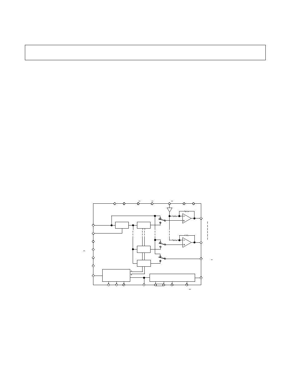
FUNCTIONAL BLOCK DIAGRAM
SYNC/CS
WR
CAL
A4 A0
SCLK
OFFSET SEL
AD5533
DV
CC
V
IN
D
IN
D
OUT
ADDRESS INPUT REGISTER
AV
CC
REF IN
REF OUT
OFFS IN
INTERFACE
CONTROL
LOGIC
OFFS OUT
V
OUT
31
V
OUT
0
TRACK / RESET
BUSY
DAC GND
AGND
DGND
SER /
PAR
V
DD
V
SS
DAC
DAC
DAC
ADC
FEATURES
Infinite Sample-and-Hold Capability to 0.018% Accuracy
High Integration: 32-Channel SHA in 12 12 mm
2
LFBGA
Per Channel Acquisition Time of 16 s max
Adjustable Voltage Output Range
Output Voltage Span 10 V
Output Impedance 0.5
Readback Capability
DSP-/Microcontroller-Compatible Serial Interface
Parallel Interface
Temperature Range 40 C to +85 C
APPLICATIONS
Level Setting
Instrumentation
Automatic Test Equipment
Industrial Control Systems
Data Acquisition
Low Cost I/O
GENERAL DESCRIPTION
The AD5533 combines a 32-channel voltage translation function
with an infinite output hold capability. An analog input voltage
on the common input pin, V
IN
, is sampled and its digital repre-
sentation transferred to a chosen DAC register. V
OUT
for this
DAC is then updated to reflect the new contents of the DAC
register. Channel selection is accomplished via the parallel address
inputs A0A4 or via the serial input port. The output voltage
range is determined by the offset voltage at the OFFS_IN pin
and the gain of the output amplifier. It is restricted to a range
from V
SS
+ 2 V to V
DD
2 V because of the headroom of the
output amplifier.
The device is operated with AV
CC
= 5 V
± 5%, DV
CC
= 2.7 V to
5.25 V, V
SS
= 4.75 V to 16.5 V and V
DD
= 8 V to 16.5 V and
requires a stable 3 V reference on REF_IN as well as an offset
voltage on OFFS_IN.
PRODUCT HIGHLIGHTS
1. Infinite Droopless Sample-and-Hold Capability.
2. The AD5533 is available in a 74-lead LFBGA package with a
body size of 12 mm
× 12 mm.

2
REV. 0
AD5533SPECIFICATIONS
(V
DD
= 8 V to 16.5 V, V
SS
= 4.75 V to 16.5 V; AV
CC
= 4.75 V to 5.25 V; DV
CC
= 2.7 V
to 5.25 V; AGND = DGND = DAC_GND = 0 V; REF_IN = 3 V; Output Range from
V
SS
+ 2 V to V
DD
2 V. All outputs unloaded. All specifications T
MIN
to T
MAX
unless otherwise noted.)
Parameter
1
A Version
2
Unit
Conditions/Comments
ANALOG CHANNEL
V
IN
to V
OUT
Nonlinearity
±0.018
% max
Input Range 100 mV to 2.96 V
±0.006
% typ
After Gain and Offset Adjustment
Gain
3.46/3.6
min/max
3.52 typ
Offset Error
±50
mV max
ANALOG INPUT (V
IN
)
Input Voltage Range
0 to 3
V
Nominal Input Range
Input Lower Deadband
70
mV max
50 mV typ. Referred to V
IN
.
See Figure 5
Input Upper Deadband
40
mV max
12 mV typ. Referred to V
IN
.
See Figure 5
Input Current
1
µA max
100 nA typ. V
IN
Being Acquired on
One Channel
Input Capacitance
3
20
pF typ
ANALOG INPUT (OFFS_IN)
Input Current
1
µA max
100 nA typ
VOLTAGE REFERENCE
REF_IN
Nominal Input Voltage
3.0
V
Input Voltage Range
3
2.85/3.15
V min/max
Input Current
1
µA max
<1 nA typ
REF_OUT
Output Voltage
3
V typ
Output Impedance
3
280
k
typ
Reference Temperature Coefficient
3
60
ppm/
°C typ
ANALOG OUTPUTS (V
OUT
031)
Output Temperature Coefficient
3,
4
20
ppm/
°C typ
DC Output Impedance
0.5
typ
Output Range
V
SS
+ 2 /V
DD
2
V min/max
100
µA Output Load
Resistive Load
3,
5
5
k
min
Capacitive Load
3, 5
500
pF max
Short-Circuit Current
3
10
mA typ
DC Power Supply Rejection Ratio
3
70
dB typ
V
DD
= +15 V
± 5%
70
dB typ
V
SS
= 15 V
± 5%
DC Crosstalk
3
250
µV max
ANALOG OUTPUT (OFFS_OUT)
Output Temperature Coefficient
3, 4
20
ppm/
°C typ
DC Output Impedance
3
1.3
k
typ
Output Range
50 to REF_IN 12
mV typ
Output Current
10
µA max
Source Current
Capacitive Load
100
pF max
DIGITAL INPUTS
3
Input Current
±10
µA max
5
µA typ
Input Low Voltage
0.8
V max
DV
CC
= 5 V
± 5%
0.4
V max
DV
CC
= 3 V
± 10%
Input High Voltage
2.4
V min
DV
CC
= 5 V
± 5%
2.0
V min
DV
CC
= 3 V
± 10%
Input Hysteresis (
SCLK and CS Only)
200
mV typ
Input Capacitance
10
pF max
DIGITAL OUTPUTS (
BUSY, DOUT)
3
Output Low Voltage
0.4
V max
DV
CC
= 5 V. Sinking 200
µA
Output High Voltage
4.0
V min
DV
CC
= 5 V. Sourcing 200
µA
Output Low Voltage
0.4
V max
DV
CC
= 3 V. Sinking 200
µA
Output High Voltage
2.4
V min
DV
CC
= 3 V. Sourcing 200
µA
High Impedance Leakage Current
±1
µA max
D
OUT
Only
High Impedance Output Capacitance
15
pF typ
D
OUT
Only
3
REV. 0
AD5533
(V
DD
= 8 V to 16.5 V, V
SS
= 4.75 V to 16.5 V; AV
CC
= 4.75 V to 5.25 V; DV
CC
= 2.7 V to 5.25 V; AGND =
DGND = DAC_GND = 0 V; REF_IN = 3 V; Output Range from V
SS
+ 2 V to V
DD
2 V. All outputs unloaded.
All specifications T
MIN
to T
MAX
unless otherwise noted.)
Parameter
A Version
1
Unit
Conditions/Comments
Output Settling Time
2
3
µs max
Acquisition Time
16
µs max
OFFS_IN Settling Time
2
10
µs max
500 pF, 5 k
Load; 0 V3 V Step
Digital Feedthrough
2
0.2
nV-s typ
Output Noise Spectral Density @ 1 kHz
2
400
nV/(
Hz)
typ
AC Crosstalk
2
5
nV-s typ
NOTES
1
A version: Industrial temperature range 40
°C to +85°C; typical at 25°C.
2
Guaranteed by design and characterization, not production tested
Specifications subject to change without notice.
Parameter
1
A Version
2
Unit
Conditions/Comments
POWER REQUIREMENTS
Power-Supply Voltages
V
DD
8/16.5
V min/max
V
SS
4.75/16.5
V min/max
AV
CC
4.75/5.25
V min/max
DV
CC
2.7/5.25
V min/max
Power-Supply Currents
6
I
DD
15
mA max
10 mA typ. All Channels Full Scale
I
SS
15
mA max
10 mA typ. All Channels Full Scale
AI
CC
33
mA max
26 mA typ
DI
CC
1.5
mA max
1 mA typ
Power Dissipation
6
280
mW typ
V
DD
= +10 V, V
SS
= 5 V
NOTES
1
See Terminology.
2
A Version: Industrial temperature range 40
°C to +85°C; typical at +25°C.
3
Guaranteed by design and characterization, not production tested.
4
AD780 as reference for the AD5533.
5
Ensure that you do not exceed T
J
(max). See maximum ratings.
6
Outputs unloaded.
Specifications subject to change without notice.
AC CHARACTERISTICS
AD5533
4
REV. 0
TIMING CHARACTERISTICS
PARALLEL INTERFACE
Limit at T
MIN
, T
MAX
Parameter
1, 2
(A Version)
Unit
Conditions/Comments
t
1
0
ns min
CS to WR Setup Time
t
2
0
ns min
CS to WR Hold Time
t
3
50
ns min
CS Pulsewidth Low
t
4
50
ns min
WR Pulsewidth Low
t
5
20
ns min
A4A0, CAL, OFFS_SEL to
WR Setup Time
t
6
0
ns min
A4A0, CAL, OFFS_SEL to
WR Hold Time
NOTES
1
See Interface Timing Diagram.
2
Guaranteed by design and characterization, not production tested.
Specifications subject to change without notice.
SERIAL INTERFACE
Limit at T
MIN
, T
MAX
Parameter
1, 2
(A Version)
Unit
Conditions/Comments
f
CLKIN
20
MHz max
SCLK Frequency
t
1
20
ns min
SCLK High Pulsewidth
t
2
20
ns min
SCLK Low Pulsewidth
t
3
10
ns min
SYNC Falling Edge to SCLK Falling Edge Setup Time
t
4
50
ns min
SYNC Low Time
t
5
10
ns min
D
IN
Setup Time
t
6
5
ns min
D
IN
Hold Time
t
7
5
ns min
SYNC Falling Edge to SCLK Rising Edge Setup Time
t
8
3
20
ns max
SCLK Rising Edge to D
OUT
Valid
t
9
3
60
ns max
SCLK Falling Edge to D
OUT
High Impedance
t
10
400
ns min
10th SCLK Falling Edge to
SYNC Falling Edge for Readback
NOTES
1
See Serial Interface Timing Diagrams.
2
Guaranteed by design and characterization, not production tested.
3
These numbers are measured with the load circuit of Figure 2.
Specifications subject to change without notice.
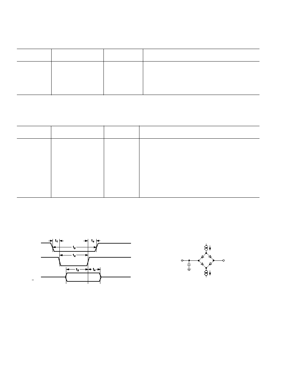
PARALLEL INTERFACE TIMING DIAGRAM
CS
WR
A4A0, CAL,
OFFS SEL
Figure 1. Parallel Write (SHA Mode Only)
I
OL
200 A
I
OH
200 A
C
L
50pF
TO
OUTPUT
PIN
1.6V
Figure 2. Load Circuit for D
OUT
Timing Specifications
AD5533
5
REV. 0
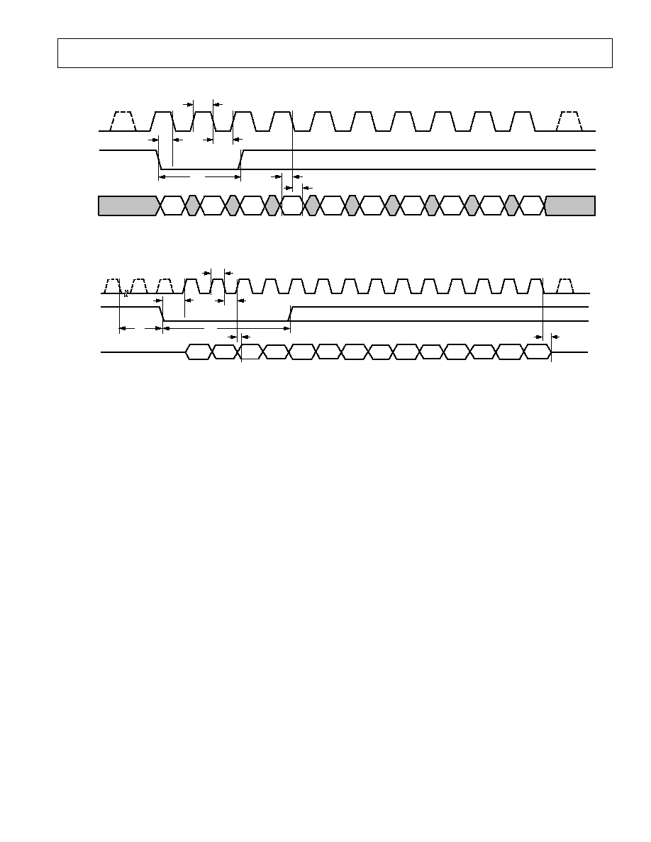
SERIAL INTERFACE TIMING DIAGRAMS
1
2
3
4
5
6
7
8
9
10
t
1
t
2
t
3
t
4
t
5
t
6
MSB
LSB
SCLK
SYNC
D
IN
Figure 3. 10-Bit Write (SHA Mode and Both Readback Modes)
t
10
2
t
1
t
2
1
3
4
5
6
7
8
9
10
11
12
13
14
t
7
t
4
t
8
t
9
MSB
LSB
SCLK
SYNC
D
OUT
10
Figure 4. 14-Bit Read (Both Readback Modes)