Äîêóìåíòàöèÿ è îïèñàíèÿ www.docs.chipfind.ru
REV. 0
Information furnished by Analog Devices is believed to be accurate and
reliable. However, no responsibility is assumed by Analog Devices for its
use, nor for any infringements of patents or other rights of third parties that
may result from its use. No license is granted by implication or otherwise
under any patent or patent rights of Analog Devices.
a
AD5532HS*
One Technology Way, P.O. Box 9106, Norwood, MA 02062-9106, U.S.A.
Tel: 781/329-4700
www.analog.com
Fax: 781/326-8703
© Analog Devices, Inc., 2001
32-Channel 14-Bit DAC with
High-Speed 3-Wire Serial Interface
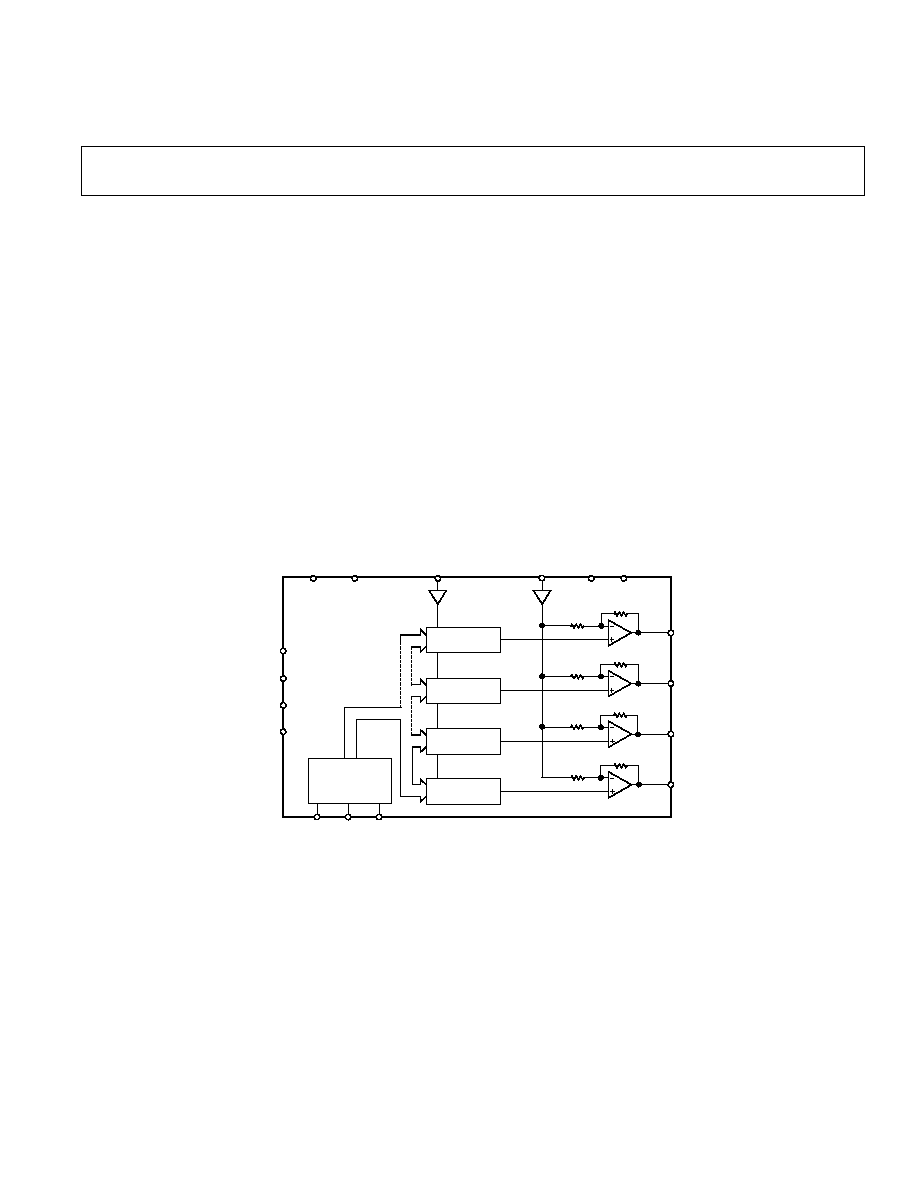
FUNCTIONAL BLOCK DIAGRAM
DAC
R
R
R
R
R
V
DD
V
SS
R
R
R
V
OUT
0
V
OUT
1
V
OUT
30
V
OUT
31
14-BIT B
U
S
RESET
DAC_GND
AGND
DGND
DV
CC
AV
CC
REF_IN
OFFS_IN
INTERFACE
CONTROL
LOGIC
AD5532HS
DAC
DAC
DAC
D
IN
SCLK
SYNC
FEATURES
High Integration: 32-Channel DAC in 12 12 mm
2
LFBGA
Guaranteed Monotonic
DSP-/Microcontroller-Compatible Serial Interface
Channel Update Rate 1.1 MHz
Output Impedance 0.5
Selectable Output Voltage 0 V to 5 V or 2.5 V to +2.5 V
Asynchronous
RESET Facility
Temperature Range 40 C to +85 C
APPLICATIONS
Optical Networks
Level Setting
Instrumentation
Automatic Test Equipment
Industrial Control Systems
Data Acquisition
Low Cost I/O
GENERAL DESCRIPTION
The AD5532HS is a 32-channel voltage-output 14-bit DAC
with a high-speed serial interface. The selected DAC register is
written to via the 3-wire interface. The serial interface operates
at clock rates up to 30 MHz and is compatible with DSP and
microcontroller interface standards. The output voltage range is
0 V to 5 V or 2.5 V to +2.5 V and is determined by the offset
voltage at the OFFS_IN pin. It is restricted to a range from
V
SS
+ 2 V to V
DD
2 V because of the headroom of the out-
put amplifier.
The device is operated with AV
CC
= 5 V
± 5%, DV
CC
= 2.7 V
to 5.25 V, V
SS
= 4.75 V to 12 V and V
DD
= +4.75 V to +12 V
and requires a stable 2.5 V reference on REF_IN.
PRODUCT HIGHLIGHTS
1. 32 14-bit DACs in one package, guaranteed monotonic.
2. The AD5532HS is available in a 74-ball LFBGA package
with a body size of 12 mm by 12 mm.
*Protected by U.S. Patent No. 5,969,657; other patents pending.

REV. 0
2
AD5532HSSPECIFICATIONS
(V
DD
= +4.75 V to +12 V, V
SS
= 4.75 V to 12 V; AV
CC
= 4.75 V to 5.25 V; DV
CC
= 2.7 V to 5.25 V; AGND = DGND = DAC_GND = 0 V; REF_IN =
2.5 V; OFFS_IN = 0 V; All outputs unloaded. All specifications T
MIN
to T
MAX
unless otherwise noted.)
A Version
2
Parameter
1
Min
Typ
Max
Unit
Conditions/Comments
D
AC DC PERFORMANCE
Resolution
14
Bits
Integral Nonlinearity (INL)
0.39
±0.1
+0.39
% of FSR
See TPC 7
Differential Nonlinearity (DNL)
1
±0.5
+1
LSB
Monotonic
Offset Error
10
+15
+50
mV
See TPC 8
Full-Scale Error
1
0.3
+0.5
% of FSR
See TPC 9
VOLTAGE REFERENCE REF_IN
Input Voltage Range
3
2.375
2.5
2.625
V
Input Current
±0.001
±1
µA
ANALOG INPUT OFFS_IN
Input Voltage Range
3, 4
0
V
DD
1.5
V
Input Current
±0.1
±1
µA
ANALOG OUTPUTS (V
OUT
0V
OUT
31)
Output Temperature Coefficient
3,
5
20
ppm/
°C
DC Output Impedance
3
0.5
Output Range
4
OFFS_IN = 0
0 2REF_IN
V
OFFS_IN = REF_IN
REF_IN to +REF_IN
V
Resistive Load
3
5
k
Capacitive Load
3
100
pF
Short-Circuit Current
3
7
mA
DC Power-Supply Rejection Ratio
3
70
dB
V
DD
= +10 V
± 5%
70
dB
V
SS
= 10 V
± 5%
DC Crosstalk
3
120
µV
DIGITAL INPUTS
3
Input Current
±5
±10
µA
Input Low Voltage
0.8
V
DV
CC
= 5 V
± 5%
0.4
V
DV
CC
= 3 V
± 10%
Input High Voltage
2.4
V
DV
CC
= 5 V
± 5%
2.0
V
DV
CC
= 3 V
± 10%
Input Hysteresis (SCLK and SYNC Only)
200
mV
Input Capacitance
10
pF
POWER SUPPLY VOLTAGES
V
DD
+4.75
+12
V
V
SS
4.75
12
V
AV
CC
4.75
5.25
V
DV
CC
2.7
5.25
V
POWER SUPPLY CURRENTS
6
I
DD
9
12
mA
All Channels Full Scale
I
SS
9
12
mA
All Channels Full Scale
AI
CC
6.5
10
mA
DI
CC
0.1
0.5
mA
V
IH
= DV
CC
and V
IL
= DGND
POWER DISSIPATION
6
123
mW
V
DD
= +5 V, V
SS
= 5 V
NOTES
1
See Terminology
2
A Version: Industrial temperature range 40
°C to +85°C; typical at 25°C.
3
Guaranteed by design and characterization, not production tested.
4
Output range is restricted from V
SS
+ 2 V to V
DD
2 V.
5
AD780 as reference for the AD5532HS.
6
Outputs unloaded.
Specifications subject to change without notice.
REV. 0
3
AD5532HS
(V
DD
= +4.75 V to +12 V, V
SS
= 4.75 V to 12 V; AV
CC
= 4.75 V to 5.25 V; DV
CC
= 2.7 V to 5.25 V; AGND =
DGND = DAC_GND = 0 V; REF_IN = 2.5 V; All outputs unloaded. All specifications T
MIN
to T
MAX
unless otherwise noted.)
Parameter
1,
2
A Version
3
Unit
Conditions/Comments
Output Voltage Settling Time
4
10
µs max
100 pF, 5 k
Load; Full-Scale Change
Slew Rate
0.85
V/
µs typ
Digital-to-Analog Glitch Impulse
1
nV-s typ
1 LSB Change around Major Carry
Digital Crosstalk
5
nV-s typ
Analog Crosstalk
1
nV-s typ
Digital Feedthrough
0.2
nV-s typ
Output Noise Spectral Density @ 1 kHz
170
nV/
Hz typ
NOTES
1
See Terminology
2
Guaranteed by design and characterization, not production tested
3
B Version: Industrial temperature range 40
°C to +85°C.
4
Timed from the end of a write sequence.
Specifications subject to change without notice.
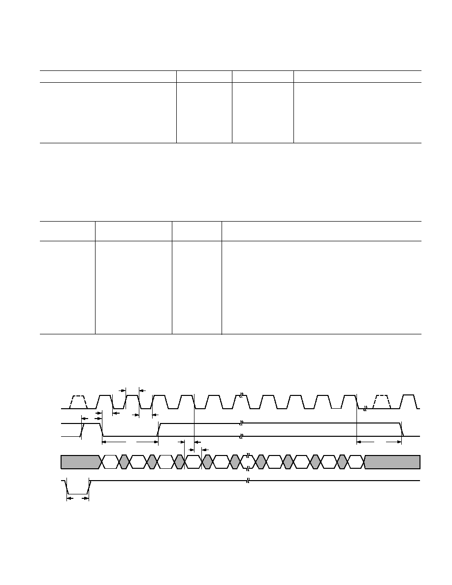
TIMING CHARACTERISTICS
Limit at T
MIN
, T
MAX
Parameter
1,
2,
3
(A Version)
Unit
Conditions/Comments
f
UPDATE
1.1
MHz max
Channel Update Rate
f
CLKIN
30
MHz max
SCLK Frequency
t
1
13
ns min
SCLK High Pulsewidth
t
2
13
ns min
SCLK Low Pulsewidth
t
3
15
ns min
SYNC Falling Edge to SCLK Falling Edge Setup Time
t
4
50
ns min
SYNC Low Time
t
5
10
ns min
SYNC High Time
t
6
10
ns min
D
IN
Setup Time
t
7
5
ns min
D
IN
Hold Time
t
8
280
ns min
19th SCLK Falling Edge to SYNC Falling Edge for Next Write
t
9
20
ns min
RESET Pulsewidth
NOTES
1
See Timing Diagrams in Figure 1.
2
Guaranteed by design and characterization, not production tested.
3
All input signals are specified with t
R
= t
F
= 5 ns (10% to 90% of DV
CC
) and timed from a voltage level of (V
IL
+ V
IH
)/2.
Specifications subject to change without notice.
AC CHARACTERISTICS
(V
DD
= +4.75 V to +12 V, V
SS
= 4.75 V to 12 V; AV
CC
= 4.75 V to 5.25 V; DV
CC
= 2.7 V to 5.25 V;
AGND = DGND = DAC_GND = 0 V; All specifications T
MIN
to T
MAX
unless otherwise noted.)
1
2
3
4
5
t
1
t
2
t
3
t
4
LSB
t
6
t
7
16
17
18
19
MSB
SCLK
SYNC
D
IN
t
8
1
t
9
RESET
t
5
Figure 1. Serial Interface Timing Diagram
REV. 0
AD5532HS
4
CAUTION
ESD (electrostatic discharge) sensitive device. Electrostatic charges as high as 4000 V readily
accumulate on the human body and test equipment and can discharge without detection. Although
the AD5532HS features proprietary ESD protection circuitry, permanent damage may occur on
devices subjected to high-energy electrostatic discharges. Therefore, proper ESD precautions are
recommended to avoid performance degradation or loss of functionality.
WARNING!
ESD SENSITIVE DEVICE
ABSOLUTE MAXIMUM RATINGS
1,
2
(T
A
= 25
°C unless otherwise noted)
V
DD
to AGND . . . . . . . . . . . . . . . . . . . . . . . . 0.3 V to +17 V
V
SS
to AGND . . . . . . . . . . . . . . . . . . . . . . . . +0.3 V to 17 V
AV
CC
to AGND, DAC_GND . . . . . . . . . . . . . 0.3 V to +7 V
DV
CC
to DGND . . . . . . . . . . . . . . . . . . . . . . . 0.3 V to +7 V
Digital Inputs to DGND . . . . . . . . . . 0.3 V to DV
CC
+ 0.3 V
REF_IN to AGND, DAC_GND . . . . . . . . . . . 0.3 V to +7 V
V
OUT
0V
OUT
31 to AGND . . . . . . . V
SS
0.3 V to V
DD
+ 0.3 V
V
OUT
0V
OUT
31 to V
SS
. . . . . . . . . . . . . . . . . . 0.3 V to +24 V
OFFS_IN to AGND . . . . . . . . . . . V
SS
0.3 V to V
DD
+ 0.3 V
AGND to DGND . . . . . . . . . . . . . . . . . . . . . 0.3 V to +0.3 V
Operating Temperature Range
Industrial . . . . . . . . . . . . . . . . . . . . . . . . . . 40
°C to +85°C
Storage Temperature Range . . . . . . . . . . . . 65
°C to +150°C
Junction Temperature (T
J
max) . . . . . . . . . . . . . . . . . . 150
°C
74-Lead LFBGA Package,
JA
Thermal Impedance . . . 41
°C/W
Reflow Soldering
Peak Temperature . . . . . . . . . . . . . . . . . . . . . . . . . . 220
°C
Time at Peak Temperature . . . . . . . . . . . . 10 sec to 40 sec
Max Power Dissipation at T
A
= 70
°C,
Outputs Loaded . . . . . . . . . . . . . . . . . . . . . . . . . . 550 mW
3
(for T
A
> 70
°C, derate at 26 mW for each °C over 70°C)
NOTES
1
Stresses above those listed under Absolute Maximum Ratings may cause perma-
nent damage to the device. This is a stress rating only; functional operation of the
device at these or any other conditions above those listed in the operational
sections of this specification is not implied. Exposure to absolute maximum rating
conditions for extended periods may affect device reliability.
2
Transient currents of up to 100 mA will not cause SCR latch-up.
3
This limit includes load power and applies only when there is a resistive load on
V
OUT
outputs.
ORDERING GUIDE
Output
Package
Package
Model
Function
Voltage Span
Description
Option
AD5532HSABC
32 DACs
5 V
74-Ball LFBGA
BC-74
OUTPUT V
O
L
T
A
GE
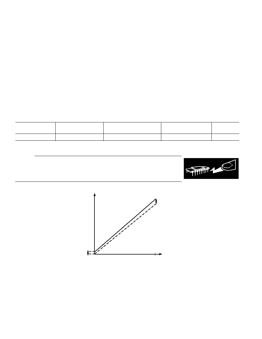
DAC CODE
FULL-SCALE
ERROR
ACTUAL
IDEAL
OFFSET
ERROR
16k
0
Figure 2. DAC Transfer Function (OFFS_IN = 0)
REV. 0
AD5532HS
5
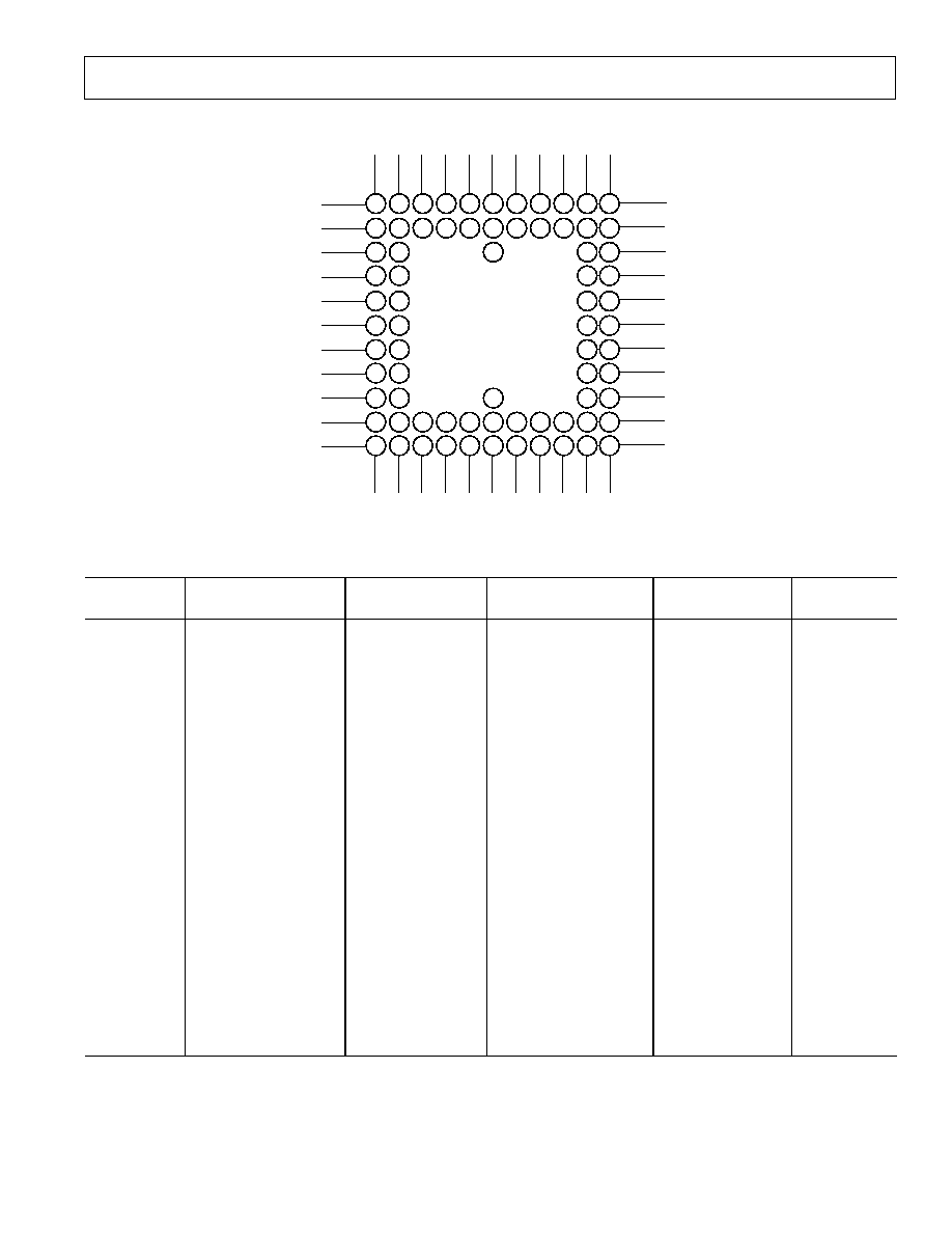
PIN CONFIGURATION
1
2
3
4
5
6
7
8
9
10
11
A
B
C
D
E
F
G
H
J
K
L
TOP VIEW
A
B
C
D
E
F
G
H
J
K
L
1
2
3
4
5
6
7
8
9
10
11
AD5532HS 74-Ball (LFBGA) Configuration
LFBGA
Ball
LFBGA
Ball
LFBGA
Ball
Number
Name
Number
Name
Number
Name
A1
N/C
C10
AVCC1
J10
VO9
A2
N/C
C11
N/C
J11
VO11
A3
N/C
D1
VO20
K1
VO17
A4
N/C
D2
DAC_GND2
K2
VO15
A5
SYNC
D10
AVCC2
K3
VO27
A6
DVCC
D11
N/C
K4
VSS3
A7
SCLK
E1
VO26
K5
VSS1
A8
N/C
E2
VO14
K6
VSS4
A9
N/C
E10
AGND1
K7
VDD2
A10
RESET
E11
OFFS_IN
K8
VO2
A11
N/C
F1
VO25
K9
VO10
B1
VO16
F2
VO21
K10
VO13
B2
N/C
F10
AGND2
K11
VO12
B3
N/C
F11
VO6
L1
N/C
B4
N/C
G1
VO24
L2
VO28
B5
N/C
G2
VO8
L3
VO29
B6
DGND
G10
VO5
L4
VO30
B7
DIN
G11
VO3
L5
VDD3
B8
DGND
H1
VO23
L6
VDD1
B9
N/C
H2
N/C
L7
VDD4
B10
N/C
H10
VO4
L8
VO31
B11
REF_IN
H11
VO7
L9
VO0
C1
VO18
J1
VO22
L10
VO1
C2
DAC_GND1
J2
VO19
L11
N/C
C6
N/C
J6
VSS2

REV. 0
AD5532HS
6
PIN FUNCTION DESCRIPTIONS
Pin
Function
AGND (12)
Analog GND Pins.
AV
CC
(12)
Analog Supply Pins. Voltage range from 4.75 V to 5.25 V.
V
DD
(14)
V
DD
Supply Pins. Voltage range from 8 V to 12 V.
V
SS
(14)
V
SS
Supply Pins. Voltage range from 4.75 V to 12 V.
DGND
Digital GND Pins.
DV
CC
Digital Supply Pins. Voltage range from 2.7 V to 5.25 V.
DAC_GND (12)
Reference GND Supply for All the DACs.
REF_IN
Reference Voltage for Channels 031.
V
OUT
0V
OUT
31
Analog Output Voltages from the 32 Channels.
SYNC
Active Low Input. This is the Frame Synchronization signal for the serial interface. While SYNC is low,
data is transferred in on the falling edge of SCLK.
SCLK
*
Serial Clock Input. Data is clocked into the shift register on the falling edge of SCLK. This
operates at clock speeds up to 30 MHz.
D
IN
*
Serial Data Input. Data must be valid on the falling edge of SCLK.
OFFS_IN
Offset Input. The user can connect this to GND or REF_IN to determine the output span.
RESET*
Active Low Input. This pin can also be used to reset the complete device to its power-on-reset conditions.
*Internal pull-up device on this logic input. Therefore, it can be left floating and will default to a logic high condition.
TERMINOLOGY
Integral Nonlinearity (INL)
A measure of the maximum deviation from a straight line pass-
ing through the endpoints of the DAC transfer function. It is
expressed as a percentage of full-scale range.
Differential Nonlinearity (DNL)
The difference between the measured change and the ideal 1 LSB
change between any two adjacent codes. A specified DNL of
±1 LSB maximum ensures monotonicity.
Offset Error
A measure of the error present at the device output with all 0s
loaded to the DAC. It includes the offset of the DAC and the
output amplifier. It is expressed in mV.
Full-Scale Error
A measure of the output error with all 1s loaded to the DAC.
Ideally the output should be 2 REF_IN if OFFS_IN = 0. It is
expressed as a percentage of full-scale range.
DC Power-Supply Rejection Ratio (PSRR)
A measure of the change in analog output for a change in supply
voltage (V
DD
and V
SS
). It is expressed in dB. V
DD
and V
SS
are
varied
±5%.
DC Crosstalk
The dc change in the output level of one DAC at midscale in
response to a full-scale code change (all 0s to all 1s and vice
versa) and output change of all other DACs. It is expressed in
µV.
Output Temperature Coefficient
A measure of the change in analog output with changes in tem-
perature. It is expressed in ppm/
°C.
Output Voltage Settling Time
The time taken from when the last data bit is clocked into the
DAC until the output has settled to within
± 0.5 LSB of its
final value.
Digital-to-Analog Glitch Impulse
The area of the glitch injected into the analog output when
the code in the DAC register changes state. It is specified as
the area of the glitch in nV-secs when the digital code is changed
by 1 LSB at the major carry transition (011 . . . 11 to 100 . . . 00
or 100 . . . 00 to 011 . . . 11).
Digital Crosstalk
The glitch impulse transferred to the output of one DAC at
midscale while a full-scale code change (all 1s to all 0s and vice
versa) is being written to another DAC. It is expressed in nV-secs.
Analog Crosstalk
The area of the glitch transferred to the output (V
OUT
) of one
DAC due to a full-scale change in the output (V
OUT
) of another
DAC. The area of the glitch is expressed in nV-secs.
Digital Feedthrough
A measure of the impulse injected into the analog outputs from the
digital control inputs when the part is not being written to, i.e.,
SYNC is high. It is specified in nV-secs and measured with a
worst-case change on the digital input pins, e.g., from all 0s
to all 1s and vice versa.
Output Noise Spectral Density
A measure of internally generated random noise. Random noise is
characterized as a spectral density (voltage per root Hertz). It is
measured by loading all DACs to midscale and measuring
noise at the output. It is measured in nV/
Hz.
REV. 0
AD5532HS
7
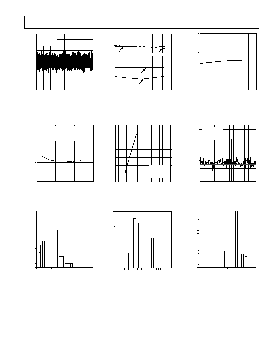
Typical Performance Characteristics
DAC CODE
D
A
C
ERR
OR LSBs
1.0
0
V
REF_IN
= 2.5V
V
OFFS_IN
= 0V
T
A
= 25 C
2K
4K
6K
8K
10K 12K 14K16K
0.8
0.6
0.4
0.2
0.0
0.2
0.4
0.6
0.8
1.0
TPC 1. Typical DNL Plot
SINK/SOURCE CURRENT mA
V
OUT
V
2.535
2.530
2.520
6
4
2
0
2.525
T
A
= 25 C
V
REFIN
= 2.5V
V
OFFS_IN
= 0V
DAC LOADED TO MIDSCALE
2
4
6
TPC 4. V
OUT
Source and Sink
Capability
% FSR
FREQ
UENCY
%
15
10
0
0
0.1
5
0.2
0.3
TPC 7. INL Error Distribution at 25
°C
DNL ERR
OR
LSBs
1.0
40
0
40
80
0.5
0.0
0.5
1.0
INL ERR
OR
% FSR
0.2
0.1
0.0
0.1
0.2
TEMPERATURE C
DNL MIN
INL MIN
INL MAX
DNL MAX
TPC 2. INL Error and DNL Error vs.
Temperature
V
OUT
V
1
1
2
3
4
5
6
0
T
A
= 25 C
V
REFIN
= 2.5V
V
OFFS_IN
= 0V
TIME BASE 1.25 s/DIV
TPC 5. Full-Scale Settling Time
mV
FREQ
UENCY
%
15
10
0
0
10
30
5
20
TPC 8. Offset Error Distribution
at 25
°C
TEMPERATURE C
V
OUT
V
5.000
4.995
4.985
40
0
40
80
4.990
V
REFIN
= 2.5V
V
OFFS_IN
= 0V
DAC LOADED TO FULL SCALE
TPC 3. V
OUT
vs. Temperature
TIME BASE 200ns/DIV
V
OUT
V
2.494
2.506
2.508
2.510
2.512
2.514
2.516
2.518
2.520
T
A
= 25 C
V
REFIN
= 2.5V
V
OFFS_IN
= 0V
2.498
2.500
2.502
2.504
2.496
TPC 6. Major Code Transition Glitch
Impulse
% FSR
FREQ
UENCY
%
20
10
0
1.0
0.5
0.0
TPC 9. Full-Scale Error Distribution
at 25
°C
REV. 0
AD5532HS
8
FUNCTIONAL DESCRIPTION
The AD5532HS consists of 32 DACs in a single package. A
14-bit digital word is loaded into one of the 32 DAC registers
via the serial interface. This is then converted (with gain and
offset) into an analog output voltage (V
OUT
0V
OUT
31).
To update a DAC's output voltage, the required DAC is
addressed via the serial port. When the 5-bit DAC address
and 14-bit DAC data have been loaded the selected DAC
converts the code.
On power-on, all the DACs are loaded with zeros.
Digital-to-Analog Section
The architecture of each DAC channel consists of a resistor-
string DAC followed by an output buffer amplifier. The voltage
at the REF_IN pin provides the reference voltage for the cor-
responding DAC. Since the input coding to the DAC is straight
binary, the ideal DAC output voltage is given by:
V
V
D
DAC
REF
IN
=
×
_
2
14
where D = decimal equivalent of the binary code that is loaded
to the DAC register i.e., 016,383.
Output Buffer Stage--Gain and Offset
The function of the output buffer stage is to translate the
0 V2.5 V output of the DAC to a wider range. This is done by
gaining up the DAC output by two and offsetting the voltage
by the voltage on OFFS_IN pin.
V
V
V
OUT
DAC
OFFS
IN
=
×
(
)
_
2
V
DAC
is the output of the DAC.
V
OFFS_IN
is the voltage at the OFFS_IN pin.
Table I shows how the output range of V
OUT
relates to the offset
voltage supplied by the user.
Table I. Sample Output Voltage Ranges
V
OFFS_IN
V
DAC
V
OUT
(V)
(V)
(V)
0
0 to 2.5
0 to 5
2.5
0 to 2.5
2.5 to +2.5
V
OUT
is limited only by the headroom of the output amplifiers.
V
OUT
must be within maximum ratings.
Reset Function
The reset function on the AD5532HS can be used to reset all
nodes on the device to their power-on-reset condition. All the
DACs are loaded with 0s and all registers are cleared. The reset
function is implemented by taking the RESET pin low.
SERIAL INTERFACE
The serial interface is controlled by three pins as follows:
SYNC: This pin is the Frame Synchronization pin for the serial
interface.
SCLK: This pin is the Serial Clock Input. It operates at clock
speeds up to 30 MHz.
D
IN
: This pin is the Serial Data Input. Data must be valid on
the falling edge of SCLK.
To update a single DAC channel a 19-bit data-word is written
into the AD5532HS. See Table II.
Table II. Serial Data Format
MSB
LSB
A4
A3
A2
A1
A0
DB13DB0
A4A0 Bits
Used to address any one of the 32 channels (A4 = MSB of
address, A0 = LSB).
DB13DB0 Bits
These are used to write a 14-bit word into the addressed
DAC register.
Figure 1 shows the timing diagram for a serial write to the
AD5532HS. The serial interface works with both a continuous and
a noncontinuous serial clock. The first falling edge of SYNC resets
a counter that counts the number of serial clocks to ensure
the correct number of bits are shifted in and out of the serial
shift registers. Any further edges on SYNC are ignored until the
correct number of bits are shifted in or out. Once 19 bits have
been shifted in or out, the SCLK is ignored. In order for another
serial transfer to take place, the counter must be reset by the
falling edge of SYNC. The user must allow 280 ns (min)
between successive writes (refer to Timing Specifications).
REV. 0
AD5532HS
9
MICROPROCESSOR INTERFACING
AD5532HS-to-ADSP-21xx Interface
The ADSP-21xx family of DSPs are easily interfaced to the
AD5532HS without the need for extra logic.
A data transfer is initiated by writing a word to the Tx register
after the SPORT has been enabled. In a write sequence, data is
clocked out on each rising edge of the DSP's serial clock and
clocked into the AD5532HS on the falling edge of its SCLK.
The easiest way to provide the 19-bit data-word required by
the AD5532HS, is to transmit two 10-bit data-words from the
ADSP-21xx. Ensure that the data is positioned correctly in the
TX register so that the first 19 bits transmitted contain valid
data. The SPORT control register should be set up as follows:
TFSW
= 1, Alternate Framing
INVTFS = 1, Active Low Frame Signal
DTYPE = 00, Right Justify Data
ISCLK
= 1, Internal Serial Clock
TFSR
= 1, Frame Every Word
ITFS
= 1, Internal Framing Signal
SLEN
= 1001, 10-Bit Data Word
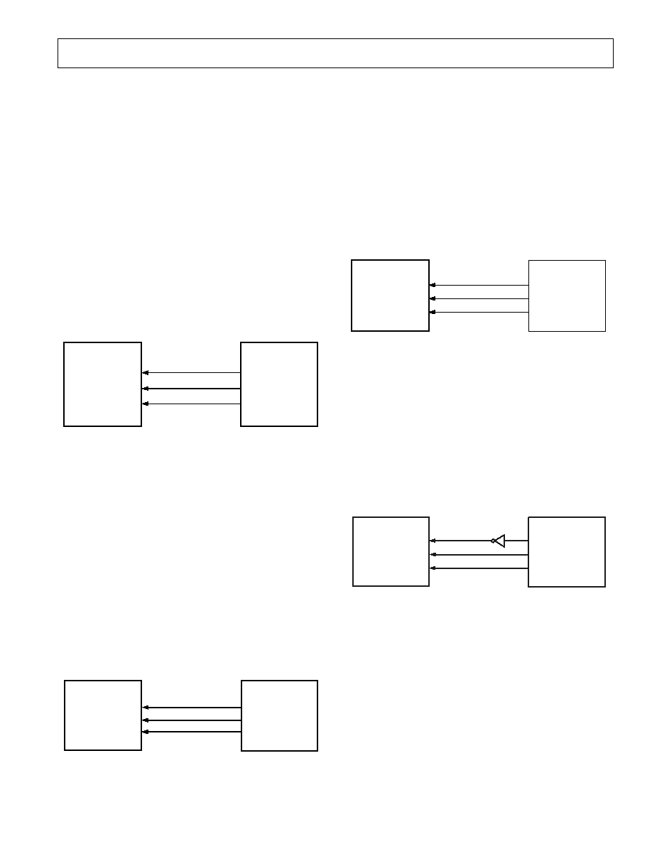
Figure 3 shows the connection diagram.
SCLK
AD5532HS*
SYNC
TFS
D
IN
DT
SCLK
ADSP-2101/
ADSP-2103*
*ADDITIONAL PINS OMITTED FOR CLARITY
Figure 3. AD5532HS-to-ADSP-2101/ADSP-2103 Interface
AD5532HS-to-MC68HC11 Interface
The Serial Peripheral Interface (SPI) on the MC68HC11 is
configured for Master Mode (MSTR = 1), Clock Polarity Bit
(CPOL) = 0 and the Clock Phase Bit (CPHA) = 1. The SPI is
configured by writing to the SPI Control Register (SPCR)--see
68HC11 User Manual. SCK of the 68HC11 drives the SCLK of
the AD5532HS and the MOSI output drives the serial data line
(D
IN
) of the AD5532HS. The SYNC signal is derived from a port
line (PC7). When data is being transmitted to the AD5532HS, the
SYNC line is taken low (PC7). Data appearing on the MOSI
output is valid on the falling edge of SCK. The 68HC11 transfers
only eight bits of data during each serial transfer operation;
therefore, three consecutive write operations are necessary to
transmit 19 bits of data. Data is transmitted MSB first. It is
important to left-justify the data in the SPDR register so that
the first 19 bits transmitted contain valid data. PC7 must be
pulled low to start a transfer. It is taken high and pulled low
again before any further write cycles can take place. See Figure 4.
SCLK
AD5532HS*
SYNC
D
IN
PC7
SCK
MC68HC11*
*ADDITIONAL PINS OMITTED FOR CLARITY
MOSI
Figure 4. AD5532HS-to-MC68HC11 Interface
AD5532HS-to-PIC16C6x/7x Interface
The PIC16C6x/7x Synchronous Serial Port (SSP) is configured
as an SPI Master with the Clock Polarity bit = 0. This is done
by writing to the Synchronous Serial Port Control Register
(SSPCON). See user PIC16/17 Microcontroller User Manual.
In this example I/O port RA1 is being used to pulse SYNC
and enable the serial port of the AD5532HS. This microcontroller
transfers only eight bits of data during each serial transfer
operation; therefore, three consecutive write operations are
necessary to transmit 19 bits of data. Data is transmitted MSB
first. It is important to left-justify the data in the SPDR register
so that the first 19 bits transmitted contain valid data. RA1
must be pulled low to start a transfer. It is taken high and pulled
low again before any further write cycles can take place. Figure 5
shows the connection diagram.
SCLK
PIC16C6x/7x*
SYNC
D
IN
SCK/RC3
AD5532HS*
*ADDITIONAL PINS OMITTED FOR CLARITY
SDI/RC4
RA1
Figure 5. AD5532HS-to-PIC16C6x/7x Interface
AD5532HS-to-8051 Interface
The AD5532HS requires a clock synchronized to the serial
data. The 8051 serial interface must therefore be operated in
Mode 0. In this mode serial data exits the 8051 through RxD
and a shift clock is output on TxD. The SYNC signal is derived
from a port line (P1.1). Figure 6 shows how the 8051 is connected
to the AD5532HS. Because the AD5532HS shifts data out on
the rising edge of the shift clock and latches data in on the
falling edge, the shift clock must be inverted. Note also that
the AD5532HS requires its data with the MSB first. Since the
8051 outputs the LSB first, the transmit routine must take this
into account.
AD5532HS*
SCLK
D
IN
SYNC
TxD
RxD
P1.1
8051*
*ADDITIONAL PINS OMITTED FOR CLARITY
Figure 6. AD5532HS-to-8051 Interface
REV. 0
AD5532HS
10
APPLICATION CIRCUITS
AD5532HS in an Optical Network Control Loop
The AD5532HS can be used in optical network applications
that require a large number of DACs to perform a control and
measurement function. In the circuit shown in Figure 7, the
0 V5 V outputs of the AD5532HS are amplified to a range of
0 V180 V and then used to control actuators that determine
the position of MEMS mirrors in an optical switch. The exact
position of each mirror is measured using sensors. The sensor
readings are muxed using four dual 4-channel matrix switches
(ADG739) and fed back to an 8-channel 14-bit ADC (AD7856).
The control loop is driven by an ADSP-21065L, a 32-bit SHARC
®
DSP with an SPI-compatible SPORT interface. It writes data
to the DAC, controls the multiplexor, and reads data from
the ADC via a 3-wire serial interface.
0V180V
AMPS
ACTUATORS
FOR MEMS
MIRROR
ARRAY
AD7856
ADSP-21065L
S
E
N
S
O
R
S
1
32
1
32
1
8
ADG739
4
AD5532HS
Figure 7. AD5532HS and DSP Control an Optical Switch
Alternatively, the AD5532HS can be driven by an ADMC401
Motor-Controller as shown in the control-loop in Figure 8. The
DAC outputs are fed into eight AD8534 quad transconductance
amps to generate currents for voice-coil actuators that determine
the position of the mirrors. The exact position of each mirror
is measured and the readings are muxed into the on-chip
8-channel ADC of the ADMC401.
1
32
AD5532HS
AD8534
8
ADMC401
S
E
N
S
O
R
S
1
8
ADG704
8
S
P
O
R
T
3
AD8544
2
3
8-CH
12-BIT
ADC
1
8
1
32
VOICE-COIL
ACTUATORS
FOR
MEMS
MIRROR
ARRAY
Figure 8. AD5532HS and ADMC401 Control an Optical
Switch
AD5532HS in a Typical ATE System
The AD5532HS is ideally suited for use in Automatic Test
Equipment. Several DACs are required to control pin drivers,
comparators, active loads, and signal timing. Traditionally,
sample-and-hold devices were used in this application.
The AD5532HS has several advantages: no refreshing is required,
there is no droop, pedestal error is eliminated, and there is no
need for extra filtering to remove glitches. A higher level of
integration is achieved in a smaller area (see Figure 9).
DACs
ACTIVE
LOAD
DRIVER
COMPARATOR
FORMATTER
COMPARE
REGISTER
STORED
DATA
AND INHIBIT
PATTERN
PERIOD
GENERATION
AND
DELAY
TIMING
SYSTEM BUS
SYSTEM BUS
DUT
DAC
DAC
DAC
DAC
DAC
DAC
DAC
PARAMETRIC
MEASUREMENT
UNIT
Figure 9. AD5532HS in an ATE System
POWER SUPPLY DECOUPLING
In any circuit where accuracy is important, careful consideration
of the power supply and ground return layout helps to ensure
the rated performance. The printed circuit board on which the
AD5532HS is mounted should be designed so that the analog
and digital sections are separated, and confined to certain areas
of the board. If the AD5532HS is in a system where multiple
devices require an AGND-to-DGND connection, the connection
should be made at one point only. The star ground point should
be established as close as possible to the device. For supplies
with multiple pins (V
SS
, V
DD
, AV
CC
), it is recommended to
tie those pins together. The AD5532HS should have ample
supply bypassing of 10
µF in parallel with 0.1 µF on each supply
located as close to the package as possible, ideally right up against
the device. The 10
µF capacitors are the tantalum bead type. The
0.1
µF capacitor should have low Effective Series Resistance
(ESR) and Effective Series Inductance (ESI), like the common
ceramic types that provide a low impedance path to ground at
high frequencies, to handle transient currents due to internal
logic switching.
The power supply lines of the AD5532HS should use as large a
trace as possible to provide low impedance paths and reduce
the effects of glitches on the power supply line. Fast switching
signals such as clocks should be shielded with digital ground to
avoid radiating noise to other parts of the board, and should
never be run near the reference inputs. A ground line routed
between the D
IN
and SCLK lines will help reduce crosstalk
between them (not required on a multilayer board as there will
be a separate ground plane, but separating the lines will help). It
is essential to minimize noise on REF_IN.
Avoid crossover of digital and analog signals. Traces on opposite
sides of the board should run at right angles to each other. This
reduces the effects of feedthrough through the board. A microstrip
technique is by far the best, but not always possible with a double-
sided board. In this technique, the component side of the board
is dedicated to ground plane while signal traces are placed on
the solder side.
As is the case for all thin packages, care must be taken to avoid
flexing the package and to avoid a point load on the surface of
the package during the assembly process.
SHARC is a registered trademark of Analog Devices, Inc.
REV. 0
AD5532HS
11
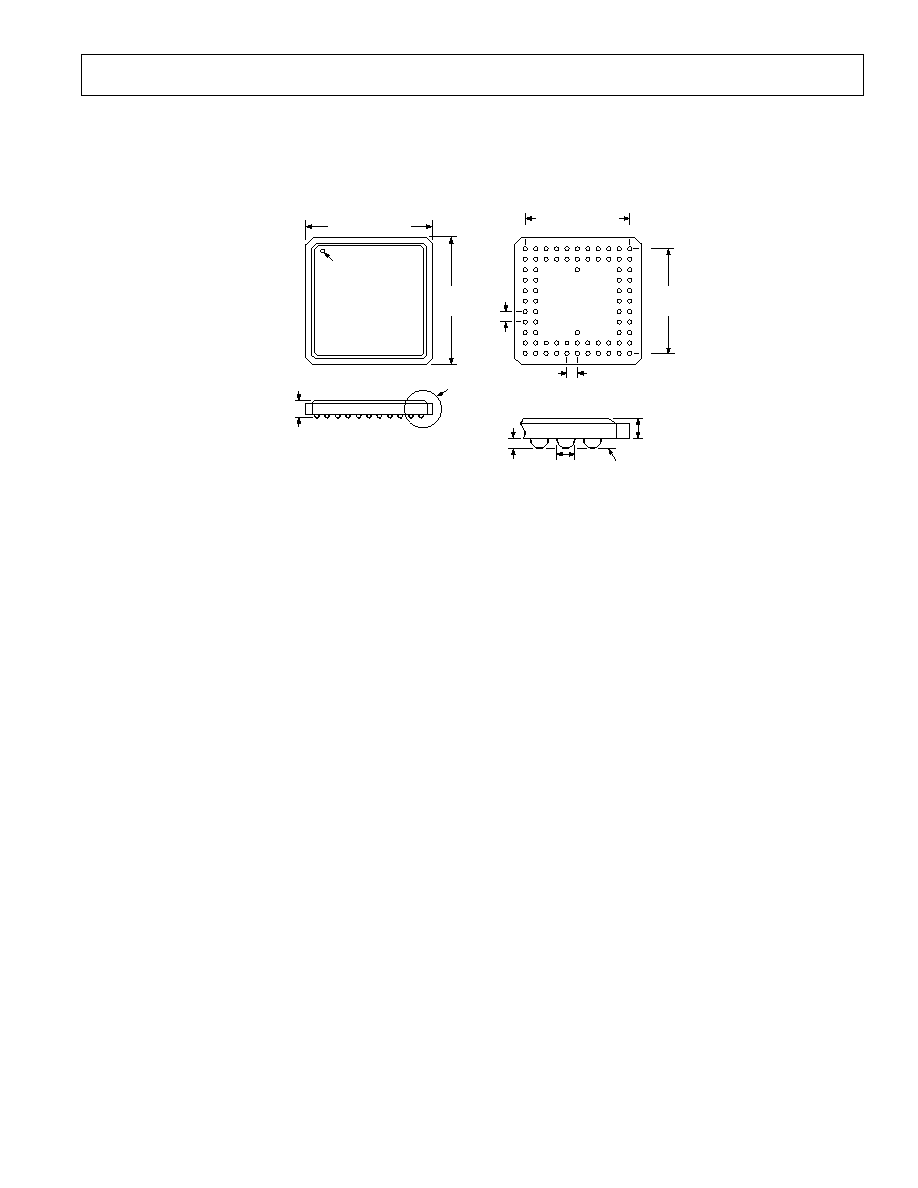
74-Ball LFBGA
(BC-74)
A
B
C
D
E
F
G
H
J
K
L
11 10 9 8 7 6 5 4 3 2 1
0.039
(1.00)
BSC
0.039 (1.00) BSC
BOTTOM
VIEW
0.394
(10.00)
BSC
0.394 (10.00) BSC
A1
TOP VIEW
0.472 (12.00) BSC
0.472
(12.00)
BSC
DETAIL A
0.067
(1.70)
MAX
SEATING
PLANE
DETAIL A
0.024 (0.60)
BSC
BALL DIAMETER
0.033
(0.85)
MIN
0.020
(0.50)
MIN
CONTROLLING DIMENSIONS
ARE IN MILLIMETERS
OUTLINE DIMENSIONS
Dimensions shown in inches and (mm).

12
PRINTED IN U.S.A.
C02548
1.5
6/01(0)
Document Outline
- Specifications
- Pinout
- Package Drawings
- Ordering Guide
- Features
- Applications
- Product Description
- Timing characteristics
- Absolute Maximum Ratings
- Functional Block Diagram
- Pin Function Description
- PRODUCT HIGHLIGHTS
- CAUTION
- SERIAL INTERFACE
- DIN:
- APPLICATION CIRCUITS
- POWER SUPPLY DECOUPLING
- DIAGRAMS
- Serial Interface Timing Diagram
- AD5532HS-to-ADSP-2101/ADSP-2103 Interface
- AD5532HS-to-MC68HC11 Interface
- AD5532HS-to-PIC16C6x/7x Interface
- AD5532HS-to-8051 Interface
- AD5532HS and DSP Control an Optical Switch
- AD5532HS and ADMC401 Control an Optical Switch
- AD5532HS in an ATE System