 | ÐлекÑÑоннÑй компоненÑ: AD5552 | СкаÑаÑÑ:  PDF PDF  ZIP ZIP |
Äîêóìåíòàöèÿ è îïèñàíèÿ www.docs.chipfind.ru
REV. 0
Information furnished by Analog Devices is believed to be accurate and
reliable. However, no responsibility is assumed by Analog Devices for its
use, nor for any infringements of patents or other rights of third parties
which may result from its use. No license is granted by implication or
otherwise under any patent or patent rights of Analog Devices.
a
AD5551/AD5552
One Technology Way, P.O. Box 9106, Norwood, MA 02062-9106, U.S.A.
Tel: 781/329-4700
World Wide Web Site: http://www.analog.com
Fax: 781/326-8703
© Analog Devices, Inc., 2000
5 V, Serial-Input
Voltage-Output, 14-Bit DACs
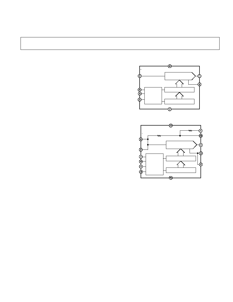
FUNCTIONAL BLOCK DIAGRAMS
SERIAL
INPUT
REGISTER
V
REF
CS
DIN
SCLK
AGND
V
OUT
V
DD
DGND
AD5551
14-BIT
DAC
14-BIT
DATA
LATCH
CONTROL
LOGIC
SERIAL
INPUT
REGISTER
V
REFF
CS
DIN
SCLK
AGNDF
V
OUT
V
DD
DGND
AD5552
14-BIT
DAC
14-BIT
DATA
LATCH
CONTROL
LOGIC
V
REFS
LDAC
AGNDS
RFB
INV
R
FB
R
INV
FEATURES
Full 14-Bit Performance
5 V Single Supply Operation
Low Power
Fast Settling Time
Unbuffered Voltage Output Capable of Driving 60 k
Loads Directly
SPITM/QSPITM/MICROWIRETM-Compatible Interface
Standards
Power-On Reset Clears DAC Output to 0 V (Unipolar
Mode)
Schmitt Trigger Inputs for Direct Optocoupler Interface
APPLICATIONS
Digital Gain and Offset Adjustment
Automatic Test Equipment
Data Acquisition Systems
Industrial Process Control
GENERAL DESCRIPTION
The AD5551 and AD5552 are single, 14-bit, serial input, voltage
output DACs that operate from a single 5 V
± 10% supply.
The AD5551 and AD5552 utilize a versatile 3-wire interface that
is compatible with SPI, QSPI, MICROWIRE, and DSP inter-
face standards.
These DACs provide 14-bit performance without any adjust-
ments. The DAC output is unbuffered, which reduces power
consumption and offset errors contributed by an output buffer.
With an external op amp the AD5552 can be operated in bipo-
lar mode generating a
±V
REF
output swing. The AD5552 also
includes Kelvin sense connections for the reference and analog
ground pins to reduce layout sensitivity. For higher precision
applications, please refer to 16-bit DACs AD5541, AD5542,
and AD5544.
The AD5551 and AD5552 are available in an SO package.
PRODUCT HIGHLIGHTS
1. Single Supply Operation.
The AD5551 and AD5552 are fully specified and guaranteed
for a single 5 V
± 10% supply.
2. Low Power Consumption.
Typically 1.5 mW with a 5 V supply.
3. 3-Wire Serial Interface.
4. Unbuffered output capable of driving 60 k
loads, which
reduces power consumption as there is no internal buffer
to drive.
5. Power-On Reset Circuitry.
SPI and QSPI are trademarks of Motorola, Inc.
MICROWIRE is a trademark of National Semiconductor Corporation.

2
REV. 0
AD5551/AD5552SPECIFICATIONS
Parameter
Min
Typ
Max
Unit
Test Condition
STATIC PERFORMANCE
Resolution
14
Bits
Relative Accuracy, INL
±0.15
±1.0
LSB
B Grade
Differential Nonlinearity
±0.15
±0.8
LSB
Guaranteed Monotonic
Gain Error
1.75 0.3
0
LSB
Gain Error Temperature Coefficient
±0.1
ppm/
°C
Zero Code Error
0
0.1
0.5
LSB
Zero Code Temperature Coefficient
±0.05
ppm/
°C
AD5552
Bipolar Resistor Matching
1.000
/
R
FB
/R
INV
, Typically R
FB
= R
INV
= 28 k
±0.0015 ±0.0152
%
Ratio Error
Bipolar Zero Offset Error
±0.25
±2.5
LSB
Bipolar Zero Temperature Coefficient
±0.2
ppm/
°C
OUTPUT CHARACTERISTICS
Output Voltage Range
0
V
REF
1 LSB
V
Unipolar Operation
V
REF
V
REF
1 LSB
V
AD5552 Bipolar Operation
Output Voltage Settling Time
1
µs
to 1/2 LSB of FS, C
L
= 10 pF
Slew Rate
25
V/
µs
C
L
= 10 pF, Measured from 0% to 63%
Digital-to-Analog Glitch Impulse
10
nV-s
1 LSB Change Around the Major Carry
Digital Feedthrough
10
nV-s
All 1s Loaded to DAC, V
REF
= 2.5 V
DAC Output Impedance
6.25
k
Tolerance Typically 20%
Power Supply Rejection Ratio
±1.0
LSB
V
DD
± 10%
DAC REFERENCE INPUT
Reference Input Range
2.0
V
DD
V
Reference Input Resistance
2
9
k
Unipolar Operation
7.5
k
AD5552, Bipolar Operation
LOGIC INPUTS
Input Current
±1
µA
V
INL
, Input Low Voltage
0.8
V
V
INH
, Input High Voltage
2.4
V
Input Capacitance
3
10
pF
Hysteresis Voltage
3
0.4
V
REFERENCE
Reference 3 dB Bandwidth
1.3
MHz
All 1s Loaded
Reference Feedthrough
1
mV p-p
All 0s Loaded, V
REF
= 1 V p-p at 100 kHz
Signal-to-Noise Ratio
92
dB
Reference Input Capacitance
75
pF
Code 0000
H
120
pF
Code 3FFF
H
POWER REQUIREMENTS
V
DD
4.50
5.50
V
I
DD
0.3
1.1
mA
Power Dissipation
1.5
6.05
mW
NOTES
1
Temperature range is as follows: B Version: 40
°C to +85°C.
2
Reference input resistance is code-dependent, minimum at 2555
H
.
3
Guaranteed by design, not subject to production test.
Specifications subject to change without notice.
(V
DD
= 5 V 10%, V
REF
= 2.5 V, AGND = DGND = 0 V. All specifications
T
A
= T
MIN
to T
MAX
,
unless otherwise noted.)
AD5551/AD5552
3
REV. 0
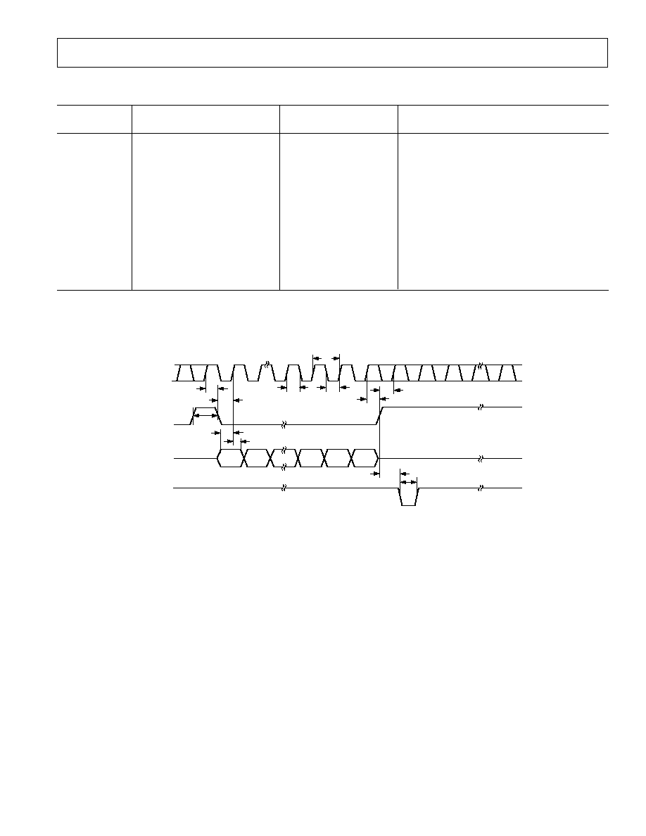
SCLK
CS
DIN
DB13
LDAC
*
DB0
t
1
*
AD5552
ONLY. MAY BE TIED PERMANENTLY LOW IF REQUIRED.
t
2
t
3
t
5
t
6
t
7
t
8
t
9
t
11
t
4
t
10
t
12
Figure 1. Timing Diagram
TIMING CHARACTERISTICS
1,
2
Limit at T
MIN
, T
MAX
Parameter
All Versions
Unit
Description
f
SCLK
25
MHz max
SCLK Cycle Frequency
t
1
40
ns min
SCLK Cycle Time
t
2
20
ns min
SCLK High Time
t
3
20
ns min
SCLK Low Time
t
4
15
ns min
CS Low to SCLK High Setup
t
5
15
ns min
CS High to SCLK High Setup
t
6
35
ns min
SCLK High to
CS Low Hold Time
t
7
20
ns min
SCLK High to
CS High Hold Time
t
8
15
ns min
Data Setup Time
t
9
0
ns min
Data Hold Time
t
10
30
ns min
LDAC Pulsewidth
t
11
30
ns min
CS High to LDAC Low Setup
t
12
30
ns min
CS High Time Between Active Periods
NOTES
1
Guaranteed by design. Not production tested.
2
Sample tested during initial release and after any redesign or process change that may affect this parameter. All input signals are measured with tr = tf = 5 ns (10% to
90% of +3 V and timed from a voltage level of +1.6 V).
Specifications subject to change without notice.
(V
DD
= 5 V 5%, V
REF
= 2.5 V, AGND = DGND = 0 V. All specifications T
A
= T
MIN
to T
MAX
,
unless
otherwise noted.)
AD5551/AD5552
4
REV. 0
CAUTION
ESD (electrostatic discharge) sensitive device. Electrostatic charges as high as 4000 V readily
accumulate on the human body and test equipment and can discharge without detection. Although
the AD5551/AD5552 features proprietary ESD protection circuitry, permanent damage may occur
on devices subjected to high-energy electrostatic discharges. Therefore, proper ESD precautions
are recommended to avoid performance degradation or loss of functionality.
WARNING!
ESD SENSITIVE DEVICE
ABSOLUTE MAXIMUM RATINGS
*
(T
A
= 25
°C unless otherwise noted)
V
DD
to AGND . . . . . . . . . . . . . . . . . . . . . . . . . 0.3 V to +6 V
Digital Input Voltage to DGND . . . . . 0.3 V to V
DD
+ 0.3 V
V
OUT
to AGND . . . . . . . . . . . . . . . . . . 0.3 V to V
DD
+ 0.3 V
AGND, AGNDF, AGNDS to DGND . . . . . 0.3 V to +0.3 V
Input Current to Any Pin Except Supplies . . . . . . . .
±10 mA
Operating Temperature Range
Industrial (B Version) . . . . . . . . . . . . . . . . 40
°C to +85°C
Storage Temperature Range . . . . . . . . . . . . 65
°C to +150°C
Maximum Junction Temperature, (T
J
max) . . . . . . . . . 150
°C
ORDERING GUIDE
Model
INL
DNL
Temperature Range
Package Description
Package Option
AD5551BR
±1 LSB
±0.8 LSB
40
°C to +85°C
8-Lead Small Outline IC
SO-8
AD5552BR
±1 LSB
±0.8 LSB
40
°C to +85°C
14-Lead Small Outline IC
R-14
Die Size = 80 139 = 11,120 sq mil; Number of Transistors = 1230.
Package Power Dissipation . . . . . . . . . . . . . (T
J
max T
A
)/
JA
Thermal Impedance
JA
SOIC (SO-8) . . . . . . . . . . . . . . . . . . . . . . . . . . 149.5
°C/W
SOIC (R-14) . . . . . . . . . . . . . . . . . . . . . . . . . . 104.5
°C/W
Lead Temperature, Soldering
Vapor Phase (60 sec) . . . . . . . . . . . . . . . . . . . . . . . . 215
°C
Infrared (15 sec) . . . . . . . . . . . . . . . . . . . . . . . . . . . . 220
°C
*Stresses above those listed under Absolute Maximum Ratings may cause perma-
nent damage to the device. This is a stress rating only; functional operation of the
device at these or any other conditions above those listed in the operational
sections of this specification is not implied. Exposure to absolute maximum rating
conditions for extended periods may affect device reliability.
AD5551 PIN FUNCTION DESCRIPTIONS
Mnemonic
Pin No.
Description
V
OUT
1
Analog Output Voltage from the DAC.
AGND
2
Ground Reference Point for Analog Circuitry.
V
REF
3
This is the voltage reference input for the DAC. Connect to external reference ranges from
2 V to V
DD
.
CS
4
This is an active low-logic input signal. The chip select signal is used to frame the serial
data input.
SCLK
5
Clock Input. Data is clocked into the input register on the rising edge of SCLK. Duty cycle
must be between 40% and 60%.
DIN
6
Serial Data Input. This device accepts 14-bit words. Data is clocked into the input register on
the rising edge of SCLK.
DGND
7
Digital Ground. Ground reference for digital circuitry.
V
DD
8
Analog Supply Voltage, 5 V
± 10%.
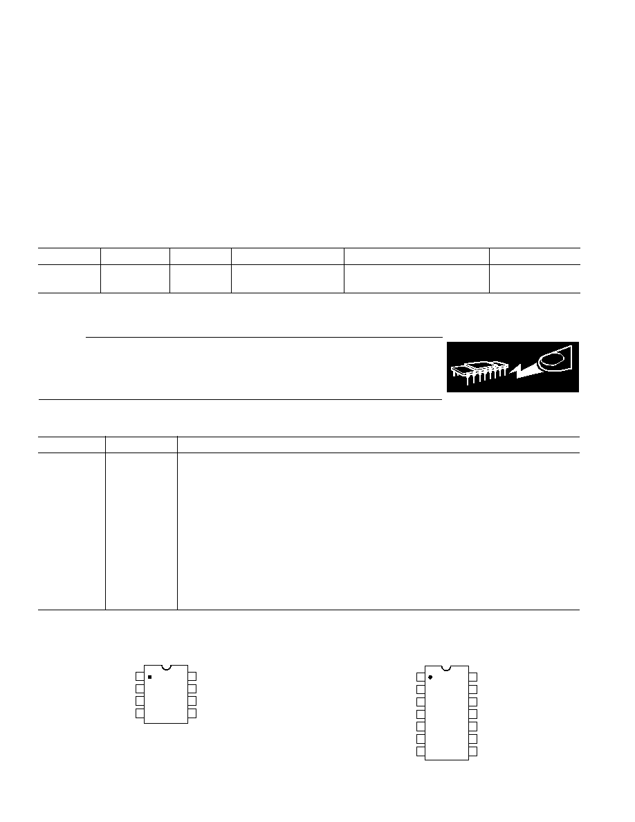
AD5551 PIN CONFIGURATION
SOIC
TOP VIEW
(Not to Scale)
8
7
6
5
1
2
3
4
V
OUT
AGND
V
REF
V
DD
DGND
DIN
SCLK
CS
AD5551
AD5552 PIN CONFIGURATION
SOIC
TOP VIEW
(Not to Scale)
14
13
12
11
10
9
8
1
2
3
4
5
6
7
NC = NO CONNECT
RFB
V
OUT
AGNDF
AGNDS
V
REFS
V
REFF
CS
V
DD
INV
DGND
LDAC
DIN
NC
SCLK
AD5552

AD5551/AD5552
5
REV. 0
AD5552 PIN FUNCTION DESCRIPTIONS
Mnemonic
Pin No.
Description
RFB
1
Feedback Resistor. In bipolar mode connect this pin to external op amp output.
V
OUT
2
Analog Output Voltage from the DAC.
AGNDF
3
Ground Reference Point for Analog Circuitry (Force).
AGNDS
4
Ground Reference Point for Analog Circuitry (Sense).
V
REFS
5
This is the voltage reference input (sense) for the DAC. Connect to external reference ranges from
2 V to V
DD
.
V
REFF
6
This is the voltage reference input (force) for the DAC. Connect to external reference ranges
from 2 V to V
DD
.
CS
7
This is an active low-logic input signal. The chip select signal is used to frame the serial data input.
SCLK
8
Clock input. Data is clocked into the input register on the rising edge of SCLK. Duty cycle
must be between 40% and 60%.
NC
9
No Connect.
DIN
10
Serial Data Input. This device accepts 14-bit words. Data is clocked into the input register on
the rising edge of SCLK.
LDAC
11
LDAC Input. When this input is taken low, the DAC register is simultaneously updated with
the contents of the input register.
DGND
12
Digital Ground. Ground reference for digital circuitry.
INV
13
Connected to the Internal Scaling Resistors of the DAC. Connect INV pin to external op amps
inverting input in bipolar mode.
V
DD
14
Analog Supply Voltage, 5 V
± 10%.
TERMINOLOGY
Relative Accuracy
For the DAC, relative accuracy or integral nonlinearity (INL)
is a measure of the maximum deviation, in LSBs, from a straight
line passing through the endpoints of the DAC transfer function.
A typical INL versus code plot can be seen in TPC 1.
Differential Nonlinearity
Differential nonlinearity is the difference between the measured
change and the ideal 1 LSB change between any two adjacent
codes. A specified differential nonlinearity of
±1 LSB maximum
ensures monotonicity. TPC 4 illustrates a typical DNL versus
code plot.
Gain Error
Gain error is the difference between the actual and ideal analog
output range, expressed as a percent of the full-scale range.
It is the deviation in slope of the DAC transfer characteristic
from ideal.
Gain Error Temperature Coefficient
This is a measure of the change in gain error with changes in
temperature. It is expressed in ppm/
°C.
Zero Code Error
Zero code error is a measure of the output error when zero code
is loaded to the DAC register.
Zero Code Temperature Coefficient
This is a measure of the change in zero code error with a change
in temperature. It is expressed in mV/
°C.
Digital-to-Analog Glitch Impulse
Digital-to-analog glitch impulse is the impulse injected into the
analog output when the input code in the DAC register changes
state. It is normally specified as the area of the glitch in nV-s
and is measured when the digital input code is changed by 1 LSB
at the major carry transition. A plot of the glitch impulse is shown
in TPC 14.
Digital Feedthrough
Digital feedthrough is a measure of the impulse injected into the
analog output of the DAC from the digital inputs of the DAC,
but is measured when the DAC output is not updated.
CS is
held high, while the CLK and DIN signals are toggled. It is
specified in nV-s and is measured with a full-scale code change
on the data bus, i.e., from all 0s to all 1s and vice versa. A typi-
cal plot of digital feedthrough is shown in TPC 13.
Power Supply Rejection Ratio
This specification indicates how the output of the DAC is affected
by changes in the power supply voltage. Power-supply rejection
ratio is quoted in terms of % change in output per % change in
V
DD
for full-scale output of the DAC. V
DD
is varied by
±10%.
Reference Feedthrough
This is a measure of the feedthrough from the V
REF
input to the
DAC output when the DAC is loaded with all 0s. A 100 kHz,
1 V p-p is applied to V
REF
. Reference feedthrough is expressed
in mV p-p.