 | ÐлекÑÑоннÑй компоненÑ: AD5553CRM | СкаÑаÑÑ:  PDF PDF  ZIP ZIP |
Äîêóìåíòàöèÿ è îïèñàíèÿ www.docs.chipfind.ru
a
AD5543/AD5553
Current Output/
Serial Input, 16-/14-Bit DAC
REV. A
Information furnished by Analog Devices is believed to be accurate and
reliable. However, no responsibility is assumed by Analog Devices for its
use, nor for any infringements of patents or other rights of third parties that
may result from its use. No license is granted by implication or otherwise
under any patent or patent rights of Analog Devices. Trademarks and
registered trademarks are the property of their respective companies.
One Technology Way, P.O. Box 9106, Norwood, MA 02062-9106, U.S.A.
Tel: 781/329-4700
www.analog.com
Fax: 781/326-8703
© 2003 Analog Devices, Inc. All rights reserved.
FEATURES
16-Bit Resolution AD5543
14-Bit Resolution AD5553
1 LSB DNL
2 LSB INL for AD5543
1 LSB INL for AD5553
Low Noise 12 nV/
Hz
Low Power, I
DD
= 10 A
0.5 s Settling Time
4Q Multiplying Reference-Input
2 mA Full-Scale Current
20%, with V
REF
= 10 V
Built-in RFB Facilitates Voltage Conversion
3-Wire Interface
Ultracompact MSOP-8 and SOIC-8 Packages
APPLICATIONS
Automatic Test Equipment
Instrumentation
Digitally Controlled Calibration
Industrial Control PLCs
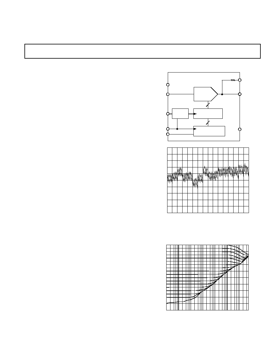
FUNCTIONAL BLOCK DIAGRAM
16-/14-BIT SHIFT
REGISTER
DAC
REGISTER
AD5543/AD5553
D/A
CONVERTER
V
DD
V
REF
R
FB
I
OUT
CS
CLK
SDI
GND
16 OR 14
16 OR 14
CONTROL
LOGIC
CODE
1.0
4096
INL LSB
0.8
8152
12288
16384
20480
24575
28672
32768
36864
40960
45056
49152
53248
57344
61440
65536
0.6
0.4
0.2
0
0.2
0.4
0.6
0.8
1.0
0
Figure 1. Integral Nonlinearity Error
FFFFH
START 10.000Hz
1k
100k
10
100
10k
1M
10M
8000H
4000H
1000H
0800H
0400H
0200H
0100H
0080H
0040H
0020H
0010H
0008H
0004H
0002H
0001H
0000H
STOP 50 000 000.000Hz
2000H
REF LEVEL
0.000dB
/DIV
12.000dB
MARKER 4 311 677.200Hz
MAG (A/R)
2.939dB
Figure 2. Reference Multiplying Bandwidth
GENERAL DESCRIPTION
The AD5543/AD5553 are precision 16-/14-bit, low power,
current output, small form factor digital-to-analog converters.
They are designed to operate from a single 5 V supply with a
±10 V multiplying reference.
The applied external reference V
REF
determines the full-scale
output current. An internal feedback resistor (R
FB
) facilitates the
R-2R and temperature tracking for voltage conversion when
combined with an external op amp.
A serial-data interface offers high speed, 3-wire microcontroller
compatible inputs using serial data in (SDI), clock (CLK), and
chip select (
CS).
The AD5543/AD5553 are packaged in ultracompact
(3 mm
4.7 mm) MSOP-8 and SOIC-8 packages.

REV. A
2
AD5543/AD5553SPECIFICATIONS
(@ V
DD
= 5 V 10%, V
SS
= 0 V, I
OUT
= Virtual GND, GND = 0 V, V
REF
= 10 V,
T
A
= Full operating temperature range, unless otherwise noted.)
ELECTRICAL CHARACTERISTICS
Parameter
Symbol
Condition
5 V
10% Unit
STATIC PERFORMANCE
1
Resolution
N
1 LSB = V
REF
/2
16
= 153
µV when V
REF
= 10 V AD5543
16
Bits
1 LSB = V
REF
/2
14
= 610
µV when V
REF
= 10 V AD5553
14
Bits
Relative Accuracy
INL
Grade: AD5553C
±1
LSB max
Grade: AD5543B
±2
LSB max
Differential Nonlinearity
DNL
Monotonic
±1
LSB max
Output Leakage Current
I
OUT
Data = 0000
H
, T
A
= 25
°C
10
nA max
Data = 0000
H
, T
A
= T
A
max
20
nA max
Full-Scale Gain Error
G
FSE
Data = FFFF
H
±1/±4
mV typ/max
Full-Scale Tempco
2
TCV
FS
1
ppm/
°C typ
REFERENCE INPUT
V
REF
Range
V
REF
15/+15
V min/max
Input Resistance
R
REF
5
k
typ
3
Input Capacitance
2
C
REF
5
pF typ
ANALOG OUTPUT
Output Current
I
OUT
Data = FFFF
H
for AD5543
2
mA typ
Data = 3FFF
H
for AD5553
Output Capacitance
2
C
OUT
Code Dependent
200
pF typ
LOGIC INPUTS AND OUTPUT
Logic Input Low Voltage
V
IL
0.8
V max
Logic Input High Voltage
V
IH
2.4
V min
Input Leakage Current
I
IL
10
µA max
Input Capacitance
2
C
IL
10
pF max
INTERFACE TIMING
2, 4
Clock Input Frequency
f
CLK
50
MHz
Clock Width High
t
CH
10
ns min
Clock Width Low
t
CL
10
ns min
CS to Clock Setup
t
CSS
0
ns min
Clock to
CS Hold
t
CSH
10
ns min
Data Setup
t
DS
5
ns min
Data Hold
t
DH
10
ns min
SUPPLY CHARACTERISTICS
Power Supply Range
V
DD
RANGE
4.5/5.5
V min/max
Positive Supply Current
I
DD
Logic Inputs = 0 V
10
µA max
Power Dissipation
P
DISS
Logic Inputs = 0 V
0.055
mW max
Power Supply Sensitivity
P
SS
V
DD
=
±5%
0.006
%/% max
AC CHARACTERISTICS
4
Output Voltage Settling Time
t
S
To
±0.1% of Full Scale,
0.5
µs typ
Data = 0000
H
to FFFF
H
to 0000
H
for AD5543
Data = 0000
H
to 3FFF
H
to 0000
H
for AD5553
Reference Multiplying BW
BW
V
REF
= 5 V p-p, Data = FFFF
H
4
MHz typ
DAC Glitch Impulse
Q
V
REF
= 0 V, Data = 7FFF
H
to 8000
H
for AD5543
7
nV-s typ
Data = 1FFF
H
to 2000
H
for AD5553
Feedthrough Error
V
OUT
/V
REF
Data = 0000
H
, V
REF
= 100 mV rms, same channel
65
dB
Digital Feedthrough
Q
CS = 1, and f
CLK
= 1 MHz
7
nV-s typ
Total Harmonic Distortion
THD
V
REF
= 5 V p-p, Data = FFFF
H
, f = 1 kHz
85
dB typ
Output Spot Noise Voltage
e
N
f = 1 kHz, BW = 1 Hz
12
nV/
Hz
NOTES
1
All static performance tests (except I
OUT
) are performed in a closed-loop system using an external precision OP177 I-to-V converter amplifier. The AD5543 R
FB
terminal
is tied to the amplifier output. The op amp +IN is grounded and the DAC I
OUT
is tied to the op amp IN. Typical values represent average readings measured at 25
°C.
2
These parameters are guaranteed by design and are not subject to production testing.
3
All ac characteristic tests are performed in a closed-loop system using an AD841 I-to-V converter amplifier.
4
All input control signals are specified with t
R
= t
F
= 2.5 ns (10% to 90% of 3 V) and timed from a voltage level of 1.5 V.

REV. A
AD5543/AD5553
3
ABSOLUTE MAXIMUM RATINGS
*
V
DD
to GND . . . . . . . . . . . . . . . . . . . . . . . . . . . . 0.3 V, +8 V
V
REF
to GND . . . . . . . . . . . . . . . . . . . . . . . . . . . . 18 V, +18 V
Logic Inputs to GND . . . . . . . . . . . . . . . . . . . . . 0.3 V, +8 V
V(I
OUT
) to GND . . . . . . . . . . . . . . . . . . . 0.3 V, V
DD
+ 0.3 V
Input Current to Any Pin except Supplies . . . . . . . . . .
±50 mA
Package Power Dissipation . . . . . . . . . . . . . (T
J
Max T
A
)/
JA
Thermal Resistance
JA
8-Lead Surface Mount (MSOP-8) . . . . . . . . . . . . . 150
°C/W
8-Lead Surface Mount (SOIC-8) . . . . . . . . . . . . . . 100
°C/W
Maximum Junction Temperature (T
J
Max) . . . . . . . . . . 150
°C
Operating Temperature Range
Models B, C . . . . . . . . . . . . . . . . . . . . . . . . . 40
°C to +85°C
Storage Temperature Range . . . . . . . . . . . . . 65
°C to +150°C
Lead Temperature
RN-8, RM-8 (Vapor Phase, 60 sec) . . . . . . . . . . . . . . 215
°C
RN-8, RM-8 (Infrared, 15 sec) . . . . . . . . . . . . . . . . . 220
°C
*Stresses above those listed under Absolute Maximum Ratings may cause perma-
nent damage to the device. This is a stress rating only; functional operation of the
device at these or any other conditions above those indicated in the operational
sections of this specification is not implied. Exposure to absolute maximum rating
conditions for extended periods may affect device reliability.
PIN CONFIGURATION
MSOP and SOIC-8
TOP VIEW
(Not to Scale)
8
7
6
5
1
2
3
4
CLK
AD5543/
AD5553
SDI
R
FB
V
REF
CS
GND
I
OUT
V
DD
PIN FUNCTION DESCRIPTIONS
Pin
No.
Mnemonic Function
1
CLK
Clock Input. Positive-edge triggered, clocks
data into shift register.
2
SDI
Serial Register Input. Data loads directly
into the shift register MSB first. Extra leading
bits are ignored.
3
R
FB
Internal Matching Feedback Resistor. Con-
nects to external op amp for voltage output.
4
V
REF
DAC Reference Input Pin. Establishes DAC
full-scale voltage. Constant input resistance
versus code.
5
I
OUT
DAC Current Output. Connects to inverting
terminal of external precision I-to-V op amp
for voltage output.
6
GND
Analog and Digital Ground
7
V
DD
Positive Power Supply Input. Specified range
of operation 5 V
± 10%.
8
CS
Chip Select. Active low digital input. Transfers
shift-register data to DAC register on rising
edge. See Truth Table for operation.
ORDERING GUIDE
*
INL
RES
Temperature
Package
Package
Model
(LSB)
(LSB)
Range
Description
Option
Marking
AD5543BR
±2
16
40
°C to +85°C SOIC-8
RN-8
AD5543
AD5543BRM
±2
16
40
°C to +85°C MSOP-8
RM-8
DXB
AD5553CRM
±1
14
40
°C to +85°C MSOP-8
RM-8
DUC
*The AD5543 contains 1040 transistors. The die size measures 55 mil 73 mil, 4,015 sq. mil.
CAUTION
ESD (electrostatic discharge) sensitive device. Electrostatic charges as high as 4000 V readily
accumulate on the human body and test equipment and can discharge without detection. Although the
AD5543/AD5553 features proprietary ESD protection circuitry, permanent damage may occur on
devices subjected to high energy electrostatic discharges. Therefore, proper ESD precautions are
recommended to avoid performance degradation or loss of functionality.
REV. A
4
AD5543/AD5553Typical Performance Characteristics
CODE Decimal
1.0
0
65536
8192
INL LSB
16384
24576
32768
40960
49152
57344
0.8
0.6
0.4
0.2
0
0.2
0.4
0.6
0.8
1.0
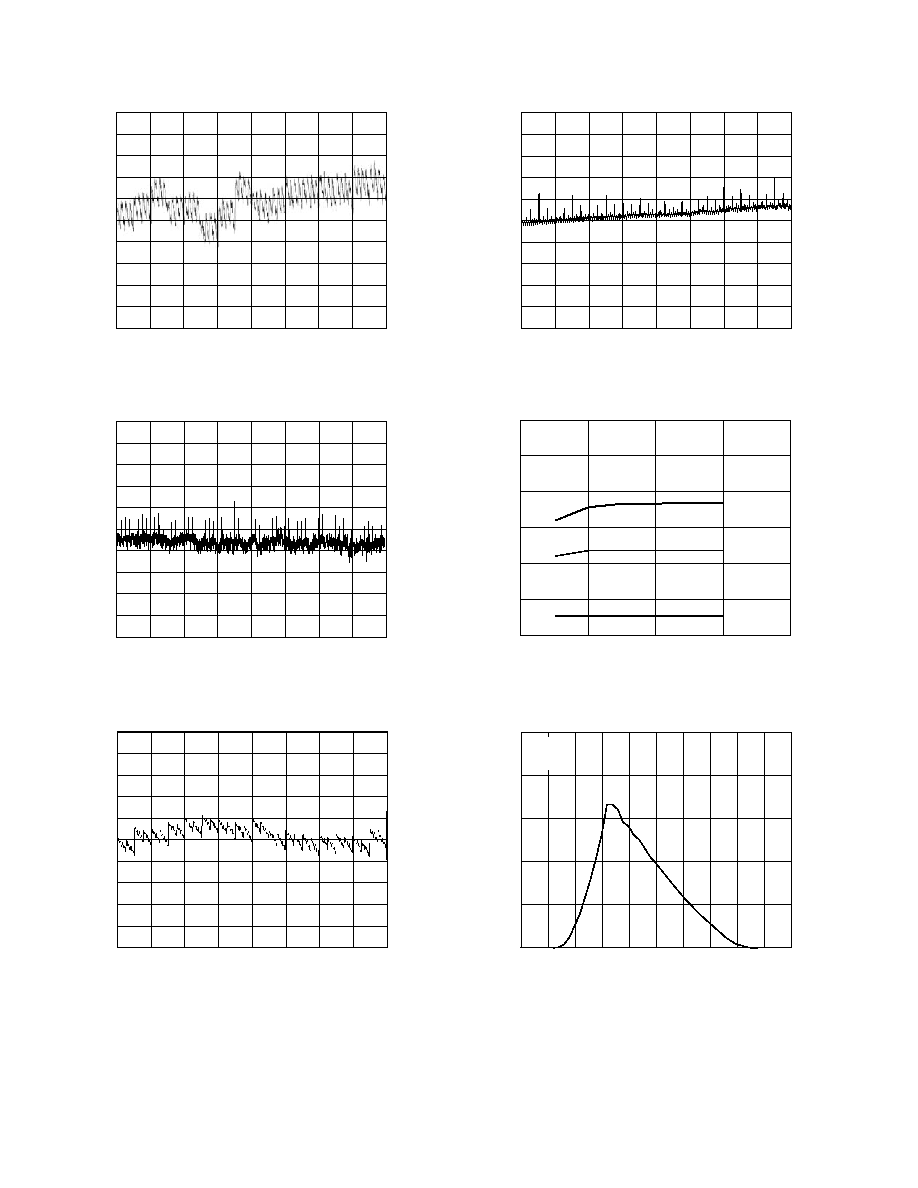
TPC 1. AD5543 Integral Nonlinearity Error
CODE Decimal
1.0
0
65536
8192
DNL LSB
16384
24576
32768
40960
49152
57344
0.8
0.6
0.4
0.2
0
0.2
0.4
0.6
0.8
1.0
TPC 2. AD5543 Differential Nonlinearity Error
CODE Decimal
1.0
0
14336
INL LSB
16384
0.8
0.6
0.4
0.2
0
0.2
0.4
0.6
0.8
1.0
12288
10240
8192
6144
4096
2048
TPC 3. AD5553 Integral Nonlinearity Error
DNL LSB
CODE Decimal
0
2048
4096
6144
8192
10240
12288
14336 16384
1.0
0.8
0.6
0.4
0.2
0
0.2
0.4
0.6
0.8
1.0
TPC 4. AD5553 Differential Nonlinearity Error
SUPPLY VOLTAGE V
DD
V
1.5
1.0
1.5
2
10
4
LINEARITY ERR
OR LSB
6
8
0.5
0
0.5
1.0
V
REF
= 2.5V
T
A
= 25 C
INL
DNL
GE
TPC 5. Linearity Errors vs. V
DD
LOGIC INPUT VOLTAGE V
IH
V
5
4
0
0.5
SUPPL
Y CURRENT I
DD
mA
3
2
1
0
V
DD
= 5V
T
A
= 25 C
1.0
2.0
1.5
2.5
3.0
3.5
4.0
4.5
5.0
TPC 6. Supply Current vs. Logic Input Voltage
REV. A
AD5543/AD5553
5
CLOCK FREQUENCY Hz
3.0
2.5
0
10k
100M
100k
SUPPL
Y CURRENT mA
1M
10M
2.0
1.5
1.0
0.5
5555
H
8000
H
FFFF
H
0000
H
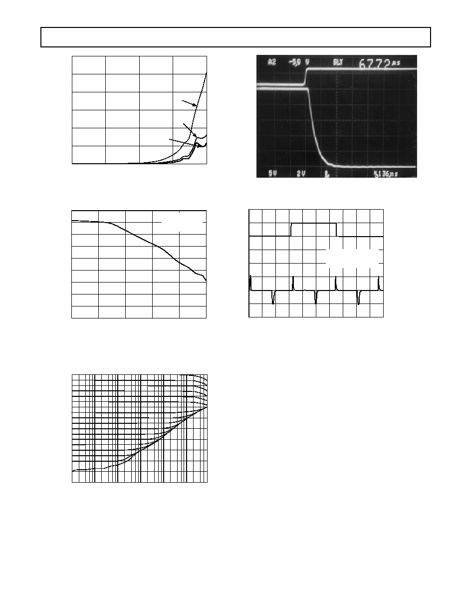
TPC 7. AD5543 Supply Current vs. Clock Frequency
FREQUENCY Hz
90
80
30
10k
100k
PSRR dB
1M
70
60
50
40
20
10
0
1k
100
10
V
DD
= 5V
10%
V
REF
= 10V
TPC 8. Power Supply Rejection vs. Frequency
FFFFH
START 10.000Hz
1k
100k
10
100
10k
1M
10M
8000H
4000H
1000H
0800H
0400H
0200H
0100H
0080H
0040H
0020H
0010H
0008H
0004H
0002H
0001H
0000H
STOP 50 000 000.000Hz
2000H
REF LEVEL
0.000dB
/DIV
12.000dB
MARKER 4 311 677.200Hz
MAG (A/R)
2.939dB
TPC 9. Reference Multiplying Bandwidth
TPC 10. Settling Time
V
OUT
(50mV/DIV)
CS (5V/DIV)
TIME s
0
0.5
1.0
1.5
2.0
2.5
3.0
3.5
4.0
4.5
5.0
V
DD
= 5V
V
REF
= 10V
CODES 8000
H
7FFF
H
TPC 11. Midscale Transition and Digital Feedthrough
REV. A
6
AD5543/AD5553
SDI
CLK
CS
t
DS
DH
t
CH
t
CL
t
t
CSH
t
CSS
D15
D14
D13
D12
D11
D10
D9
D8
D1
D0
Figure 3a. AD5543 Timing Diagram
SDI
CLK
CS
t
DS
DH
t
CH
t
CL
t
t
CSH
t
CSS
D13
D12
D11
D10
D9
D8
D1
D0
D7
D6
Figure 3b. AD5553 Timing Diagram
Table I. Control-Logic Truth Table
CLK
CS
Serial Shift Register Function
DAC Register
X
H
No Effect
Latched
+
L
Shift Register Data Advanced One Bit
Latched
X
H
No Effect
Latched
X
+
Shift Register Data Transferred to DAC Register
New Data Loaded from Serial Register
+ positive logic transition; X Don't Care
Table II. AD5543 Serial Input Register Data Format; Data is Loaded in the MSB-First Format
MSB
LSB
Bit Position
B15
B14
B13
B12
B11
B10
B9
B8
B7
B6
B5
B4
B3
B2
B1
B0
Data-Word
D15
D14
D13
D12
D11
D10
D9
D8
D7
D6
D5
D4
D3
D2
D1
D0
Table III. AD5553 Serial Input Register Data Format; Data is Loaded in the MSB-First Format
MSB
LSB
Bit Position
B13
B12
B11
B10
B9
B8
B7
B6
B5
B4
B3
B2
B1
B0
Data-Word
*
D13
D12
D11
D10
D9
D8
D7
D6
D5
D4
D3
D2
D1
D0
*A full 16-bit data-word can be loaded into the AD5553 serial input register, but only the last 14 bits entered will be transferred to the DAC register when CS returns
to logic high.
REV. A
AD5543/AD5553
7
CIRCUIT OPERATION
The AD5543/AD5553 contains a 16-/14-bit, current output,
digital-to-analog converter, a serial input register, and a DAC
register. Both converters use a 3-wire serial data interface.
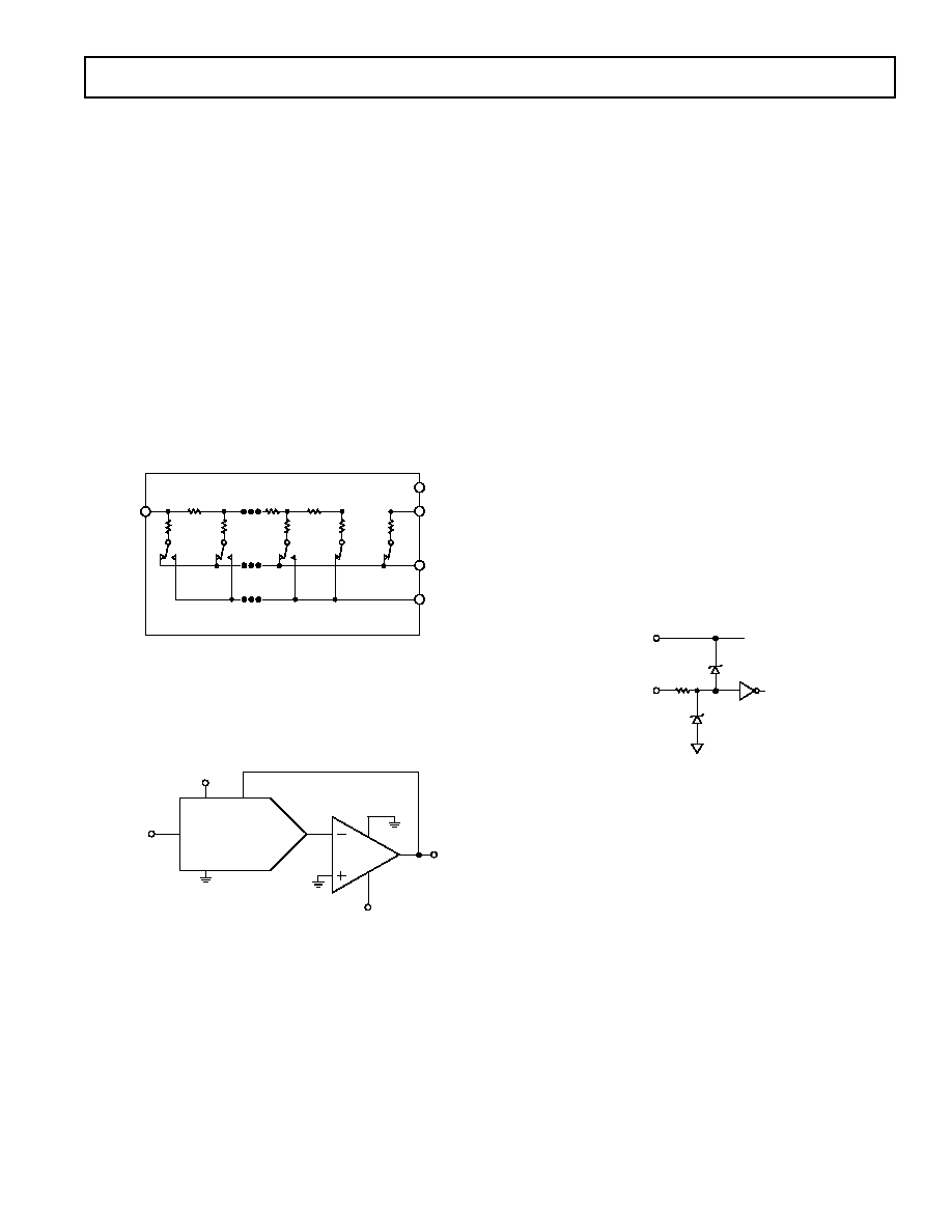
D/A Converter Section
The DAC architecture uses a current steering R-2R ladder
design. Figure 4 shows the typical equivalent DAC structure.
The DAC contains a matching feedback resistor for use with an
external op amp, (see Figure 5). With R
FB
and I
OUT
terminals
connected to the op amp output and inverting node respec-
tively, a precision voltage output can be achieved as:
V
V
D
AD
OUT
REF
=
×
/
,
(
)
65 536
5543
(1)
V
V
D
AD
OUT
REF
=
×
/
,
(
)
16 384
5553
(2)
Note that the output voltage polarity is opposite to the V
REF
polarity for dc reference voltages.
These DACs are designed to operate with either negative or
positive reference voltages. The V
DD
power pin is only used by
the internal logic to drive the DAC switches' ON and OFF states.
V
REF
V
DD
R
FB
I
OUT
R
R
R
GND
2R
2R
2R
R
5k
S1
S2
DIGITAL INTERFACE CONNECTIONS OMITTED FOR CLARITY;
SWITCHES S1 AND S2 ARE CLOSED, V
DD
MUST BE POWERED
Figure 4. Equivalent R-2R DAC Circuit
Note that a matching switch is used in series with the internal 5 k
feedback resistor. If users attempt to measure RFB, power must be
applied to V
DD
to achieve continuity.
V
DD
V
REF
V
REF
V
DD
U2
U1
AD5543/AD5553
5V
V
O
GND
I
OUT
V+
V
R
FB
AD8628
Figure 5. Voltage Output Configuration
These DACs are also designed to accommodate ac reference
input signals. The AD5543 accommodates input reference
voltages in the range of 12 V to +12 V. The reference voltage
inputs exhibit a constant nominal input resistance value of 5 k
,
±30%. The DAC output (I
OUT
) is code-dependent, producing
various resistances and capacitances. External amplifier choice
should take into account the variation in impedance generated
by the AD5543 on the amplifier's inverting input node. The
feedback resistance, in parallel with the DAC ladder resistance,
dominates output voltage noise. To maintain good analog perfor-
mance, power supply bypassing of 0.01
µF to 0.1 µF ceramic or
chip capacitors in parallel with a 1
µF tantalum capacitor is recom-
mended. Due to degradation of power supply rejection ratio in
frequency, users must avoid using switching power supplies.
SERIAL DATA INTERFACE
The AD5543/AD5553 uses a 3-wire (
CS, SDI, CLK) serial
data interface. New serial data is clocked into the serial input
register in a 16-bit data-word format for AD5543. The MSB is
loaded first. Table II defines the 16 data-word bits. Data is
placed on the SDI pin and clocked into the register on the positive
clock edge of CLK, subject to the data setup and hold time
requirements specified in the interface timing specifications.
Only the last 16 bits clocked into the serial register are inter-
rogated when the
CS pin is strobed to transfer the serial register
data to the DAC register. Since most microcontrollers output
serial data in 8-bit bytes, two data bytes can be written to the
AD5543/AD5553. After loading the serial register, the rising edge
of
CS transfers the serial register data to the DAC register;
during this strobe, the CLK should not be toggled. For the
AD5553, with 16-bit clock cycles, the two LSBs are ignored.
ESD Protection Circuits
All logic-input pins contain back-biased ESD protection Zener
diodes connected to ground (GND) and V
DD
as shown in Figure 6.
V
DD
DIGITAL
INPUTS
5k
DGND
Figure 6. Equivalent ESD Protection Circuits
PCB Layout and Power Supply Bypassing
It is a good practice to employ compact, minimum lead length
PCB layout design. The leads to the input should be as short as
possible to minimize IR drop and stray inductance.
It is also essential to bypass the power supplies with quality
capacitors for optimum stability. Supply leads to the device should
be bypassed with 0.01
µF to 0.1 µF disc or chip ceramic capaci-
tors. Low-ESR 1
µF to 10 µF tantalum or electrolytic capacitors
should also be applied at the supplies to minimize transient
disturbance and filter out low frequency ripple
The PCB metal traces between V
REF
and R
FB
should also be
matched to minimize gain error.
REV. A
8
AD5543/AD5553
APPLICATIONS
Stability
V
DD
V
REF
V
REF
V
DD
U2
U1
AD5543/AD5553
V
O
GND
I
OUT
R
FB
AD8628
C1
Figure 7. Optional Compensation Capacitor for Gain
Peaking Prevention
In the I-to-V configuration, the I
OUT
of the DAC and the inverting
node of the op amp must be connected as close as possible, and
proper PCB layout technique must be employed. Since every code
change corresponds to a step function, gain peaking may occur
if the op amp has limited GBP and there is excessive parasitic
capacitance at the inverting node.
An optional compensation capacitor C1 can be added for stability
as shown in Figure 7. C1 should be found empirically but 20 pF
is generally adequate for the compensation.
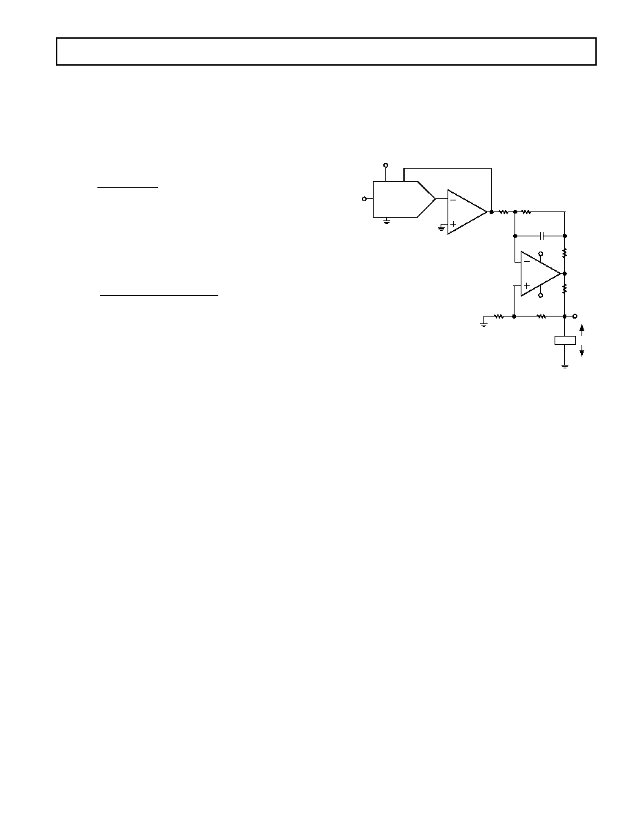
Positive Voltage Output
To achieve the positive voltage output, an applied negative
reference to the input of the DAC is preferred over the output
inversion through an inverting amplifier because of the resistor's
tolerance errors. To generate a negative reference, the reference
can be level-shifted by an op amp such that the V
OUT
and GND
pins of the reference become the virtual ground and 2.5 V
respectively, (see Figure 8).
V
REF
V
DD
U2
U1
AD5543/AD5553
V
O
GND
I
OUT
R
FB
1/2AD8628
1/2AD8620
V
OUT
V
IN
GND
V+
V
+5V
5V
ADR03
+5V
2.5V
U3
U4
C1
0 < V
O
< +2.5
Figure 8. Positive Voltage Output Configuration
Bipolar Output
The AD5543/AD5553 is inherently a 2-quadrant multiplying
D/A converter. That is, it can easily be set up for unipolar output
operation. The full-scale output polarity is the inverse of the
reference input voltage.
In some applications, it may be necessary to generate the full
4-quadrant multiplying capability or a bipolar output swing. This
is easily accomplished by using an additional external amplifier
U4 configured as a summing amplifier (see Figure 9). In this
circuit, the second amplifier U4 provides a gain of 2 that increases
the output span magnitude to 5 V. Biasing the external amplifier
with a 2.5 V offset from the reference voltage results in a full
4-quadrant multiplying circuit. The transfer equation of this circuit
shows that both negative and positive output voltages are created
as the input data (D) is incremented from code zero (V
OUT
=
2.5 V) to midscale (V
OUT
= 0 V) to full-scale (V
OUT
= +2.5 V).
V
D
V
AD
OUT
REF
=
×
(
/
,
)
(
)
32 768 1
5543
(3)
V
D
V
AD
OUT
REF
=
×
(
/
,
)
(
)
16 384
1
5553
(4)
For AD5543, the resistance tolerance becomes the dominant
error of which users should be aware.
V
REF
V
DD
U2
U1
AD5553 ONLY
V
O
GND
I
OUT
R
FB
1/2AD8620
V
OUT
V
IN
GND
ADR03
U3
1/2AD8620
V+
V
+5V
5V
+5V
U4
C1
2.5 < V
O
< +2.5
C2
5k
0.01%
R3
R1
R2
10k
0.01% 10k
0.01%
+5V
Figure 9. Four-Quadrant Multiplying Application Circuit
REV. A
AD5543/AD5553
9
Programmable Current Source
Figure 10 shows a versatile V-I conversion circuit using an
improved Howland Current Pump. In addition to the precision
current conversion it provides, this circuit enables a bidirec-
tional current flow and high voltage compliance. This circuit
can be used in 4 to 20 mA current transmitters with up to 500
of load. In Figure 10, it can be shown that if the resistor network is
matched, the load current is:
I
R
R
R
R
V
D
L
REF
=
+
(
)
×
×
2
3
1
3
/
(5)
R3 in theory can be made small to achieve the current needed
within the U3 output current driving capability. This circuit is
versatile such that AD8510 can deliver
±20 mA in both direc-
tions and the voltage compliance approaches 15 V, which is
limited mainly by the supply voltages of U3. However, users
must pay attention to the compensation. Without C1, it can be
shown that the output impedance becomes:
Z
R R R
R
R R
R
R
R
R
O
=
+
(
)
+
(
)
+
(
)
1
3
1
2
1
2
3
1
2
3
'
'
'
'
(6)
If the resistors are perfectly matched, Z
O
is infinite, which is
desirable, and behaves as an ideal current source. On the other
hand, if they are not matched, Z
O
can be either positive or nega-
tive. Negative can cause oscillation. As a result, C1 is needed to
prevent the oscillation. For critical applications, C1 could be
found empirically, but typically falls in the range of few pF.
V
REF
V
DD
U2
U1
AD5543/AD5553
V
L
GND
I
OUT
R
FB
AD8628
AD8510
V+
V
V
REF
LOAD
U3
V
DD
V
SS
R3
50
I
L
V
DD
C1
10pF
R3'
50
R2
15k
R1
150k
R2'
15k
R1'
150k
Figure 10. Programmable Current Source with Bidirec-
tional Current Control and High Voltage Compliance
Capabilities
REV. A
10
AD5543/AD5553
OUTLINE DIMENSIONS
8-Lead microSOIC Package [MSOP]
(RM-8)
Dimensions shown in millimeters
0.23
0.08
0.80
0.40
8
0
8
5
4
1
4.90
BSC
PIN 1
0.65 BSC
3.00
BSC
SEATING
PLANE
0.15
0.00
0.38
0.22
1.10 MAX
3.00
BSC
COMPLIANT TO JEDEC STANDARDS MO-187AA
COPLANARITY
0.10
8-Lead Standard Small Outline Package [SOIC]
Narrow Body
(RN-8)
Dimensions shown in millimeters and (inches)
0.25 (0.0098)
0.19 (0.0075)
1.27 (0.0500)
0.41 (0.0160)
0.50 (0.0196)
0.25 (0.0099)
45
8
0
1.75 (0.0688)
1.35 (0.0532)
SEATING
PLANE
0.25 (0.0098)
0.10 (0.0040)
8
5
4
1
5.00 (0.1968)
4.80 (0.1890)
4.00 (0.1574)
3.80 (0.1497)
1.27 (0.0500)
BSC
6.20 (0.2440)
5.80 (0.2284)
0.51 (0.0201)
0.33 (0.0130)
COPLANARITY
0.10
CONTROLLING DIMENSIONS ARE IN MILLIMETERS; INCH DIMENSIONS
(IN PARENTHESES) ARE ROUNDED-OFF MILLIMETER EQUIVALENTS FOR
REFERENCE ONLY AND ARE NOT APPROPRIATE FOR USE IN DESIGN
COMPLIANT TO JEDEC STANDARDS MS-012AA

REV. A
AD5543/AD5553
11
Revision History
Location
Page
2/03--Data Sheet changed from REV. 0 to REV. A.
Changes to ORDERING GUIDE . . . . . . . . . . . . . . . . . . . . . . . . . . . . . . . . . . . . . . . . . . . . . . . . . . . . . . . . . . . . . . . . . . . . . . . . . . . 3

C029170
2
/03(A)
PRINTED IN U.S.A.
12
Document Outline
- FEATURES
- APPLICATIONS
- GENERAL DESCRIPTION
- FUNCTIONAL BLOCK DIAGRAM
- SPECIFICATIONS
- ABSOLUTE MAXIMUM RATINGS
- ORDERING GUIDE
- PIN CONFIGURATION
- PIN FUNCTION DESCRIPTIONS
- Typical Performance Characteristics
- CIRCUIT OPERATION
- SERIAL DATA INTERFACE
- ESD Protection Circuits
- PCB Layout and Power Supply Bypassing
- APPLICATIONS
- Stability
- Positive Voltage Output
- Bipolar Output
- Programmable Current Source
- OUTLINE DIMENSIONS
- Revision History