 | ÐлекÑÑоннÑй компоненÑ: AD5641AKS | СкаÑаÑÑ:  PDF PDF  ZIP ZIP |
Äîêóìåíòàöèÿ è îïèñàíèÿ www.docs.chipfind.ru
2.7 V to 5.5 V, <100 µA, 14-Bit
nanoDACTM D/A in SC70 Package
Preliminary Technical Data
AD5641
Rev. PrC
Information furnished by Analog Devices is believed to be accurate and reliable.
However, no responsibility is assumed by Analog Devices for its use, nor for any
infringements of patents or other rights of third parties that may result from its use.
Specifications subject to change without notice. No license is granted by implication
or otherwise under any patent or patent rights of Analog Devices. Trademarks and
registered trademarks are the property of their respective owners.
One Technology Way, P.O. Box 9106, Norwood, MA 02062-9106, U.S.A.
Tel: 781.329.4700
www.analog.com
Fax: 781.326.8703
© 2004 Analog Devices, Inc. All rights reserved.
FEATURES
6-lead SC70 package
Power-down to <100 nA @ 3 V
Single 14-bit DAC:
B Version: ±4 LSB INL
A Version: ±8 LSB INL
Micropower operation: max 100 µA @ 5 V
2.7 V to 5.5 V power supply
Guaranteed monotonic by design
Power-on reset to 0 V with brownout detection
3 power-down functions
Low power serial interface with Schmitt-triggered inputs
On-chip output buffer amplifier, rail-to-rail operation
SYNC interrupt facility
APPLICATIONS
Voltage level setting
Portable battery-powered instruments
Digital gain and offset adjustment
Programmable voltage and current sources
Programmable attenuators
GENERAL DESCRIPTION
The AD5641, a member of the nanoDAC family, is a single,
14-bit, buffered, voltage out DAC that operates from a single
2.7 V to 5.5 V supply, consuming <100 µA at 5 V. The part
comes in a tiny SC70 package. Its on-chip precision output
amplifier allows rail-to-rail output swing to be achieved. The
AD5641 utilizes a versatile 3-wire serial interface that operates
at clock rates up to 30 MHz and is compatible with SPI®, QSPITM,
MICROWIRETM, and DSP interface standards. The reference for
AD5641 is derived from the power supply inputs and, therefore,
gives the widest dynamic output range. The part incorporates a
power-on reset circuit, which ensures that the DAC output
powers up to 0 V and remains there until a valid write to the
device takes place.
The AD5641 contains a power-down feature that reduces
current consumption to <100 nA at 3 V, and provides software-
selectable output loads while in power-down mode. The part is
put into power-down mode over the serial interface. The low
power consumption of the part in normal operation makes it
ideally suited to portable battery-operated equipment. The
combination of small package and low power makes this
nanoDAC device ideal for level-setting requirements such as
generating bias or control voltages in space-constrained and
power-sensitive applications.
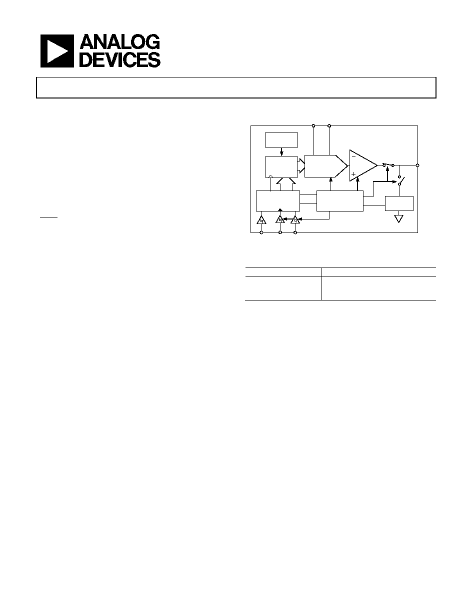
FUNCTIONAL BLOCK DIAGRAM
POWER-ON
RESET
DAC
REGISTER
14-BIT
DAC
INPUT
CONTROL
LOGIC
POWER-DOWN
CONTROL LOGIC
AD5641
V
DD
GND
REF(+)
RESISTOR
NETWORK
V
OUT
SYNC
SCLK
DIN
OUTPUT
BUFFER
04611-A
-
001
Figure 1.
Table 1. Related Devices
Part Number
Description
AD5601/AD5611/AD5621
2.7 V to 5.5 V, <100 µA, 8-/10-/12-Bit,
nanoDACTM D/A, SPI Interface, SC70
Package
The AD5641 is designed with new technology and comes in a
space-saving SC70 package.
PRODUCT HIGHLIGHTS
1.
Available in a space-saving 6-lead SC70 package.
2.
Low power, single-supply operation. The AD5641 operates
from a single 2.7 V to 5.5 V supply and typically consumes
0.2 mW at 3 V and 0.5 mW at 5 V, making it ideal for
battery-powered applications.
3.
The on-chip output buffer amplifier allows the output of
the DAC to swing rail-to-rail with a typical slew rate of
0.5 V/µs.
4.
Reference derived from the power supply.
5.
High speed serial interface with clock speeds up to
30 MHz.
6.
Designed for very low power consumption. The interface
powers up only during a write cycle.
7.
Power-down capability. When powered down, the DAC
typically consumes <100 nA at 3 V.
8.
Power-on reset with brownout detection.

AD5641
Preliminary Technical Data
Rev. PrC | Page 2 of 20
TABLE OF CONTENTS
Specifications..................................................................................... 3
Timing Characteristics ................................................................ 4
Absolute Maximum Ratings............................................................ 5
ESD Caution.................................................................................. 5
Pin Configuration and Function DescriptionS ............................ 6
Terminology ...................................................................................... 7
Typical Performance Characteristics ............................................. 8
General Description ....................................................................... 12
D/A Section................................................................................. 12
Resistor String ............................................................................. 12
Output Amplifier ........................................................................ 12
Serial Interface ............................................................................ 12
Input Shift Register .................................................................... 12
SYNC Interrupt .......................................................................... 13
Power-On Reset.......................................................................... 13
Power-Down Modes .................................................................. 13
Microprocessor Interfacing....................................................... 13
Applications..................................................................................... 15
Choosing a Reference as Power Supply for AD5641 ............. 15
Bipolar Operation Using the AD5641 ..................................... 15
Using AD5641 with an Opto-Isolated Interface..................... 16
Power Supply Bypassing and Grounding................................ 16
Outline Dimensions ....................................................................... 17
Ordering Guide .......................................................................... 17
REVISION HISTORY
Revision PrC: Preliminary Version

Preliminary Technical Data
AD5641
Rev. PrC | Page 3 of 20
SPECIFICATIONS
V
DD
= 2.7 V to 5.5 V; R
L
= 2 k to GND; C
L
= 200 pF to GND; all specifications T
MIN
to T
MAX
, unless otherwise noted.
Table 2.
B
Version
1
Parameter Min
Typ
Max
Unit
Test
Conditions/Comments
STATIC PERFORMANCE
Resolution 14
Bits
Relative Accuracy
2
±4
LSB
B
Grade
±8
LSB
A
Grade
Differential Nonlinearity
2
±1
LSB
Guaranteed monotonic by design
Zero Code Error
±0.2
mV
All 0s loaded to DAC register
Offset Error
±0.125
% of FSR
Full-Scale Error
±0.01
LSB
All 1s loaded to DAC register
Gain Error
±0.04
% of FSR
Zero Code Error Drift
5.0
µV/°C
Gain Temperature Coefficient
2.0
ppm of FSR/°C
OUTPUT CHARACTERISTICS
3
Output Voltage Range
0
V
DD
V
Output Voltage Settling Time
8
18
µs
Code ¼ to ¾
Slew Rate
0.5
V/µs
Capacitive Load Stability
470
pF
R
L
=
1000
pF
RL = 2 k
Output Noise Spectral Density
120
nV/Hz
DAC code = TBD, 10 kHz
Noise
TBD
DAC code = TBD, 0.1 Hz to 10 Hz bandwidth
Digital-to-Analog Glitch Impulse
10
nV-s
1 LSB change around major carry
Digital Feedthrough
0.5
nV-s
DC Output Impedance
1
Short-Circuit Current
20
mA
V
DD
= 3 V/5 V
LOGIC INPUTS
Input Current
±1
µA
V
INL
, Input Low Voltage
0.8
V
V
DD
= 5 V
0.6
V
V
DD
= 2.7 V
V
INH
, Input High Voltage
1.8
V
V
DD
= 5 V
1.4
V
V
DD
= 2.7 V
Pin Capacitance
3
pF
POWER REQUIREMENTS
V
DD
2.7
5.5
V
All digital inputs at 0 or V
DD
I
DD
(Normal Mode)
DAC active and excluding load current
V
DD
= 4.5 V to 5.5 V
100
µA
V
IH
= V
DD
and V
IL
= GND
V
DD
= 2.7 V to 3.6 V
70
µA
V
IH
= V
DD
and V
IL
= GND
I
DD
(All Power-Down Modes)
V
DD
= 4.5 V to 5.5 V
0.2
1
µA
V
IH
= V
DD
and V
IL
= GND
V
DD
= 2.7 V to 3.6 V
0.05
1
µA
V
IH
= V
DD
and V
IL
= GND
POWER EFFICIENCY
I
OUT
/I
DD
TBD %
I
LOAD
= 2 mA and V
DD
= ±5 V
1
Temperature ranges are as follows: B Version: 40°C to +125°C, typical at +25°C.
2
Linearity calculated using a reduced code range.
3
Guaranteed by design and characterization, not production tested.
AD5641
Preliminary Technical Data
Rev. PrC | Page 4 of 20
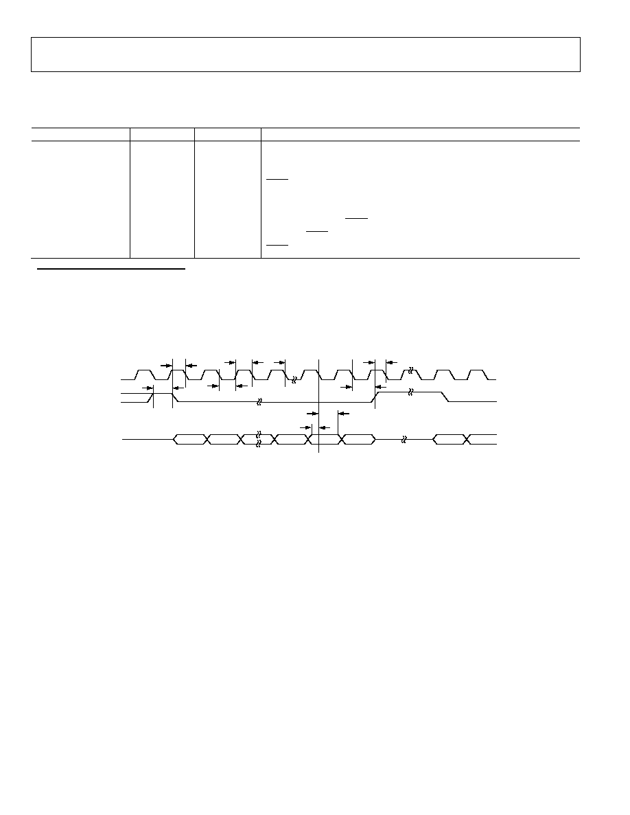
TIMING CHARACTERISTICS
V
DD
= 2.7 V to 5.5 V; all specifications T
MIN
to T
MAX
, unless otherwise noted. See Figure 2.
Table 3.
Parameter Limit
1
Unit Test
Conditions/Comments
t
1
2
33
ns min
SCLK cycle time
t
2
13
ns min
SCLK high time
t
3
12
ns min
SCLK low time
t
4
13 ns
min
SYNC to SCLK falling edge setup time
t
5
5
ns min
Data setup time
t
6
4.5
ns min
Data hold time
t
7
0 ns
min
SCLK falling edge to SYNC rising edge
t
8
33 ns
min
Minimum SYNC high time
t
9
13 ns
min
SYNC rising edge to next SCLK fall ignore
1
All input signals are specified with tr = tf = 1 ns/V (10% to 90% of V
DD
) and timed from a voltage level of (V
IL
+ V
IH
)/2.
2
Maximum SCLK frequency is 30 MHz.
t
4
t
3
t
2
t
5
t
7
t
6
D0
D1
D2
D14
D15
DIN
SYNC
SCLK
04611-A
-
002
t
9
t
1
t
8
D15
D14
Figure 2. Timing Diagram
Preliminary Technical Data
AD5641
Rev. PrC | Page 5 of 20
ABSOLUTE MAXIMUM RATINGS
T
A
= 25°C, unless otherwise noted.
Table 4.
Parameter Rating
V
DD
to GND
-0.3 V to +7.0 V
Digital Input Voltage to GND
0.3 V to V
DD
+ 0.3 V
V
OUT
to GND
0.3 V to V
DD
+ 0.3 V
Operating Temperature Range
Industrial (B Version)
40°C to +125°C
Storage Temperature Range
65°C to +160°C
Maximum Junction Temperature
150°C
SC70 Package
JA
Thermal Impedance
332°C/W
JC
Thermal Impedance
120°C/W
Lead Temperature, Soldering
Vapor Phase (60 s)
215°C
Infrared (15 s)
220°C
ESD 2.0
kV
Stresses above those listed under Absolute Maximum Ratings
may cause permanent damage to the device. This is a stress
rating only; functional operation of the device at these or any
other conditions above those listed in the operational sections
of this specification is not implied. Exposure to absolute
maximum rating conditions for extended periods may affect
device reliability.
ESD CAUTION
ESD (electrostatic discharge) sensitive device. Electrostatic charges as high as 4000 V readily accumulate on
the human body and test equipment and can discharge without detection. Although this product features
proprietary ESD protection circuitry, permanent damage may occur on devices subjected to high energy
electrostatic discharges. Therefore, proper ESD precautions are recommended to avoid performance
degradation or loss of functionality.
Document Outline
- FEATURES
- APPLICATIONS
- FUNCTIONAL BLOCK DIAGRAM
- GENERAL DESCRIPTION
- PRODUCT HIGHLIGHTS
- þÿ
- þÿ
- þÿ
- þÿ
- þÿ
- þÿ
- þÿ
- þÿ