AD5624R/AD5644R/AD5664R Quad,12-/14-/16-Bit nanoDAC® with 5 ppm/°C On-Chip Reference Data Sheet (Rev. 0)
Quad, 12-/14-/16-Bit nanoDACs
®
with
5 ppm/°C On-Chip Reference
AD5624R/AD5644R/AD5664R
Rev. 0
Information furnished by Analog Devices is believed to be accurate and reliable. However, no
responsibility is assumed by Analog Devices for its use, nor for any infringements of patents or other
rights of third parties that may result from its use. Specifications subject to change without notice. No
license is granted by implication or otherwise under any patent or patent rights of Analog Devices.
Trademarks and registered trademarks are the property of their respective owners.
One Technology Way, P.O. Box 9106, Norwood, MA 02062-9106, U.S.A.
Tel: 781.329.4700
www.analog.com
Fax: 781.461.3113
©2006 Analog Devices, Inc. All rights reserved.
FEATURES
Low power, smallest pin-compatible, quad nanoDACs
AD5664R: 16 bits
AD5644R: 14 bits
AD5624R: 12 bits
User selectable external or internal reference
External reference default
On-chip 1.25 V/2.5 V, 5 ppm/°C reference
10-lead MSOP and 3 mm × 3 mm LFCSP_WD
2.7 V to 5.5 V power supply
Guaranteed monotonic by design
Power-on reset to zero scale
Per channel power-down
Serial interface, up to 50 MHz
APPLICATIONS
Process control
Data acquisition systems
Portable battery-powered instruments
Digital gain and offset adjustment
Programmable voltage and current sources
Programmable attenuators
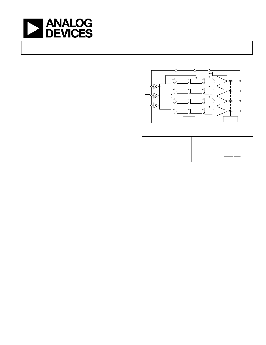
FUNCTIONAL BLOCK DIAGRAM
INTERFACE
LOGIC
SCLK
SYNC
DIN
INPUT
REGISTER
DAC
REGISTER
V
DD
GND
POWER-ON
RESET
1.25V/2.5V REF
STRING
DAC A
BUFFER
V
REFIN
/V
REFOUT
V
OUT
A
INPUT
REGISTER
DAC
REGISTER
STRING
DAC B
BUFFER
V
OUT
B
INPUT
REGISTER
DAC
REGISTER
STRING
DAC C
BUFFER
V
OUT
C
INPUT
REGISTER
DAC
REGISTER
STRING
DAC D
BUFFER
V
OUT
D
AD5624R/AD5644R/AD5664R
POWER-DOWN
LOGIC
05856-
0
01
Figure 1.
Table 1. Related Devices
Part No.
Description
AD5624/AD5664
2.7 V to 5.5 V quad,12-, 16-bit
DACs, external reference
AD5666
2.7 V to 5.5 V quad 16-bit DAC,
internal reference, LDAC, CLR pins
GENERAL DESCRIPTION
The AD5624R/AD5644R/AD5664R, members of the nanoDAC
family, are low power, quad, 12-, 14-, 16-bit buffered voltage-
out DACs. All devices operate from a single 2.7 V to 5.5 V
supply and are guaranteed monotonic by design.
The AD5624R/AD5644R/AD5664R have an on-chip reference.
The AD56x4R-3 have a 1.25 V, 5 ppm/°C reference, giving a
full-scale output range of 2.5 V; the AD56x4R-5 have a 2.5 V,
5 ppm/°C reference giving a full-scale output range of 5 V. The
on-chip reference is off at power-up allowing the use of an
external reference and all devices can be operated from a single
2.7 V to 5.5 V supply. The internal reference is enabled via a
software write.
The part incorporates a power-on reset circuit that ensures the
DAC output powers up to 0 V and remains there until a valid
write takes place. The part contains a per-channel power-down
feature that reduces the current consumption of the device to
480 nA at 5 V and provides software-selectable output loads
while in power-down mode. The low power consumption of
this part in normal operation makes it ideally suited to portable
battery-operated equipment.
The AD5624R/AD5644R/AD5664R use a versatile 3-wire serial
interface that operates at clock rates up to 50 MHz, and is
compatible with standard SPI®, QSPITM, MICROWIRETM, and
DSP interface standards. The on-chip precision output amplifier
enables rail-to-rail output swing.
PRODUCT HIGHLIGHTS
1.
Quad 12-, 14-, 16-bit DACs.
2.
On-chip 1.25 V/2.5 V, 5 ppm/°C reference.
3.
Available in 10-lead MSOP and 10-lead, 3 mm × 3 mm,
LFCSP_WD.
4.
Low power, typically consumes 1.32 mW at 3 V and
2.25 mW at 5 V.

AD5624R/AD5644R/AD5664R
Rev. 0 | Page 2 of 28
TABLE OF CONTENTS
Features .............................................................................................. 1
Applications....................................................................................... 1
Functional Block Diagram .............................................................. 1
General Description ......................................................................... 1
Product Highlights ........................................................................... 1
Revision History ............................................................................... 2
Specifications..................................................................................... 3
AD5624R-5/AD5644R-5/AD5664R-5 ....................................... 3
AD5624R-3/AD5644R-3/AD5664R-3 ....................................... 5
AC Characteristics........................................................................ 6
Timing Characteristics ................................................................ 7
Timing Diagram ........................................................................... 7
Absolute Maximum Ratings............................................................ 8
ESD Caution.................................................................................. 8
Pin Configuration and Function Descriptions............................. 9
Typical Performance Characteristics ........................................... 10
Terminology .................................................................................... 18
Theory of Operation ...................................................................... 20
D/A Section................................................................................. 20
Resistor String ............................................................................. 20
Output Amplifier........................................................................ 20
Internal
Reference ...................................................................... 20
External
Reference...................................................................... 20
Serial Interface ............................................................................ 20
Input Shift Register .................................................................... 21
SYNC Interrupt .......................................................................... 21
Power-On Reset.......................................................................... 22
Software Reset............................................................................. 22
Power-Down Modes .................................................................. 22
LDAC Function........................................................................... 23
Internal Reference Setup ........................................................... 23
Microprocessor Interfacing....................................................... 24
Applications..................................................................................... 25
Using a Reference as a Power Supply for the
AD5624R/AD5644R/AD5664R ............................................... 25
Bipolar Operation Using the AD5624R/AD5644R/AD5664R
....................................................................................................... 25
Using AD5624R/AD5644R/AD5664R with a Galvanically
Isolated Interface ........................................................................ 25
Power Supply Bypassing and Grounding................................ 26
Outline Dimensions ....................................................................... 27
Ordering Guide .......................................................................... 28
REVISION HISTORY
4/06--Revision 0: Initial Version

AD5624R/AD5644R/AD5664R
Rev. 0 | Page 3 of 28
SPECIFICATIONS
AD5624R-5/AD5644R-5/AD5664R-5
V
DD
= 4.5 V to 5.5 V; R
L
= 2 k to GND; C
L
= 200 pF to GND; V
REFIN
= V
DD
; all specifications T
MIN
to T
MAX
, unless otherwise noted.
Table 2.
B
Grade
1
Parameter Min
Typ
Max
Unit
Conditions/Comments
STATIC PERFORMANCE
2
AD5664R
Resolution 16
Bits
Relative Accuracy
±8
±16
LSB
Differential Nonlinearity
±1
LSB
Guaranteed monotonic by design
AD5644R
Resolution 14
Bits
Relative Accuracy
±2
±4
LSB
Differential Nonlinearity
±0.5
LSB
Guaranteed monotonic by design
AD5624R
Resolution 12
Bits
Relative Accuracy
±0.5
±1
LSB
Differential Nonlinearity
±0.25
LSB
Guaranteed monotonic by design
Zero-Code Error
2
10
mV
All zeroes loaded to DAC register
Offset Error
±1
±10
mV
Full-Scale Error
-0.1
±1
% of FSR
All ones loaded to DAC register
Gain Error
±1.5
% of FSR
Zero-Code Error Drift
±2
V/°C
Gain Temperature
Coefficient
±2.5
ppm
Of FSR/°C
DC Power Supply Rejection
Ratio
-100
dB
DAC code = midscale ; V
DD
= 5 V ± 10%
DC Crosstalk
(External Reference)
10
V
Due to full-scale output change,
R
L
= 2 k to GND or V
DD
10
V/mA
Due to load current change
5
V
Due to powering down (per channel)
DC Crosstalk
(Internal Reference)
25
V
Due to full-scale output change,
R
L
= 2 k to GND or V
DD
20
V/mA
Due to load current change
10
V
Due to powering down (per channel)
OUTPUT CHARACTERISTICS
3
Output Voltage Range
0
V
DD
V
Capacitive Load Stability
2
nF
R
L
=
10
nF
R
L
= 2 k
DC Output Impedance
0.5
Short-Circuit Current
30
mA
V
DD
= 5 V
Power-Up Time
4
s
Coming out of power-down mode; V
DD
= +5 V
REFERENCE INPUTS
Reference Current
170
200
A
V
REF
= V
DD
= 5.5 V
Reference Input Range
0.75
V
DD
V
Reference Input Impedance
26
k
REFERENCE OUTPUT
Output Voltage
2.495
2.505
V
At ambient
Reference TC
3
±5
±10
ppm/°C
Output Impedance
7.5
k

AD5624R/AD5644R/AD5664R
Rev. 0 | Page 4 of 28
B
Grade
1
Parameter Min
Typ
Max
Unit
Conditions/Comments
LOGIC INPUTS
3
Input Current
±2
A
All digital inputs
V
INL
, Input Low Voltage
0.8
V
V
DD
= 5 V
V
INH
, Input High Voltage
2
V
V
DD
= 5 V
Pin Capacitance
3
pF
POWER REQUIREMENTS
V
DD
4.5
5.5
V
I
DD
(Normal Mode)
4
V
IH
= V
DD
, V
IL
= GND
V
DD
= 4.5 V to 5.5 V
0.45
0.9
mA
Internal reference off
V
DD
= 4.5 V to 5.5 V
0.95
1.2
mA
Internal reference on
I
DD
(All Power-Down Modes)
5
V
IH
= V
DD
, V
IL
= GND
V
DD
= 4.5 V to 5.5 V
0.48
1
A
1
Temperature range: B grade: -40°C to +105°C.
2
Linearity calculated using a reduced code range: AD5664R (Code 512 to Code 65,024); AD5644R (Code 128 to Code 16,256); AD5624R (Code 32 to Code 4064). Output
unloaded.
3
Guaranteed by design and characterization, not production tested.
4
Interface inactive. All DACs active. DAC outputs unloaded.
5
All DACs powered down.

AD5624R/AD5644R/AD5664R
Rev. 0 | Page 5 of 28
AD5624R-3/AD5644R-3/AD5664R-3
V
DD
= 2.7 V to 3.6 V; R
L
= 2 k to GND; C
L
= 200 pF to GND; V
REFIN
= V
DD
; all specifications T
MIN
to T
MAX
, unless otherwise noted.
Table 3.
B
Grade
1
Parameter Min
Typ
Max
Unit
Conditions/Comments
STATIC PERFORMANCE
2
AD5664R
Resolution 16
Bits
Relative Accuracy
±8
±16
LSB
Differential Nonlinearity
±1
LSB
Guaranteed monotonic by design
AD5644R
Resolution 14
Bits
Relative Accuracy
±2
±4
LSB
Differential Nonlinearity
±0.5
LSB
Guaranteed monotonic by design
AD5624R
Resolution 12
Bits
Relative Accuracy
±0.5
±1
LSB
Differential Nonlinearity
±0.25
LSB
Guaranteed monotonic by design
Zero-Code Error
2
10
mV
All zeroes loaded to DAC register
Offset Error
±1
±10
mV
Full-Scale Error
-0.1
±1
% of FSR
All ones loaded to DAC register
Gain Error
±1.5
% of FSR
Zero-Code Error Drift
±2
V/°C
Gain Temperature
Coefficient
±2.5
ppm
Of FSR/°C
DC Power Supply Rejection
Ratio
-100
dB
DAC code = midscale; V
DD
= 3 V ± 10%
DC Crosstalk
(External Reference)
10
V
Due to full-scale output change,
R
L
= 2 k to GND or V
DD
10
V/mA
Due to load current change
5
V
Due to powering down (per channel)
DC Crosstalk
(Internal Reference)
25
V
Due to full-scale output change,
R
L
= 2 k to GND or V
DD
20
V/mA
Due to load current change
10
V
Due to powering down (per channel)
OUTPUT CHARACTERISTICS
3
Output Voltage Range
0
V
DD
V
Capacitive Load Stability
2
nF
R
L
=
10
nF
R
L
= 2 k
DC Output Impedance
0.5
Short-Circuit Current
30
mA
V
DD
= 3 V
Power-Up Time
4
s
Coming out of power-down mode; V
DD
= 3 V
REFERENCE INPUTS
Reference Current
170
200
A
V
REF
= V
DD
= 3.6 V
Reference Input Range
0
V
DD
V
Reference Input Impedance
26
k
REFERENCE OUTPUT
Output Voltage
1.247
1.253
V
At ambient
Reference TC
3
±5
±15
ppm/°C
Output Impedance
7.5
k
Document Outline
- þÿ
- þÿ
- FUNCTIONAL BLOCK DIAGRAM
- þÿ
- þÿ
- þÿ
- þÿ
- þÿ
- þÿ
- þÿ
- þÿ
- TIMING CHARACTERISTICS
- þÿ
- þÿ
- þÿ
- þÿ
- þÿ
- þÿ
- þÿ
- þÿ
- þÿ
- þÿ
- þÿ
- þÿ
- þÿ
- SYNC INTERRUPT
- þÿ
- þÿ
- þÿ
- þÿ
- þÿ
- þÿ
- þÿ
- þÿ
- þÿ
- þÿ
- POWER SUPPLY BYPASSING AND GROUNDING
- þÿ