
5 V 18-Bit nanoDAC
TM
in an SOT-23
Preliminary Technical Data
AD5680
Rev. PrA
Information furnished by Analog Devices is believed to be accurate and reliable. However, no
responsibility is assumed by Analog Devices for its use, nor for any infringements of patents or other
rights of third parties that may result from its use. Specifications subject to change without notice. No
license is granted by implication or otherwise under any patent or patent rights of Analog Devices.
Trademarks and registered trademarks are the property of their respective owners.
One Technology Way, P.O. Box 9106, Norwood, MA 02062-9106, U.S.A.
Tel: 781.329.4700
www.analog.com
Fax: 781.461.3113
©2006 Analog Devices, Inc. All rights reserved.
FEATURES
Single 18-bit nanoDAC
18-bit monotonic
12-bit accuracy guaranteed
Tiny 8-lead SOT-23 package
Power-on reset to zero scale/midscale
4.5 V to 5.5 V power supply
Serial interface
Rail-to-rail operation
SYNC interrupt facility
Temperature range -40∞C to +105∞C
APPLICATIONS
Closed loop process control
Low bandwidth data acquisition systems
Portable battery-powered instruments
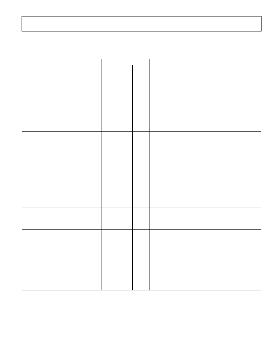
FUNCTIONAL BLOCK DIAGRAM
V
OUT
V
FB
V
DD
GND
V
REF
AD5680
18-BIT
DAC
REF(+)
POWER-ON
RESET
DAC
REGISTER
INPUT
CONTROL
LOGIC
DIN
SCLK
SYNC
05854-
001
OUTPUT
BUFFER
Figure 1.
GENERAL DESCRIPTION
The AD5680, a member of the nanoDAC family, is a single,
18-bit buffered voltage-out DAC that operates from a single
4.5 V to 5.5 V supply and is 18 bit monotonic .
The AD5680 requires an external reference voltage to set the
output range of the DAC. The part incorporates a power-on
reset circuit that ensures the DAC output powers up to 0 V
(AD5680-1) or to midscale (AD5680-2), and remains there
until a valid write takes place.
The low power consumption of this part in normal operation
makes it ideally suited to portable battery-operated equipment.
The power consumption is 2.5mW at 5 V.
The AD5680's on-chip precision output amplifier allows rail-to-
rail output swing to be achieved. For remote sensing applications,
the output amplifier's inverting input is available to the user.
The AD5680 uses a versatile 3-wire serial interface that operates
at clock rates up to 30 MHz, and is compatible with standard
SPIÆ, QSPITM, MICROWIRETM, and DSP interface standards.
PRODUCT HIGHLIGHTS
1. 18 bits of resolution; ±1lSBs DNL
2. 12-bit accuracy guaranteed for 18-bit DAC.
3. Available in an 8-lead SOT-23.
4. Low power. Typically consumes 2.5 mW at 5 V.
5. Power-on reset to zero scale or to midscale.
RELATED DEVICES
Table 1.
Part No.
Description
AD5662
16-bit DAC in SOT-23

AD5680
Preliminary Technical Data
Rev. PrA | Page 2 of 21
TABLE OF CONTENTS
Specifications..................................................................................... 3
Timing Characteristics..................................................................... 4
Absolute Maximum Ratings............................................................ 5
ESD Caution.................................................................................. 5
Pin Configuration and Function Description .............................. 6
Typical Performance Characteristics ............................................. 7
Terminology .................................................................................... 12
Theory of Operation ...................................................................... 13
DAC Section................................................................................ 13
Resistor String ............................................................................. 13
Output Amplifier........................................................................ 13
Interpolator Architecture .......................................................... 13
Serial Interface ............................................................................ 14
Input Shift Register .................................................................... 14
SYNC Interrupt .......................................................................... 14
Power-On Reset.......................................................................... 14
Microprocessor Interfacing....................................................... 15
Applications..................................................................................... 16
Closed Loop applications .......................................................... 16
Filter ............................................................................................. 16
Choosing a Reference for the AD5680.................................... 16
Using a Reference as a Power Supply for the AD5680 .......... 18
Using AD5680 with a Galvanically Isolated Interface........... 18
Power Supply Bypassing and Grounding................................ 18
Outline Dimensions ....................................................................... 19
Ordering Guide .......................................................................... 19
REVISION HISTORY
3/06--Preliminary Revision A
Preliminary Technical Data
AD5680
Rev. PrA | Page 3 of 21
SPECIFICATIONS
V
DD
= 4.5 V to 5.5 V; R
L
= 2 k to GND; C
L
= 200 pF to GND; V
REF
= V
DD
; all specifications T
MIN
to T
MAX
, unless otherwise noted.
Table 1.
B
Grade
B
Version
1
Parameter Min
Typ
Max
Unit
Conditions/Comments
STATIC PERFORMANCE
2
Resolution 18
Bits
Relative Accuracy
±64
LSB
See Figure 4
Differential Nonlinearity
±1
LSB
See Figure 5
Zero-Code Error
2
10
mV
All 0s loaded to DAC register
Full-Scale Error
-0.2
-1
% FSR
All 1s loaded to DAC register
Offset Error
±10
mV
Gain Error
±1.5
% FSR
Zero-Code Error Drift
3
±2
µV/∞C
Gain Temperature Coefficient
3
±2.5
ppm
Of
FSR/∞C
DC Power Supply Rejection Ratio
3
-100
dB
DAC code = midscale; V
DD
= 5 V ± 10%
OUTPUT CHARACTERISTICS
3
Output Voltage Range
0
V
DD
V
Output Voltage Settling Time
80
85
µs
º to æ scale change settling to ±8 LSB
R
L
= 2 k; 0 pF < C
L
< 200 pF
Slew Rate
1.5
V/µs
º to æ scale
Capacitive Load Stability
2
nF
R
L
=
10
nF
R
L
= 2 k
Output Noise Spectral Density
4
80
nV/Hz
DAC code = midscale,10 kHz
Output Noise (0.1 Hz to 10 Hz)
4
25
µV p-p
DAC code = midscale
Total Harmonic Distortion (THD)
4
-80
dB
V
REF
= 2 V ± 300 mV p-p, f = 200Hz
Digital-to-Analog Glitch Impulse
5
nV-s
1 LSB change around major carry
Digital Feedthrough
0.2
nV-s
DC Output Impedance
0.5
Short-Circuit Current
4
30
mA
V
DD
= 5 V
REFERENCE INPUT
3
Reference Current
40
75
µA
V
REF
= V
DD
= 5 V
Reference Input Range
5
0.75
V
DD
V
Reference Input Impedance
125
k
LOGIC INPUTS
3
Input Current
±2
µA
All digital inputs
V
INL
, Input Low Voltage
0.8
V
V
DD
= 5 V
V
INH
, Input High Voltage
2
V
V
DD
= 5 V
Pin Capacitance
3
pF
POWER REQUIREMENTS
V
DD
4.5
5.5
V
All digital inputs at 0 V or V
DD
I
DD
(Normal Mode)
DAC active and excluding load current
V
DD
= 4.5 V to 5.5 V
0.5
1
mA
V
IH
= V
DD
and V
IL
= GND
POWER EFFICIENCY
I
OUT
/I
DD
85
%
I
LOAD
= 2 mA, V
DD
= 5 V
1
Temperature range for B version is -40∞C to +105∞C, typical at +25∞C.
2
DC specifications tested with the outputs unloaded, unless otherwise stated. Linearity calculated using a reduced code range of 2048 to 260096. Measured in system
bandwidth of tbd.
3
Guaranteed by design and characterization; not production tested.
4
Output unloaded.
5
Reference input range at ambient where ±1 LSB maximum DNL specification is achievable.
AD5680
Preliminary Technical Data
Rev. PrA | Page 4 of 21
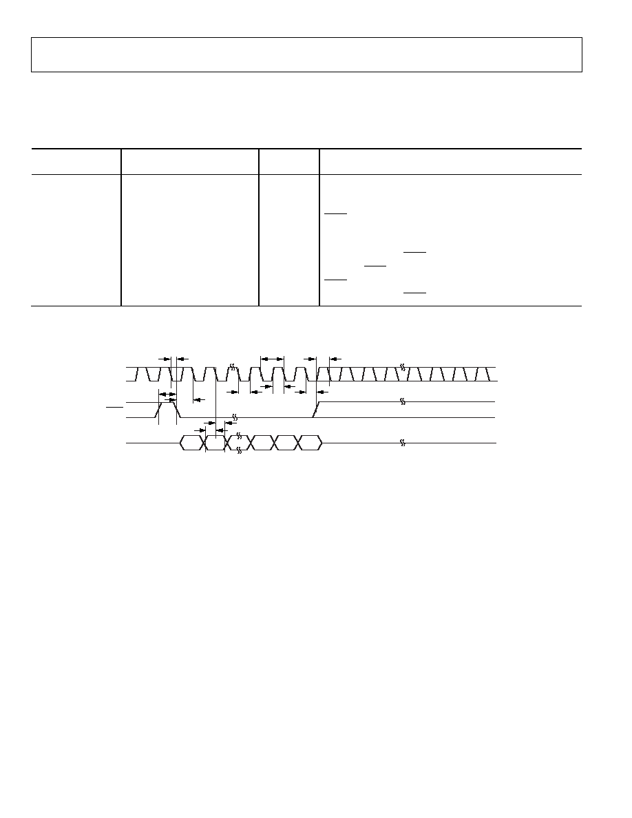
TIMING CHARACTERISTICS
All input signals are specified with tr = tf = 1 ns/V (10% to 90% of V
DD
) and timed from a voltage level of (V
IL
+ V
IH
)/2. See Figure 2.
V
DD
= 4.5 V to 5.5 V; all specifications T
MIN
to T
MAX
, unless otherwise noted.
Table 2.
Limit
at
T
MIN
, T
MAX
Parameter V
DD
= 4.5 V to 5.5 V
Unit
Conditions/Comments
t
1
1
33
ns min
SCLK cycle time
t
2
13
ns min
SCLK high time
t
3
13
ns min
SCLK low time
t
4
13
ns
min
SYNC to SCLK falling edge setup time
t
5
5
ns min
Data setup time
t
6
4.5
ns min
Data hold time
t
7
0
ns
min
SCLK falling edge to SYNC rising edge
t
8
33
ns
min
Minimum SYNC high time
t
9
13
ns
min
SYNC rising edge to SCLK fall ignore
t
10
0
ns
min
SCLK falling edge to SYNC fall ignore
1
Maximum SCLK frequency is 30 MHz at V
DD
= 4.5 V to 5.5 V.
DIN
SYNC
SCLK
DB23
DB0
t
9
t
10
t
4
t
3
t
2
t
7
t
6
t
5
t
1
t
8
05
85
4-
00
2
Figure 2. Serial Write Operation
Preliminary Technical Data
AD5680
Rev. PrA | Page 5 of 21
ABSOLUTE MAXIMUM RATINGS
T
A
= 25∞C, unless otherwise noted.
Table 3.
Parameter Rating
V
DD
to GND
-0.3 V to +7 V
V
OUT
to GND
-0.3 V to V
DD
+ 0.3 V
V
FB
to GND
-0.3 V to V
DD
+ 0.3 V
V
REF
to GND
-0.3 V to V
DD
+ 0.3 V
Digital Input Voltage to GND
-0.3 V to V
DD
+ 0.3 V
Operating Temperature Range
Industrial (B Version)
-40∞C to +105∞C
Storage Temperature Range
-65∞C to +150∞C
Junction Temperature (T
J
max) 150∞C
Power Dissipation
(T
J
max - T
A
)/
JA
SOT-23 Package (4-Layer Board)
JA
Thermal Impedance
119∞C/W
Reflow Soldering Peak Temperature
Pb-free
260∞C
Stresses above those listed under Absolute Maximum Ratings
may cause permanent damage to the device. This is a stress
rating only; functional operation of the device at these or any
other conditions above those indicated in the operational
section of this specification is not implied. Exposure to absolute
maximum rating conditions for extended periods may affect
device reliability.
ESD CAUTION
ESD (electrostatic discharge) sensitive device. Electrostatic charges as high as 4000 V readily accumulate on the
human body and test equipment and can discharge without detection. Although this product features
proprietary ESD protection circuitry, permanent damage may occur on devices subjected to high energy
electrostatic discharges. Therefore, proper ESD precautions are recommended to avoid performance
degradation or loss of functionality.