 | –≠–ª–µ–∫—Ç—Ä–æ–Ω–Ω—ã–π –∫–æ–º–ø–æ–Ω–µ–Ω—Ç: AD569K | –°–∫–∞—á–∞—Ç—å:  PDF PDF  ZIP ZIP |
FUNCTIONAL BLOCK DIAGRAM
REV. A
Information furnished by Analog Devices is believed to be accurate and
reliable. However, no responsibility is assumed by Analog Devices for its
use, nor for any infringements of patents or other rights of third parties
which may result from its use. No license is granted by implication or
otherwise under any patent or patent rights of Analog Devices.
a
16-Bit Monotonic
Voltage Output D/A Converter
AD569
FEATURES
Guaranteed 16-Bit Monotonicity
Monolithic BiMOS II Construction
0.01% Typical Nonlinearity
8- and 16-Bit Bus Compatibility
3 s Settling to 16 Bits
Low Drift
Low Power
Low Noise
APPLICATIONS
Robotics
Closed-Loop Positioning
High-Resolution ADCs
Microprocessor-Based Process Control
MIL-STD-883 Compliant Versions Available
PRODUCT DESCRIPTION
The AD569 is a monolithic 16-bit digital-to-analog converter
(DAC) manufactured in Analog Devices' BiMOS II process.
BiMOS II allows the fabrication of low power CMOS logic
functions on the same chip as high precision bipolar linear cir-
cuitry. The AD569 chip includes two resistor strings, selector
switches decoding logic, buffer amplifiers, and double-buffered
input latches.
The AD569's voltage-segmented architecture insures 16-bit
monotonicity over time and temperature. Integral nonlinearity is
maintained at
±
0.01%, while differential nonlinearity is
±
0.0004%. The on-chip, high-speed buffer amplifiers provide a
voltage output settling time of 3
µ
s to within
±
0.001% for a
full-scale step.
The reference input voltage which determines the output range
can be either unipolar or bipolar. Nominal reference range is
±
5 V and separate reference force and sense connections are
provided for high accuracy applications. The AD569 can oper-
ate with an ac reference in multiplying applications.
Data may be loaded into the AD569's input latches from 8- and
16-bit buses. The double-buffered structure simplifies 8-bit bus
interfacing and allows multiple DACs to be loaded asynchro-
nously and updated simultaneously. Four TTL/LSTTL/5 V
CMOS-compatible signals control the latches: CS, LBE, HBE,
and LDAC
The AD569 is available in five grades: J and K versions are
specified from 0
∞
C to +70
∞
C and are packaged in a 28-pin plas-
tic DIP and 28-pin PLCC package; AD and BD versions are
specified from ≠25
∞
C to +85
∞
C and are packaged in a 28-pin
ceramic DIP. The SD version, also in a 28-pin ceramic DIP, is
specified from ≠55
∞
C to +125
∞
C.
One Technology Way, P.O. Box 9106, Norwood, MA 02062-9106, U.S.A.
Tel: 617/329-4700
Fax: 617/326-8703
PRODUCT HIGHLIGHTS
1. Monotonicity to 16 bits is insured by the AD569's voltage-
segmented architecture.
2. The output range is ratiometric to an external reference or ac
signal. Gain error and gain drift of the AD569 are negligible.
3. The AD569's versatile data input structure allows loading
from 8- and 16-bit buses.
4. The on-chip output buffer amplifier can supply
±
5 V into a
1 k
load, and can drive capacitive loads of up to 1000 pF.
5. Kelvin connections to the reference inputs preserve the gain
and offset accuracy of the transfer function in the presence of
wiring resistances and ground currents.
6. The AD569 is available in versions compliant with MIL-STD-
883. Refer to the Analog Devices Military Products Data-
book or current AD569/883B data sheet for detailed
specifications.

AD569≠SPECIFICATIONS
Model
AD569JN/JP/AD
AD569KN/KP/BD
AD569SD
Parameter
Min
Typ
Max
Min
Typ
Max
Min
Typ
Max
Units
RESOLUTION
16
16
16
Bits
LOGIC INPUTS
V
IH
(Logic "l")
2.0
5.5
2.0
5.5
2.0
5.5
Volts
V
IL
(Logic "0")
0
0.8
0
0.8
0
0.8
Volts
I
IH
(V
IH
= 5.5 V)
10
10
10
µ
A
I
IL
(V
IL
= 0 V)
10
10
10
µ
A
TRANSFER FUNCTION
CHARACTERISTICS
Integral Nonlinearity
±
0.02
0.04
±
0.01
0.024
0.04
% FSR
1
T
MIN
to T
MAX
±
0.02
0.04
±
0.020
0.024
0.04
% FSR
Differential Nonlinearity
±
1/2
1
±
1/4
1/2
1
LSB
T
MIN
to T
MAX
±
1/2
1
±
1/2
1
1
LSB
Unipolar Offset
2
500
350
500
µ
V
T
MIN
to T
MAX
750
450
750
µ
V
Bipolar Offset
2
500
350
500
µ
V
T
MIN
to T
MAX
750
450
750
µ
V
Full Scale Error
2
350
350
350
µ
V
T
MIN
to T
MAX
750
750
750
µ
V
Bipolar Zero
2
0.04
0.024
0.04
% FSR
T
MIN
to T
MAX
0.04
0.024
0.04
% FSR
REFERENCE INPUT
+V
REF
Range
3
≠5
+5
≠5
+5
≠5
+5
Volts
≠V
REF
Range
≠5
+5
≠5
+5
≠5
+5
Volts
Resistance
15
20
25
15
20
25
15
20
25
k
4
OUTPUT CHARACTERISTICS
Voltage
≠5
+5
≠5
+5
≠5
+5
Volts
Capacitive Load
1000
1000
1000
pF
Resistive Load
1
1
1
k
Short Circuit Current
10
10
10
mA
POWER SUPPLIES
Voltage
+V
S
+10.8
+12
+13.2
+10.8
+12
+13.2
+10.8
+12
+13.2
Volts
≠V
S
≠10.8
≠12
≠13.2
≠10.8
≠12
≠13.2
≠10.8
≠12
≠13.2
Volts
Current
+I
S
+9
+13
+9
+13
+9
+13
mA
≠I
S
≠9
≠13
≠9
≠13
≠9
≠13
mA
Power Supply Sensitivity
5
+10.8 V
+V
S
+13.2 V
±
0.5
2
±
0.5
2
±
0.5
2
ppm/%
≠10.8 V
≠V
S
≠13.2 V
±
1
3
±
1
3
±
1
3
ppm/%
TEMPERATURE RANGE
Specified
JN, KN, JP, KP
0
+70
0
+70
∞
C
AD, BD
≠25
+85
≠25
+85
∞
C
SD
≠55
+125
∞
C
Storage
JN, KN, JP, KP
≠65
+150
≠65
+150
∞
C
AD, BD, SD
≠65
+150
≠65
+150
≠65
+150
∞
C
NOTES
1
FSR stands for Full-Scale Range, and is 10 V for a ≠5 V to +5 V span.
2
Refer to Definitions section.
3
For operation with supplies other than
±
12 V, refer to the Power Supply and Reference Voltage Range Section.
4
Measured between +V
REF
Force and ≠V
REF
Force.
5
Sensitivity of Full-Scale Error due to changes in +V
S
and sensitivity of Offset to changes in ≠V
S
.
Specifications subject to change without notice.
Specifications shown in boldface are tested on all production units at final electrical test. Results from those tests are used to calculate outgoing quality levels. All min
and max specifications are guaranteed, although only those shown in boldface are tested on all production units.
(T
A
= +25 C, +V
S
= +12 V, ≠V
S
= ≠12 V, +V
REF
= +5 V, ≠V
REF
= ≠5 V, unless
otherwise noted.)
REV. A
≠2≠
AD569
REV. A
≠3≠
AC PERFORMANCE CHARACTERISTICS
These characteristics are included for Design Guidance Only and are not subject to test.
+V
S
= +12 V; ≠V
S
= ≠12 V; +V
REF
= +5 V; ≠V
REF
= ≠5 V excepts where stated.
Parameter
Limit
Units
Test Conditions/Comments
Output Voltage Settling
5
µ
s max
No Load Applied
(Time to
±
0.001% FS
3
µ
s typ
(DAC output measured from falling edge of LDAC.)
For FS Step)
6
µ
s max
V
OUT
Load = 1 k
, C
LOAD
= 1000 pF.
4
µ
s typ
(DAC output measured from falling edge of LDAC. )
Digital-to-Analog Glitch
500
nV-sec typ
Measured with V
REF
= 0 V. DAC registers alternatively loaded
Impulse
with input codes of 8000
H
and 0FFF
H
(worst-case
transition). Load = 1 k
.
Multiplying Feedthrough
≠100
dB max
+V
REF
= 1 V rms 10 kHz sine wave,
≠V
REF
= 0 V
Output Noise Voltage
40
nV/
Hz
typ
Measured between V
OUT
and ≠V
REF
Density (1 kHz-1 MHz)
TIMING CHARACTERISTICS
(+V
S
= +12 V, ≠V
S
= ≠12 V, V
IH
= 2.4 V, V
IL
= 0.4 V,T
MIN
to T
MAX
)
Parameter
Limit
Units
Test Conditions/Comments
Case A
150 ns Pulse on HBE, LBE, and LDAC
T
HS
= 140 ns min, T
HH
= 10 ns min
t
WC
120
ns min
CS
Pulse Width
t
SC
60
ns min
CS
Data Setup Time
t
HC
20
ns min
CS
Data Hold Time
Case B
None
t
WB
70
ns min
HBE
, LBE Pulse Width
t
SB
80
ns min
HBE
, LBE Data Setup Time
t
HB
20
ns min
HBE
, LBE Data Hold Time
t
SCS
120
ns min
CS
Setup Time
t
HCS
10
ns min
CS
Hold Time
t
WD
120
ns min
LDAC
Pulse Width
Case C
None
t
WB
120
ns min
HBE
, LBE Pulse Width
t
SB
80
ns min
HBE
, LBE Data Setup Time
t
HB
20
ns min
HBE
, LBE Data Hold Time
t
SCS
120
ns min
CS
Setup Time
t
HCS
10
ns min
CS
Hold Time
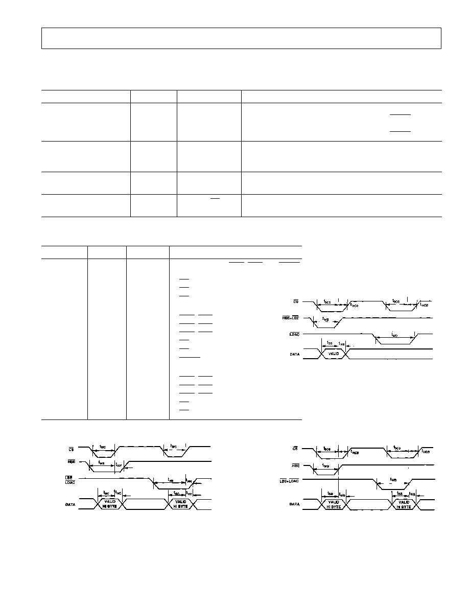
Figure 2a. AD569 Timing Diagram ≠ Case B
Figure 2b. AD569 Timing Diagram ≠ Case C
Figure 1. AD569 Timing Diagram ≠ Case A

AD569
REV. A
≠4≠
ABSOLUTE MAXIMUM RATINGS*
(T
A
= +25
∞
C unless otherwise noted)
+V
S
(Pin 1) to GND (Pin 18) . . . . . . . . . . . . . . +18 V, ≠0.3 V
≠V
S
(Pin 28) to GND (Pin 18) . . . . . . . . . . . . . . ≠18 V, +0.3 V
+V
S
(Pin 1) to ≠V
S
(Pin 28) . . . . . . . . . . . . . . . +26.4 V, ≠0.3 V
Digital Inputs
(Pins 4-14, 19-27) to GND (Pin 18) . . . . . . . . . +V
S
, ≠0.3 V
+V
REF
Force (Pin 3) to +V
REF
Sense (Pin 2) . . . . . . . .
±
16.5 V
≠V
REF
Force (Pin 15) to ≠V
REF
Sense (Pin 16) . . . . . . .
±
16.5 V
V
REF
Force (Pins 3, 15) to GND (Pin 18) . . . . . . . . . . . . .
±
V
S
V
REF
Sense (Pins 2, 16) to GND (Pin 18) . . . . . . . . . . . . .
±
V
S
V
OUT
(Pin 17) . . . . . . . . . . . . . . . . . . Indefinite Short to GND
. . . . . . . . . . . . . . . . . . . . . . . .
Momentary Short to +V
S,
≠V
S
Power Dissipation (Any Package) . . . . . . . . . . . . . . . 1000 mW
Operating Temperature Range
Commercial Plastic (JN, KN, JP, KP Versions) 0
∞
C to +70
∞
C
Industrial Ceramic (AD, BD Versions) . . . . ≠25
∞
C to +85
∞
C
Extended Ceramic (SD Versions) . . . . . . . ≠55
∞
C to +125
∞
C
Storage Temperature . . . . . . . . . . . . . . . . . . . ≠65
∞
C to +150
∞
C
Lead Temperature Range (Soldering, 10 secs) . . . . . . . +300
∞
C
*Stresses above those listed under "Absolute Maximum Ratings" may cause
permanent damage to the device. This is a stress rating only and functional
operation of the device at these or any other conditions above those indicated in the
operational sections of this specification is not implied. Exposure to absolute
maximum rating conditions for extended periods may affect device reliability.
ESD SENSITIVITY
The AD569 features input protection circuitry consisting of large "distributed" diodes and polysilicon
series resistors to dissipate both high-energy discharges (Human Body Model) and fast, low-energy
pulses (Charged Device Model). Per Method 3015.2 of MIL-STD-883C, the AD569 has been
classified as a Category A device.
Proper ESD precautions are strongly recommended to avoid functional damage or performance
degradation. Charges as high as 4000 volts readily accumulate on the human body and test equipment
and discharge without detection. Unused devices must be stored in conductive foam or shunts, and
the foam should be discharged to the destination socket before devices are removed. For further
information on ESD precautions, refer to Analog Devices' ESD Prevention Manual.
PIN DESIGNATIONS
ORDERING GUIDE
Integral Nonlinearity
Differential Nonlinearity
Temperature
Package
Model
1
+25 C
T
MIN
≠T
MAX
+25 C
T
MIN
≠T
MAX
Range
Option
2
AD569JN
±
0.04%
±
0.04%
±
1 LSB
±
1 LSB
0
∞
C to +70
∞
C
N-28
AD569JP
±
0.04%
±
0.04%
±
1 LSB
±
1 LSB
0
∞
C to +70
∞
C
P-28A
AD569KN
±
0.024%
±
0.024%
±
1/2 LSB
±
1 LSB
0
∞
C to +70
∞
C
N-28
AD569KP
±
0.024%
±
0.024%
±
1/2 LSB
±
1 LSB
0
∞
C to +70
∞
C
P-28A
AD569AD
±
0.04%
±
0.04%
±
1 LSB
±
1 LSB
≠25
∞
C to +85
∞
C
D-28
AD569BD
±
0.024%
±
0.024%
±
1/2 LSB
±
1 LSB
≠25
∞
C to +85
∞
C
D-28
AD569SD
±
0.04%
±
0.04%
±
1 LSB
±
1 LSB
≠55
∞
C to +125
∞
C
D-28
NOTES
1
For details on grade and package offerings screened in accordance with MIL-STD-883, refer to the Analog Devices Military Products Databook
or current AD569/883B data sheet.
2
D = Ceramic DIP; N = Plastic DIP; P = Plastic Leaded Chip Carrier.
WARNING!
ESD SENSITIVE DEVICE

AD569
REV. A
≠5≠
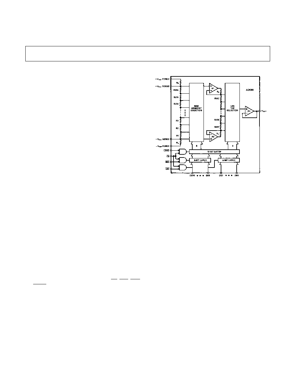
Figure 3. AD569 Block Diagram
FUNCTIONAL DESCRIPTION
The AD569 consists of two resistor strings, each of which is di-
vided into 256 equal segments (see Figure 3). The 8 MSBs of
the digital input word select one of the 256 segments on the first
string. The taps at the top and bottom of the selected segment
are connected to the inputs of the two buffer amplifiers A1 and
A2. These amplifiers exhibit extremely high CMRR and low
bias current, and thus accurately preserve the voltages at the top
and bottom of the segment. The buffered voltages from the seg-
ment endpoints are applied across the second resistor string,
where the 8LSBs of the digital input word select one of the 256
taps. Output amplifier A3 buffers this voltage and delivers it to
the output.
Buffer amplifiers A1 and A2 leap-frog up the first string to pre-
serve monotonicity at the segment boundaries. For example,
when increasing the digital code from 00FF
H
to 0100
H
, (the first
segment boundary), A1 remains connected to the same tap on
the first resistor, while A2 jumps over it and is connected to the
tap which becomes the top of the next segment. This design
guarantees monotonicity even if the amplifiers have offset volt-
ages. In fact, amplifier offset only contributes to integral linear-
ity error.
CAUTION
It is generally considered good engineering practice to avoid
inserting integrated circuits into powered-up sockets. This
guideline is especially important with the AD569. An empty,
powered-up socket configures external buffer amplifiers in an
open-loop mode, forcing their outputs to be at the positive or
negative rail. This condition may result in a large current surge
between the reference force and sense terminals. This current
surge may permanently damage the AD569.
ANALOG CIRCUIT DETAILS
MONOTONICITY: A DAC is monotonic if the output either
increases or remains constant for increasing digital inputs. All
versions of the AD569 are monotonic over their full operating
temperature range.
DIFFERENTIAL NONLINEARITY: DNL is the measure of
the change in the analog output, normalized to full scale, associ-
ated: with a 1 LSB change in the digital input code. Monotonic
behavior requires that the differential linearity error be less than
1 LSB over the temperature range of interest. For example, for a
±
5 V output range, a change of 1 LSB in digital input code
should result in a 152
µ
V change in the analog output (1 LSB =
10 V/65,536). If the change is actually 38
µ
V, however, the dif-
ferential linearity error would be ≠114
µ
V, or ≠3/4 LSB. By leap-
frogging the buffer amplifier taps on the first divider, a typical
AD569 keeps DNL within
±
38
µ
V (
±
1/4 LSB) around each of
the 256 segment boundaries defined by the upper byte of the in-
put word (see Figure 5). Within the second divider, DNL also
typically remains less than
±
38
µ
V as shown in Figure 6. Since
the second divider is independent of absolute voltage, DNL is
the same within the rest of the 256 segments.
OFFSET ERROR: The difference between the actual analog
output and the ideal output (≠V
REF
), with the inputs loaded with
all zeros is called the offset error. For the AD569, Unipolar Off-
set is specified with 0 V applied to ≠V
REF
and Bipolar Offset is
specified with ≠5 V applied to ≠V
REF
. Either offset is trimmed by
adjusting the voltage applied to the ≠V
REF
terminals.
BIPOLAR ZERO ERROR: The deviation of the analog output
from the ideal half-scale output of 0.0000 V when the inputs are
loaded with 8000
H
is called the Bipolar Zero Error. For the
AD569, it is specified with
±
5 V applied to the reference
terminals.
Definitions
LINEARITY ERROR: Analog Devices defines linearity error as
the maximum deviation of the actual, adjusted DAC output
from the ideal output (a straight line drawn from 0 to FS≠1LSB)
for any bit combination. The AD569's linearity is primarily lim-
ited by resistor uniformity in the first divider (upper byte of
16-bit input). The plot in Figure 4 shows the AD569's typical
linearity error across the entire output range to be within
±
0.01% of full scale. At 25
∞
C the maximum linearity error for
the AD569JN, AD and SD grades is specified to be
±
0.04%,
and
±
0.024% for the KN and BD versions.
Figure 4. Typical Linearity