 | ÐлекÑÑоннÑй компоненÑ: AD5764ASU | СкаÑаÑÑ:  PDF PDF  ZIP ZIP |
AD5744/AD5764 Complete, Quad, 14/16-Bit, High Accuracy, Serial Input, Bipolar Voltage Output DAC Preliminary Data Sheet (Rev. PrA)

Complete, Quad, 14/16-Bit, High Accuracy,
Serial Input, Bipolar Voltage Output DAC
i
CMOS
TM
Preliminary Technical Data
Rev. PrA
15-Nov-04
Information furnished by Analog Devices is believed to be accurate and reliable.
However, no responsibility is assumed by Analog Devices for its use, nor for any
infringements of patents or other rights of third parties that may result from its use.
Specifications subject to change without notice. No license is granted by implication
or otherwise under any patent or patent rights of Analog Devices. Trademarks and
registered trademarks are the property of their respective owners.
One Technology Way, P.O. Box 9106, Norwood, MA 02062-9106, U.S.A.
Tel: 781.329.4700
www.analog.com
Fax: 781.326.8703
© 2004 Analog Devices, Inc. All rights reserved.
FEATURES
Complete quad 14/16-bit D/A converter
Programmable output range: ±10 V, ±10.25 V, or ±10.5 V
±1 LSB max INL error, ±1 LSB max DNL error
Low noise : 60 nV/Hz
Settling time: 10µs max
Integrated reference buffers
Internal reference, 10 ppm/°C
On-chip temp sensor, ±5°C accuracy
Output control during power-up/brownout
Programmable short-circuit protection
Simultaneous updating via LDAC
Asynchronous CLR to zero code
Digital offset and gain adjust
Logic output control pins
DSP/microcontroller compatible serial interface
Temperature range:-40°C to +85°C
i
CMOSTM
Process Technology
APPLICATIONS
Industrial automation
Open/Closed-loop servo control
Process control
Data acquisition systems
Automatic Test Equipment
Automotive test and measurement
High accuracy instrumentation
GENERAL DESCRIPTION
The AD5744/64 is a quad, 14/16-bit serial input, voltage output
digital-to analog converter that operates from supply voltages of
±12 V up to ±15 V. Nominal full-scale output range is ±10 V,
provided are integrated output amplifiers, reference buffers,
internal reference, and proprietary power-up/power-down
control circuitry. It also features a digital I/O port that may be
programmed via the serial interface, and an analog temperature
sensor. The part incorporates digital offset and gain adjust
registers per channel.
The AD5744/64 is a high performance converter that offers
guaranteed monotonicity, integral nonlinearity (INL) of ±1 LSB,
low noise and 10 µs settling time and includes an on-chip 5 V
reference with a reference tempco of 10 ppm/°C max. During
power-up (when the supply voltages are changing), Vout is
clamped to 0V via a low impedance path.
The AD5744/64 uses a serial interface that operates at clock rates
of up to 30 MHz and is compatible with DSP and microcontroller
interface standards. Double buffering allows the simultaneous
updating of all DACs. The input coding is programmable to either
twos complement or Offset binary formats. The asynchronous
clear function clears all DAC registers to either bipolar zero or
zero-scale depending on the coding used. The AD5744/64 is ideal
for both closed-loop servo control and open-loop control
applications. The AD5744/64 is available in a 32-lead TQFP
package, and offers guaranteed specifications over the -40°C to
+85°C industrial temperature range. See functional block
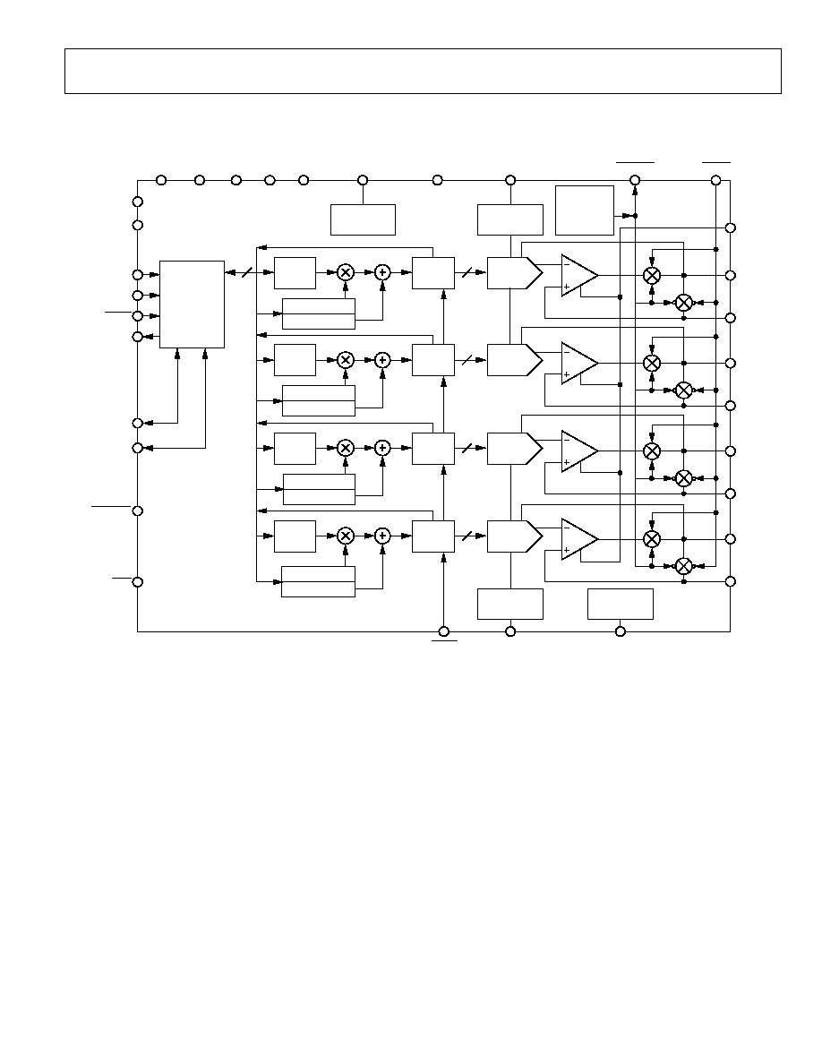
diagram, Figure 1.
i
CMOSTM
Process Technology
For analog systems designers within industrial/instrumentation equipment OEMs who need high performance ICs at higher-voltage levels, iCMOS is a
technology platform that enables the development of analog ICs capable of 30V and operating at +/-15V supplies while allowing dramatic reductions in
power consumption and package size, and increased AC and DC performance.
AD5744/AD5764

Preliminary Technical Data
Rev. PrA 15-Nov-04| Page 2 of 27
TABLE OF CONTENTS
Functional Block Diagram .............................................................. 3
Specifications..................................................................................... 4
AC Performance Characteristics ................................................ 6
Timing Characteristics ................................................................ 7
Absolute Maximum Ratings.......................................................... 10
ESD Caution................................................................................ 10
Pin Configuration and Function Descriptions........................... 11
Terminology .................................................................................... 13
typical performance characteristics ............................................. 15
General Description ....................................................................... 16
dac architecture........................................................................... 16
Reference Buffers........................................................................ 16
Serial interface ............................................................................ 16
Simultaneous Updating Via
LDAC
.......................................... 17
transfer function ......................................................................... 18
Asynchronous Clear (
CLR
)....................................................... 18
Function Register ....................................................................... 19
DAta register ............................................................................... 20
Coarse gain register.................................................................... 20
Fine gain register ........................................................................ 21
offset register............................................................................... 21
AD5744/64 Features....................................................................... 22
Analog Output Control ............................................................. 22
Digital Offset and Gain Control............................................... 22
Programmable Short-Circuit protection................................. 22
Digital I/O Port........................................................................... 22
Temperature Sensor ................................................................... 22
Local ground offset adjust......................................................... 22
applications information ............................................................... 23
typical operating circuit............................................................. 23
layout guidelines......................................................................... 24
Isolated interface ........................................................................ 24
microprocessor interfacing ....................................................... 24
Evaluation board ........................................................................ 26
Outline Dimensions ....................................................................... 27
Ordering Guide .......................................................................... 27
REVISION HISTORY
Revision PrA 15-Nov-04: Preliminary Version
AD5744/AD5764
Preliminary Technical Data
Rev. PrA 15-Nov-04| Page 3 of 27
FUNCTIONAL BLOCK DIAGRAM
INPUT
REG C
GAIN REG C
OFFSET REG C
DAC
REG C
14/16
DAC C
INPUT
REG D
GAIN REG D
REFERENCE
BUFFERS
OFFSET REG D
DAC
REG D
14/16
DAC D
G1
G2
INPUT
REG B
GAIN REG B
OFFSET REG B
DAC
REG B
14/16
DAC B
INPUT
REG A
GAIN REG A
OFFSET REG A
DAC
REG A
14/16
14/16
DAC A
LDAC
VREF CD
TEMP
RSTIN
RSTOUT
VREF AB
REFGND
AGNDD
VOUTD
AGNDC
VOUTC
AGNDB
VOUTB
AGNDA
VOUTA
ISCC
TEMP
SENSOR
REFERENCE
BUFFERS
AV
SS
SDIN
SCLK
SYNC
SDO
D0
D1
BIN/2SCOMP
CLR
AV
DD
AV
SS
AV
DD
PGND
DV
CC
DGND
+5V
REFERENCE
VOLTAGE
MONITOR
AND
CONTROL
INPUT SHIFT
REGISTER
AND
CONTROL
LOGIC
G1
G2
G1
G2
G1
G2
REFOUT
Figure 1. Functional Block Diagram
AD5744/AD5764

Preliminary Technical Data
Rev. PrA 15-Nov-04| Page 4 of 27
SPECIFICATIONS
AV
DD
= +11.4 V to +16.5 V, AV
SS
= -11.4 V to -16.5 V, AGND = DGND = REFGND = PGND=0 V; REFAB = REFCD= 5 V Ext;
DV
CC
= 2.7 V to 5.5 V, R
LOAD
= 10 k, C
L
= 200 pF. All specifications T
MIN
to T
MAX
, unless otherwise noted.
Table 1.
Parameter
A Grade
1
B
Grade
1
C
Grade
1
Unit
Test Conditions/Comments
ACCURACY
Resolution
16
14
16
14
16
14
Bits
AD5764
AD5744
Relative Accuracy (INL)
±4
±2
±1
LSB max
Differential Nonlinearity
±1
±1
±1
LSB max
Guaranteed monotonic
Bipolar Zero Error
±1
±1
±1
mV max
At 25°C. Error at other
temperatures
obtained using bipolar zero TC.
Bipolar Zero TC
±2
±2
±2
ppm FSR/°C max
Zero Code Error
±1
±1
±1
mV max
At 25°C. Error at other
temperatures
obtained using zero code TC.
Zero Code TC
±2
±2
±2
ppm FSR/°C max
Gain Error
±0.02
±0.02
±0.02
% FSR max
At 25°C. Error at other
temperatures
obtained using gain TC.
Gain TC
2
2
2
ppm FSR/°C max
DC Crosstalk
2
0.5
0.5
0.5
LSB max
REFERENCE INPUT/OUTPUT
Reference Input
2
Reference Input Voltage
5
5
5
V nom
±1% for specified performance
DC Input Impedance
1
1
1
M min
Typically 100 M
Input Current
±10
±10
±10
µA max
Typically ±30 nA
Reference Range
1/5
1/5
1/5
V min/max
Reference
Output
Output Voltage
4.999/5.001 4.999/5.001
4.999/5.001
V min/max
At 25°C
Reference TC
±10
±10
±10
ppm/°C max
Output Noise(0.1 Hz to 10 Hz)
TBD
TBD
TBD
µV p-p typ
Noise Spectral Density
TBD
TBD
TBD
nV/Hz typ
OUTPUT CHARACTERISTICS
2
Output Voltage Range
3
±10
±10
±10
V min/max
AV
DD
/AV
SS
= ±11.4 V
±13
±13
±13
V min/max
AV
DD
/AV
SS
= ±16.5 V
Output Voltage TC
±2
±2
±2
ppm FSR/°C max
Output Voltage Drift V
S
Time
±TBD
±TBD
±TBD
ppm FSR/1000 Hours
typ
Short Circuit Current
10
10
10
mA max
RI
SCC
= 6 K
, See Figure ???
Load Current
±1
±1
±1
mA max
For specified performance
Capacitive Load Stability
R
L
=
200
200
200
pF max
R
L
= 10 k
TBD
TBD
TBD
pF max
DC Output Impedance
0.3
0.3
0.3
max
DIGITAL INPUTS
2
DV
CC
= 2.7 V to 5.5 V, JEDEC
compliant
V
IH
, Input High Voltage
2
2
2
V min
1
Temperature range -40°C to +85°C; typical at +25°C. Device functionality is guaranteed to +105°C with degraded performance.
2
Guaranteed by characterization. Not production tested.
3
Output amplifier headroom requirement is 1.4 V min.
AD5744/AD5764
Preliminary Technical Data
Rev. PrA 15-Nov-04| Page 5 of 27
Parameter
A Grade
1
B
Grade
1
C
Grade
1
Unit
Test Conditions/Comments
V
IL
, Input Low Voltage
0.8
0.8
0.8
V max
Input Current
±10
±10
±10
µA max
Total for All Pins. T
A
= T
MIN
to T
MAX
.
Pin Capacitance
10
10
10
pF max
DIGITAL OUTPUTS (D0,D1, SDO)
2
Output Low Voltage
0.4
0.4
0.4
V max
DV
CC
= 5 V ± 10%, sinking 200 µA
Output High Voltage
DV
CC
1
DV
CC
1
DV
CC
1
V min
DV
CC
= 5 V ± 10%, Sourcing 200
µA
Output Low Voltage
0.4
0.4
0.4
V max
DV
CC
= 2.7 V to 3.6 V, Sinking 200
µA
Output High Voltage
DV
CC
0.5
DV
CC
0.5
DV
CC
0.5
V min
DV
CC
= 2.7 V to 3.6 V, Sourcing
200 µA
High Impedance Leakage
Current
±1
±1
±1
µA max
SDO only
High Impedance Output
Capacitance
5
5
5
pF typ
SDO only
TEMP
SENSOR
Accuracy
±1
±1
±1
°C typ
At 25°C
±5
±5
±5
°C max
-40°C < T <+85°C
Output Voltage @ 25°C
1.5
1.5
1.5
V typ
Output Voltage Scale Factor
5
5
5
mV/°C typ
Output Voltage Range
0/3.0
0/3.0
0/3.0
V min/max
Output Load Current
200
200
200
µA max
Current source only.
Power On Time
10
10
10
ms typ
To within ±5°C
POWER REQUIREMENTS
AV
DD
/AV
SS
11.4/16.5
11.4/16.5
11.4/16.5
V min/max
DV
CC
2.7/5.5
2.7/5.5
2.7/5.5
V min/max
Power Supply Sensitivity
4
V
OUT
/V
DD
-85
-85
-85
dB typ
AI
DD
3.75
3.75
3.75
mA/Channel max
Outputs unloaded
AI
SS
2.75
2.75
2.75
mA/Channel max
Outputs unloaded
DI
CC
1
1
1
mA max
V
IH
= DV
CC
, V
IL
= DGND. TBD mA
typ
Power Dissipation
244
244
244
mW typ
±12 V operation output
unloaded
4
Guaranteed by characterization. Not production tested.
AD5744/AD5764