 | ÐлекÑÑоннÑй компоненÑ: AD584U | СкаÑаÑÑ:  PDF PDF  ZIP ZIP |
/home/web/doc/html/ad/210868
REV. B
Information furnished by Analog Devices is believed to be accurate and
reliable. However, no responsibility is assumed by Analog Devices for its
use, nor for any infringements of patents or other rights of third parties that
may result from its use. No license is granted by implication or otherwise
under any patent or patent rights of Analog Devices.
a
AD584*
One Technology Way, P.O. Box 9106, Norwood, MA 02062-9106, U.S.A.
Tel: 781/329-4700
www.analog.com
Fax: 781/326-8703
© Analog Devices, Inc., 2001
Pin Programmable
Precision Voltage Reference
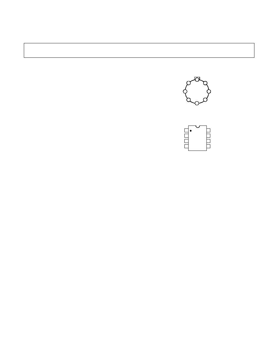
PIN CONFIGURATIONS
8-Lead TO-99
7
8
1
4
5
6
3
2
CAP
V
BG
STROBE
COMMON
TAB
10.0V
5.0V
2.5V
V+
AD584
TOP VIEW
(Not to Scale)
8-Lead DIP
TOP VIEW
(Not to Scale)
8
7
6
5
1
2
3
4
10.0V
5.0V
2.5V
+V
CAP
V
BG
STROBE
COMMON
AD584
FEATURES
Four Programmable Output Voltages:
10.000 V, 7.500 V, 5.000 V, 2.500 V
Laser-Trimmed to High Accuracies
No External Components Required
Trimmed Temperature Coefficient:
5 ppm/ C Max, 0 C to 70 C (AD584L)
15 ppm/ C Max, 55 C to +125 C (AD584T)
Zero Output Strobe Terminal Provided
Two Terminal Negative Reference
Capability (5 V and above)
Output Sources or Sinks Current
Low Quiescent Current: 1.0 mA Max
10 mA Current Output Capability
MIL-STD-883 Compliant Versions Available
GENERAL DESCRIPTION
The AD584 is an eight-terminal precision voltage reference offer-
ing pin-programmable selection of four popular output voltages:
10.000 V, 7.500 V, 5.000 V and 2.500 V. Other output voltages,
above, below or between the four standard outputs, are available
by the addition of external resistors. Input voltage may vary between
4.5 V and 30 V.
Laser Wafer Trimming (LWT) is used to adjust the pin-
programmable output levels and temperature coefficients,
resulting in the most flexible high precision voltage reference
available in monolithic form.
In addition to the programmable output voltages, the AD584 offers
a unique strobe terminal which permits the device to be turned
on or off. When the AD584 is used as a power supply reference,
the supply can be switched off with a single, low-power signal.
In the "off" state the current drain by the AD584 is reduced to
about 100
µA. In the "on" state the total supply current is typi-
cally 750
µA including the output buffer amplifier.
The AD584 is recommended for use as a reference for 8-, 10-,
or 12-bit D/A converters which require an external precision
reference. The device is also ideal for all types of A/D convert-
ers of up to 14-bit accuracy, either successive approximation or
integrating designs, and in general can offer better performance
than that provided by standard self-contained references.
The AD584J, K, and L are specified for operation from 0
°C to
70
°C; the AD584S and T are specified for the 55°C to +125°C
range. All grades are packaged in a hermetically sealed eight-
terminal TO-99 metal can; the AD584 J and K are also available
in an 8-lead plastic DIP.
PRODUCT HIGHLIGHTS
1. The flexibility of the AD584 eliminates the need to design-in
and inventory several different voltage references. Further
more one AD584 can serve as several references simultaneously
when buffered properly.
2. Laser trimming of both initial accuracy and temperature coeffi-
cient results in very low errors over temperature without the
use of external components. The AD584LH has a maximum
deviation from 10.000 V of
±7.25 mV from 0°C to 70°C.
3. The AD584 can be operated in a two-terminal "Zener" mode
at 5 V output and above. By connecting the input and the
output, the AD584 can be used in this "Zener" configuration
as a negative reference.
4. The output of the AD584 is configured to sink or source
currents. This means that small reverse currents can be toler-
ated in circuits using the AD584 without damage to the refer-
ence and without disturbing the output voltage (10 V, 7.5 V,
and 5 V outputs).
5. The AD584 is available in versions compliant with MIL-STD-
883. Refer to the Analog Devices Military Products Databook
or current AD584/883B data sheet for detailed specifications.
*Protected by U.S. Patent No. 3,887,863; RE 30,586.

REV. B
2
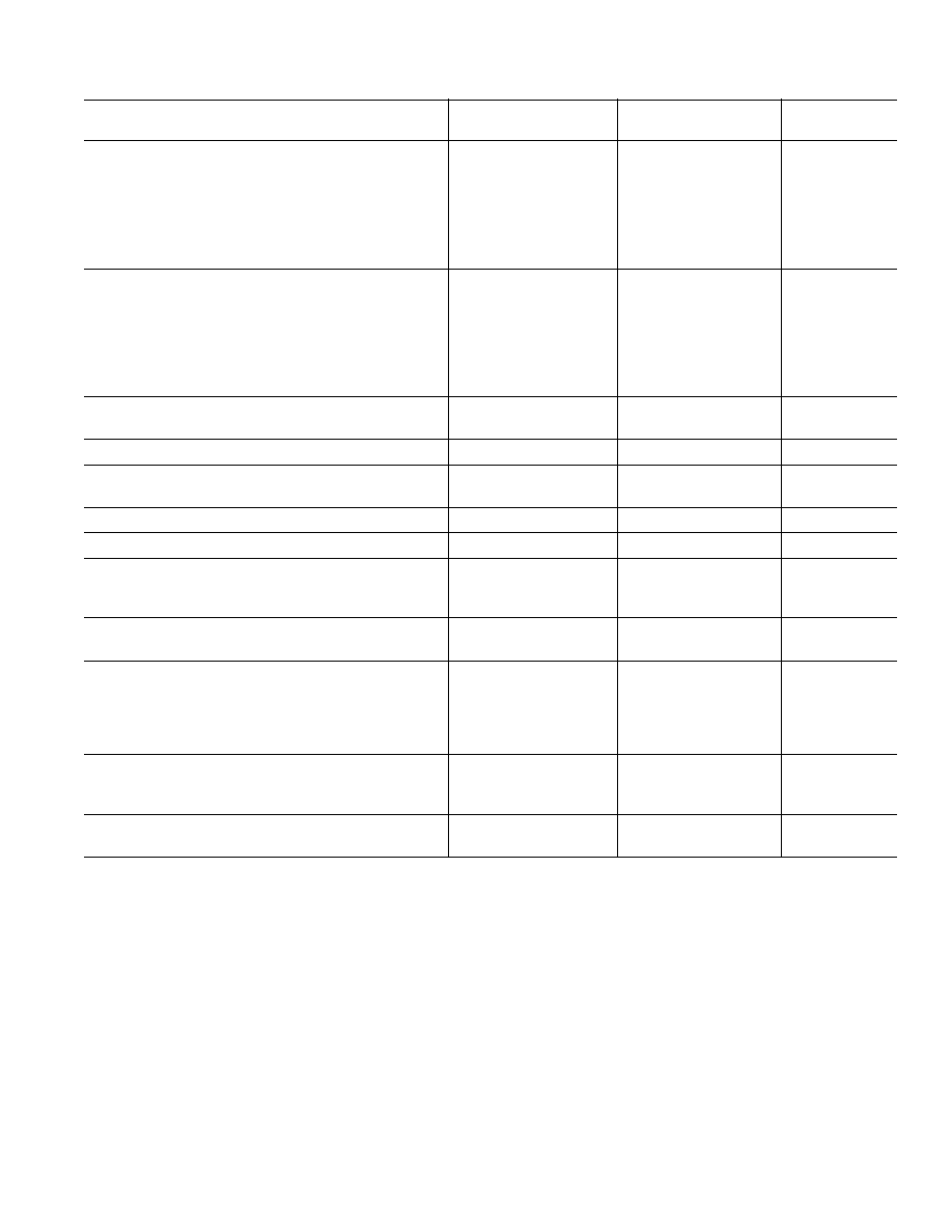
AD584SPECIFICATIONS
(@ V
IN
= 15 V and 25 C unless otherwise noted.)
Model
AD584J
AD584K
AD584L
Min
Typ
Max
Min
Typ
Max
Min
Typ
Max
Unit
OUTPUT VOLTAGE TOLERANCE
Maximum Error
1
for Nominal
Outputs of:
10.000 V
30
10
5
mV
7.500 V
20
8
4
mV
5.000 V
15
6
3
mV
2.500 V
7.5
3.5
2.5
mV
OUTPUT VOLTAGE CHANGE
Maximum Deviation from 25
°C
Value, T
MIN
to T
MAX
2
10.000 V, 7.500 V, 5.000 V Outputs
30
15
5
ppm/
°C
2.500 V Output
30
15
10
ppm/
°C
Differential Temperature
Coefficients Between Outputs
5
3
3
ppm/
°C
QUIESCENT CURRENT
0.75
1.0
0.75
1.0
0.75
1.0
mA
Temperature Variation
1.5
1.5
1.5
µA/°C
TURN-ON SETTLING TIME TO 0.1%
200
200
200
µs
NOISE
(0.1 Hz to 10 Hz)
50
50
50
µV p-p
LONG-TERM STABILITY
25
25
25
ppm/1000 Hrs
SHORT-CIRCUIT CURRENT
30
30
30
mA
LINE REGULATION (No Load)
15 V
V
IN
30 V
0.002
0.002
0.002
%/V
(V
OUT
2.5 V)
V
IN
15 V
0.005
0.005
0.005
%/V
LOAD REGULATION
0
I
OUT
5 mA, All Outputs
20
50
20
50
20
50
ppm/mA
OUTPUT CURRENT
V
IN
V
OUT
2.5 V
Source @ 25
°C
10
10
10
mA
Source T
MIN
to T
MAX
5
5
5
mA
Sink T
MIN
to T
MAX
5
5
5
mA
TEMPERATURE RANGE
Operating
0
70
0
70
0
70
°C
Storage
65
+175
65
+175
65
+175
°C
PACKAGE OPTION
3
TO-99 (H-08A)
AD584JH
AD584KH
AD584LH
Plastic (N-8)
AD584JN
AD584KN
NOTES
1
At Pin 1.
2
Calculated as average over the operating temperature range.
3
H = Hermetic Metal Can; N = Plastic DIP.
Specifications subject to change without notice.
Specifications shown in boldface are tested on all production units at final electrical
test. Results from those tests are used to calculate outgoing quality levels. All min
and max specifications are guaranteed, although only those shown in boldface are
tested on all production units.
REV. B
3
AD584
Model
AD584S
AD584T
Min
Typ
Max
Min
Typ
Max
Unit
OUTPUT VOLTAGE TOLERANCE
Maximum Error
1
for Nominal
Outputs of:
10.000 V
30
10
mV
7.500 V
20
8
mV
5.000 V
15
±
6
mV
2.500 V
7.5
3.5
mV
OUTPUT VOLTAGE CHANGE
Maximum Deviation from 25
°C
Value, T
MIN
to T
MAX
2
10.000 V, 7.500 V, 5.000 V Outputs
30
15
ppm/
°C
2.500 V Output
30
20
ppm/
°C
Differential Temperature
Coefficients Between Outputs
5
3
ppm/
°C
QUIESCENT CURRENT
0.75
1.0
0.75
1.0
mA
Temperature Variation
1.5
1.5
µA/°C
TURN-ON SETTLING TIME TO 0.1%
200
200
µs
NOISE
(0.1 Hz to 10 Hz)
50
50
µV p-p
LONG-TERM STABILITY
25
25
ppm/1000 Hrs
SHORT-CIRCUIT CURRENT
30
30
mA
LINE REGULATION (No Load)
15 V
V
IN
30 V
0.002
0.002
%/V
(V
OUT
2.5 V)
V
IN
15 V
0.005
0.005
%/V
LOAD REGULATION
0
I
OUT
5 mA, All Outputs
20
50
20
50
ppm/mA
OUTPUT CURRENT
V
IN
V
OUT
2.5 V
Source @ 25
°C
10
10
mA
Source T
MIN
to T
MAX
5
5
mA
Sink T
MIN
to T
MAX
5
5
mA
TEMPERATURE RANGE
Operating
55
+125
55
+125
°C
Storage
65
+175
65
+175
°C
PACKAGE OPTION
TO-99 (H-08A)
AD584SH
AD584TH
NOTES
1
At Pin 1.
2
Calculated as average over the operating temperature range.
Specifications subject to change without notice.
Specifications shown in boldface are tested on all production units at final electrical
test. Results from those tests are used to calculate outgoing quality levels. All min
and max specifications are guaranteed, although only those shown in boldface are
tested on all production units.
REV. B
AD584
4
CAUTION
ESD (electrostatic discharge) sensitive device. Electrostatic charges as high as 4000 V readily
accumulate on the human body and test equipment and can discharge without detection. Although
the AD584 features proprietary ESD protection circuitry, permanent damage may occur on devices
subjected to high-energy electrostatic discharges. Therefore, proper ESD precautions are
recommended to avoid performance degradation or loss of functionality.
WARNING!
ESD SENSITIVE DEVICE
ABSOLUTE MAXIMUM RATINGS
Input Voltage V
IN
to Ground . . . . . . . . . . . . . . . . . . . . . . 40 V
Power Dissipation
@ 25
°C . . . . . . . . . . . . . . . . . . . . . 600 mW
Operating Junction Temperature Range . . . 55
°C to +125°C
Lead Temperature (Soldering 10 sec) . . . . . . . . . . . . . . 300
°C
Thermal Resistance
Junction-to-Ambient (H-08A) . . . . . . . . . . . . . . . 150
°C/W
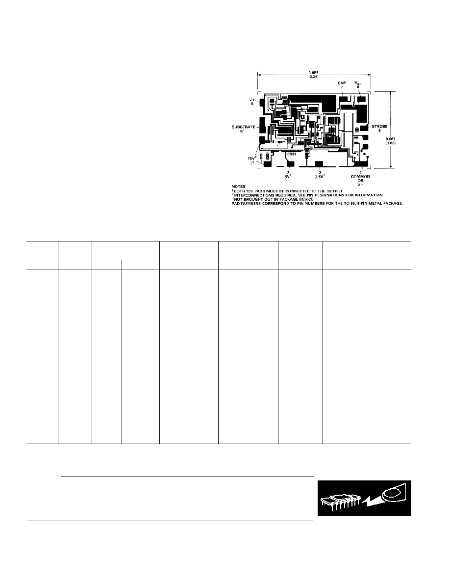
METALIZATION PHOTOGRAPH
Dimensions shown in inches and (mm).
ORDERING GUIDE
Ouput
Temperature
No. of
Temperature
Voltage
Initial Accuracy
Coefficient
Package
Package
Parts per
Range
Model
V
O
mV
%
ppm/ C
Description
Option
Package
C
AD584L
2.5
±2.5
0.10
10
TO-99
H-8
100
0 to 70
AD584K
2.5
±3.5
0.14
15
TO-99, Plastic
H-8, N-8
100, 48
0 to 70
AD584T
2.5
±3.5
0.14
20
TO-99
H-8
100
55 to +125
AD584S
2.5
±7.5
0.30
30
TO-99
H-8
100
55 to +125
AD584J
2.5
±7.5
0.30
30
TO-99, Plastic
H-8, N-8
100, 48
0 to 70
AD584L
5
±3
0.06
5
TO-99
H-8
100
0 to 70
AD584K
5
±6
0.12
15
TO-99, Plastic
H-8, N-8
100, 48
0 to 70
AD584T
5
±6
0.12
15
TO-99
H-8
100
55 to +125
AD584S
5
±15
0.30
30
TO-99
H-8
48
55 to +125
AD584J
5
±15
0.30
30
TO-99, Plastic
H-8, N-8
100, 48
0 to 70
AD584L
7.50
±4
0.05
5
TO-99
H-8
100
0 to 70
AD584K
7.50
±8
0.11
15
TO-99, Plastic
H-8, N-8
100, 48
0 to 70
AD584T
7.50
±8
0.11
15
TO-99
H-8
100
55 to +125
AD584S
7.50
±20
0.27
30
TO-99
H-8
100
55 to +125
AD584J
7.50
±20
0.27
30
TO-99, Plastic
H-8, N-8
100, 48
0 to 70
AD584L
10.00
±5
0.05
5
TO-99
H-8
100
0 to 70
AD584K
10.00
±10
0.10
15
TO-99, Plastic
H-8, N-8
100, 48
0 to 70
AD584T
10.00
±10
0.10
15
TO-99
H-8
100
55 to +125
AD584S
10.00
±30
0.30
30
TO-99
H-8
100
55 to +125
AD584J
10.00
±30
0.30
30
TO-99, Plastic
H-8, N-8
100, 48
0 to 70
REV. B
AD584
5
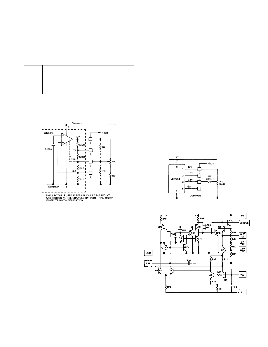
APPLYING THE AD584
With power applied to Pins 8 and 4 and all other pins open, the
AD584 will produce a buffered nominal 10.0 V output between
Pins 1 and 4 (see Figure 1). The stabilized output voltage may be
reduced to 7.5 V, 5.0 V, or 2.5 V by connecting the program-
ming pins as follows:
Output
Voltage
Pin Programming
7.5 V
Join the 2.5 V and 5.0 V pins (2) and (3).
5.0 V
Connect the 5.0 V pin (2) to the output pin (1).
2.5 V
Connect the 2.5 V pin (3) to the output pin (1).
The options shown above are available without the use of any addi-
tional components. Multiple outputs using only one AD584, are
also possible by simply buffering each voltage programming pin
with a unity-gain noninverting op amp.
Figure 1. Variable Output Options
The AD584 can also be programmed over a wide range of output
voltages, including voltages greater than 10 V, by the addition of
one or more external resistors. Figure 1 illustrates the general adjust-
ment procedure, with approximate values given for the internal
resistors of the AD584. The AD584 may be modeled as an op amp
with a noninverting feedback connection, driven by a high stability
1.215 V bandgap reference (see Figure 3 for schematic).
When the feedback ratio is adjusted with external resistors, the
output amplifier can be made to multiply the reference voltage by
almost any convenient amount, making popular outputs of 10.24 V,
5.12 V, 2.56 V, or 6.3 V easy to obtain. The most general adjust-
ment (which gives the greatest range and poorest resolution) uses
R1 and R2 alone (see Figure 1). As R1 is adjusted to its upper limit
the 2.5 V Pin 3 will be connected to the output, which will reduce
to 2.5 V. As R1 is adjusted to its lower limit, the output voltage
will rise to a value limited by R2. For example, if R2 is about 6 k
,
the upper limit of the output range will be about 20 V even for large
values of R1. R2 should not be omitted; its value should be chosen
to limit the output to a value which can be tolerated by the load
circuits. If R2 is zero, adjusting R1 to its lower limit will result in a
loss of control over the output voltage. If precision voltages are
required to be set at levels other than the standard outputs, the
20% absolute tolerance in the internal resistor ladder must be
accounted for.
Alternatively, the output voltage can be raised by loading the 2.5 V
tap with R3 alone. The output voltage can be lowered by connect-
ing R4 alone. Either of these resistors can be a fixed resistor selected
by test or an adjustable resistor. In all cases the resistors should
have a low temperature coefficient to match the AD584 internal
resistors, which have a negative TC less than 60 ppm/
°C. If both
R3 and R4 are used, these resistors should have matched tempera-
ture coefficients.
When only small adjustments or trims are required, the circuit of
Figure 2 offers better resolution over a limited trim range. The
circuit can be programmed to 5.0 V, 7.5 V, or 10 V and adjusted
by means of R1 over a range of about
±200 mV. To trim the 2.5 V
output option, R2 (Figure 2) can be reconnected to the bandgap
reference (Pin 6). In this configuration, the adjustment should be
limited to
±100 mV in order to avoid affecting the performance of
the AD584.
Figure 2. Output Trimming
Figure 3. Schematic Diagram