 | ÐлекÑÑоннÑй компоненÑ: AD587K | СкаÑаÑÑ:  PDF PDF  ZIP ZIP |
AD587 Data Sheet
FUNCTIONAL BLOCK DIAGRAM
8
2
6
4
5
R
T
R
F
R
I
R
S
AD587
A1
+V
I N
NOISE
REDUCTION
V
OUT
TRIM
GND
NOTE:
PINS 1,3, AND 7 ARE INTERNAL TEST POINTS.
NO CONNECTIONS TO THESE POINTS.
REV. D
Information furnished by Analog Devices is believed to be accurate and
reliable. However, no responsibility is assumed by Analog Devices for its
use, nor for any infringements of patents or other rights of third parties
which may result from its use. No license is granted by implication or
otherwise under any patent or patent rights of Analog Devices.
a
High Precision
10 V Reference
AD587
FEATURES
Laser Trimmed to High Accuracy:
10.000 V 5 mV (L and U Grades)
Trimmed Temperature Coefficient:
5 ppm/ C max, (L and U Grades)
Noise Reduction Capability
Low Quiescent Current: 4 mA max
Output Trim Capability
MIL-STD-883 Compliant Versions Available
PRODUCT HIGHLIGHTS
1. Laser trimming of both initial accuracy and temperature
coefficients results in very low errors over temperature with-
out the use of external components. The AD587L has a
maximum deviation from 10.000 V of
±
8.5 mV between 0
°
C
and +70
°
C, and the AD587U guarantees
±
14 mV maximum
total error between 55
°
C and +125
°
C.
2. For applications requiring higher precision, an optional fine
trim connection is provided.
3. Any system using an industry standard pinout 10 volt refer-
ence can be upgraded instantly with the AD587.
4. Output noise of the AD587 is very low, typically 4
µ
V p-p. A
noise reduction pin is provided for additional noise filtering
using an external capacitor.
5. The AD587 is available in versions compliant with MIL-
STD-883. Refer to the Analog Devices Military Products
Databook or current AD587/883B data sheet for detailed
specifications.
PRODUCT DESCRIPTION
The AD587 represents a major advance in the state-of-the-art in
monolithic voltage references. Using a proprietary ion-implanted
buried Zener diode and laser wafer trimming of high stability
thin-film resistors, the AD587 provides outstanding perfor-
mance at low cost.
The AD587 offers much higher performance than most other
10 V references. Because the AD587 uses an industry standard
pinout, many systems can be upgraded instantly with the
AD587. The buried Zener approach to reference design pro-
vides lower noise and drift than bandgap voltage references. The
AD587 offers a noise reduction pin which can be used to further
reduce the noise level generated by the buried Zener.
The AD587 is recommended for use as a reference for 8-, 10-,
12-, 14- or 16-bit D/A converters which require an external
precision reference. The device is also ideal for successive
approximation or integrating A/D converters with up to 14 bits
of accuracy and, in general, can offer better performance than
the standard on-chip references.
The AD587J, K and L are specified for operation from 0
°
C to
+70
°
C, and the AD587S, T and U are specified for 55
°
C to
+125
°
C operation. All grades are available in 8-pin cerdip. The
J and K versions are also available in an 8-pin Small Outline IC
(SOIC) package for surface mount applications, while the J, K,
and L grades also come in an 8-pin plastic package.
One Technology Way, P.O. Box 9106, Norwood, MA 02062-9106, U.S.A.
Tel: 781/329-4700
World Wide Web Site: http://www.analog.com
Fax: 781/326-8703
© Analog Devices, Inc., 2000
AD587SPECIFICATIONS
Model
AD587J/S
AD587K/T
AD587L/U
Min
Typ
Max
Min
Typ
Max
Min
Typ
Max
Units
OUTPUT VOLTAGE
9.990
10.010
9.995
10.005
9.995
10.005
V
OUTPUT VOLTAGE DRIFT
1
0
°
C to +70
°
C
20
10
5
ppm/
°
C
55
°
C to +125
°
C
20
10
5
GAIN ADJUSTMENT
+3
+3
+3
%
1
1
1
LINE REGULATION
1
13.5 V
+ V
IN
36 V
T
MIN
to T
MAX
100
100
100
±µ
V/V
LOAD REGULATION
1
Sourcing 0 < I
OUT
< 10 mA
T
MIN
to T
MAX
100
100
100
±µ
V/mA
Sourcing 10 < I
OUT
< 0 mA
2
T
MIN
to T
MAX
100
100
100
QUIESCENT CURRENT
2
4
2
4
2
4
mA
POWER DISSIPATION
30
30
30
mW
OUTPUT NOISE
0.1 Hz to 10 Hz
4
4
4
µ
V p-p
Spectral Density, 100 Hz
100
100
100
nV/
Hz
LONG-TERM STABILITY
15
15
15
±
ppm/1000 Hr.
SHORT-CIRCUIT CURRENT-TO-GROUND
30
70
30
70
30
70
mA
SHORT-CIRCUIT CURRENT-TO-V
IN
30
70
30
70
30
70
mA
TEMPERATURE RANGE
Specified Performance (J, K, L)
0
+70
0
+70
0
+70
°
C
Operating Performance (J, K, L)
3
40
+85
40
+85
40
+85
Specified Performance (S, T, U)
55
+125
55
+125
55
+125
Operating Performance (S, T, U)
3
55
+125
55
+125
55
+125
NOTES
1
Spec is guaranteed for all packages and grades. Cerdip packaged parts are 100% production test.
2
Load Regulation (Sinking) specification for SOIC (R) package is
±
200
µ
V/mA.
3
The operating temperature ranged is defined as the temperatures extremes at which the device will still function. Parts may deviate from their specified performance
outside their specified temperature range.
Specifications subject to change without notice.
(T
A
= +25 C, V
IN
= +15 V unless otherwise noted)
ORDERING GUIDE
Initial
Temperature
Temperature
Package
Model
1
Error
Coefficient
Range
Options
2
AD587JQ
10 mV
20 ppm/
°
C
0
°
C to +70
°
C
Q-8
AD587JR
10 mV
20 ppm/
°
C
0
°
C to +70
°
C
SO-8
AD587JN
10 mV
20 ppm/
°
C
0
°
C to +70
°
C
N-8
AD587KQ
5 mV
10 ppm/
°
C
0
°
C to +70
°
C
Q-8
AD587KR
5 mV
10 ppm/
°
C
0
°
C to +70
°
C
SO-8
AD587KN
5 mV
10 ppm/
°
C
0
°
C to +70
°
C
N-8
AD587LQ
5 mV
5 ppm/
°
C
0
°
C to +70
°
C
Q-8
AD587LN
5 mV
5 ppm/
°
C
0
°
C to +70
°
C
N-8
AD587SQ
10 mV
20 ppm/
°
C
55
°
C to +125
°
C
Q-8
AD587TQ
10 mV
10 ppm/
°
C
55
°
C to +125
°
C
Q-8
AD587UQ
5 mV
5 ppm/
°
C
55
°
C to +125
°
C
Q-8
AD587JCHIPS
10 mV
20 ppm/
°
C
0
°
C to +70
°
C
NOTES
1
For details on grade and package offerings screened in accordance with MIL-STD-883, refer to the
Analog Devices Military Products Databook or current AD587/883B data sheet.
2
N = Plastic DIP; Q = Cerdip; SO = SOIC.
REV. D
2
AD587
REV. D
3
ABSOLUTE MAXIMUM RATINGS*
V
IN
to Ground . . . . . . . . . . . . . . . . . . . . . . . . . . . . . . . . . . 36 V
Power Dissipation (+25
°
C) . . . . . . . . . . . . . . . . . . . . . 500 mW
Storage Temperature . . . . . . . . . . . . . . . . . . . 65
°
C to +150
°
C
Lead Temperature (Soldering, 10 sec) . . . . . . . . . . . . +300
°
C
Package Thermal Resistance
JC
. . . . . . . . . . . . . . . . . . . . . . . . . . . . . . . . . . . . . . 22
°
C/W
JA
. . . . . . . . . . . . . . . . . . . . . . . . . . . . . . . . . . . . . 110
°
C/W
Output Protection: Output safe for indefinite short to ground and
momentary short to V
IN
.
*Stresses above those listed under Absolute Maximum Ratings may cause perma-
nent damage to the device. This is a stress rating only; functional operation of the
device at these or any other conditions above those indicated in the operational
sections of this specification is not implied. Exposure to absolute maximum rating
conditions for extended periods may affect device reliability.
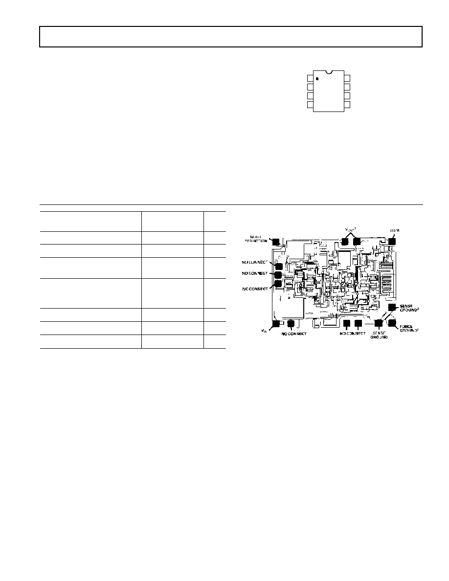
DIE SPECIFICATIONS
The following specifications are tested at the die level for AD587JCHIPS. These die are probed at +25
°
C only.
(T
A
= +25
°
C, V
IN
= +15 V unless otherwise noted)
AD587JCHIPS
Parameter
Min
Typ
Max
Units
Output Voltage
9.990
10.010 V
Gain Adjustment
1
3
%
Line Regulation
13.5 V < + V
IN
< 36 V
100
±µ
V/V
Load Regulation
Sourcing 0 < I
OUT
< 10 mA
100
µ
V/mA
Sinking 10 < I
OUT
< 0 mA
100
µ
V/mA
Quiescent Current
2
4
mA
Short-Circuit Current-to-Ground
70
mA
Short-Circuit Currrent-to-V
OUT
70
mA
NOTES
1
Both V
OUT
pads should be connected to the output.
2
Sense and force grounds must be tied together.
Die Thickness: The standard thickness of Analog Devices Bipolar dice is 24 mils
±
2 mils.
Die Dimensions: The dimensions given have a tolerance of
±
2 mils.
Backing: The standard backside surface is silicon (not plated). Analog Devices does not recommend
gold-backed dice for most applications.
Edges: A diamond saw is used to separate wafers into dice thus providing perpendicular edges half-
way through the die.
In contrast to scribed dice, this technique provides a more uniform die shape and size . The perpen-
dicular edges facilitate handling (such as tweezer pick-up) while the uniform shape and size simplifies
substrate design and die attach.
Top Surface: The standard top surface of the die is covered by a layer of glassivation . All areas are
covered except bonding pads and scribe lines.
Surface Metalization: The metalization to Analog Devices bipolar dice is aluminum. Minimum
thickness is 10,000Å.
Bonding Pads: All bonding pads have a minimum size of 4 mils by 4 mils. The passivation windows
have 3.5 mils by 3.5 mils minimum.
DIE LAYOUT
PIN CONFIGURATION
1
2
3
4
8
7
6
5
TOP VIEW
(Not to Scale)
AD587
TP
*
TRIM
V
OUT
TP
*
NOISE
REDUCTION
+V
I N
TP
*
GND
*
TP DENOTES FACTORY TEST POINT.
NO CONNECTIONS SHOULD BE MADE
TO THESE PINS.
Die Size: 0.081
×
0.060 Inches
AD587
REV. D
4
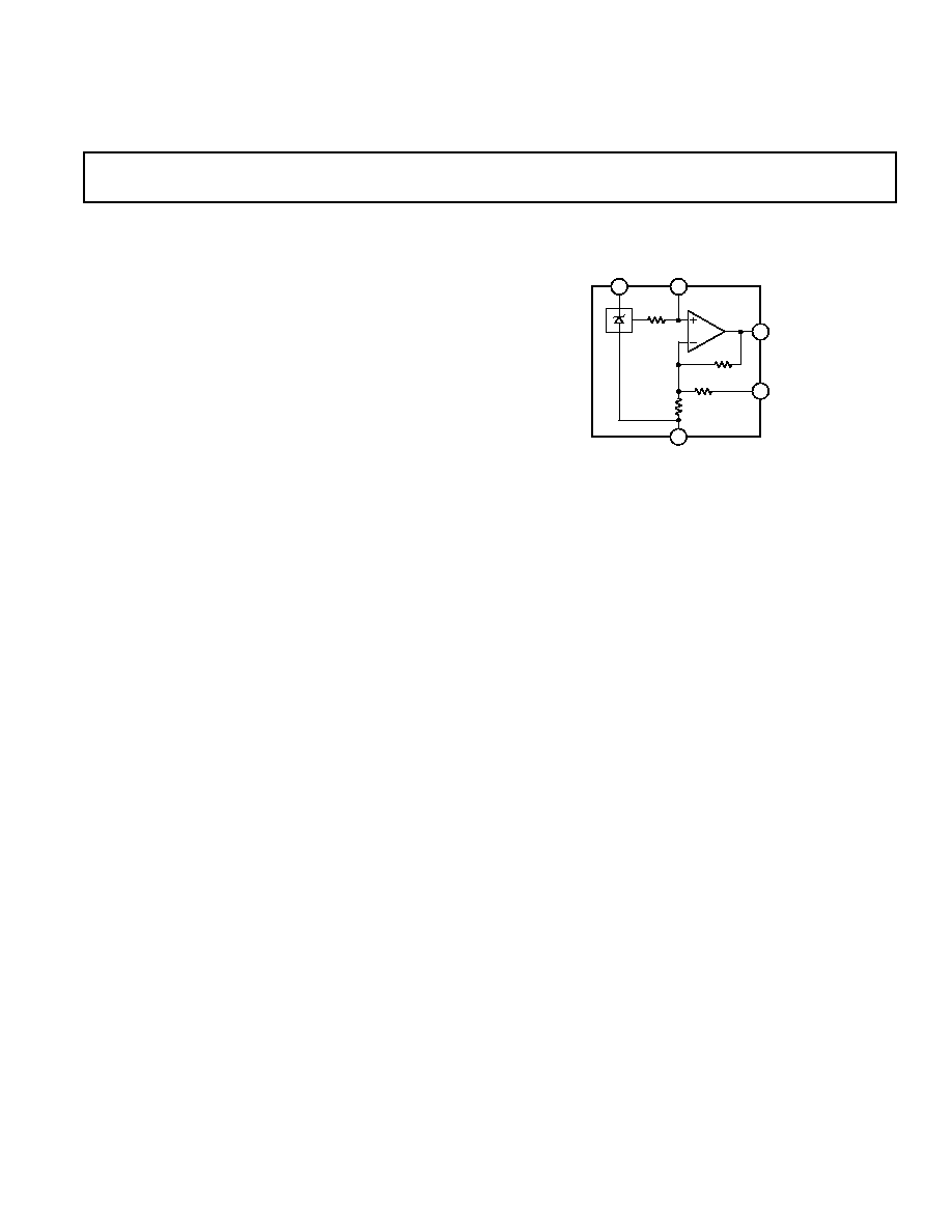
THEORY OF OPERATION
The AD587 consists of a proprietary buried Zener diode refer-
ence, an amplifier to buffer the output and several high stability
thin-film resistors as shown in the block diagram in Figure 1.
This design results in a high precision monolithic 10 V output
reference with initial offset of 5 mV or less. The temperature
compensation circuitry provides the device with a temperature
coefficient of under 5 ppm/
°
C.
8
2
6
4
5
R
T
R
F
R
I
R
S
AD587
A1
+V
I N
NOISE
REDUCTION
V
OUT
TRIM
GND
NOTE:
PINS 1,3, AND 7 ARE INTERNAL TEST POINTS.
NO CONNECTIONS TO THESE POINTS.
Figure 1. AD587 Functional Block Diagram
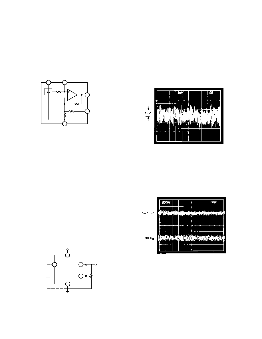
A capacitor can be added at the NOISE REDUCTION pin (Pin
8) to form a low-pass filter with R
S
to reduce the noise contribu-
tion of the Zener to the circuit.
APPLYING THE AD587
The AD587 is simple to use in virtually all precision reference
applications. When power is applied to Pin 2, and Pin 4 is
grounded, Pin 6 provides a 10 V output. No external compo-
nents are required; the degree of desired absolute accuracy is
achieved simply by selecting the required device grade. The
AD587 requires less than 4 mA quiescent current from an oper-
ating supply of +15 V.
Fine trimming may be desired to set the output level to exactly
10.000 V (calibrated to a main system reference). System cali-
bration may also require a reference voltage that is slightly differ-
ent from 10.000 V, for example, 10.24 V for binary applications.
In either case, the optional trim circuit shown in Figure 2 can
offset the output by as much as 300 mV, if desired, with mini-
mal effect on other device characteristics.
8
2
6
4
GND
5
AD587
V
I N
NOISE
REDUCTION
TRIM
V
O
10k
OUTPUT
+V
I N
C
N
1µF
OPTIONAL
NOISE
REDUCTION
CAPACITOR
Figure 2. Optional Fine Trim Configuration
NOISE PERFORMANCE AND REDUCTION
The noise generated by the AD587 is typically less than 4
µ
V
p-p over the 0.1 Hz to 10 Hz band. Noise in a 1 MHz band-
width is approximately 200
µ
V p-p. The dominant source of
this noise is the buried Zener which contributes approximately
100 nV/
Hz. In comparison, the op amp's contribution is negli-
gible. Figure 3 shows the 0.1 Hz to 10 Hz noise of a typical
AD587. The noise measurement is made with a bandpass filter
made of a 1-pole high-pass filter with a corner frequency at
0.1 Hz and a 2-pole low-pass filter with a corner frequency at
12.6 Hz to create a filter with a 9.922 Hz bandwidth.
Figure 3. 0.1 Hz to 10 Hz Noise
If further noise reduction is desired, an external capacitor may
be added between the NOISE REDUCTION pin and ground as
shown in Figure 2. This capacitor, combined with the 4 k
R
S
and the Zener resistances, form a low-pass filter on the output
of the Zener cell. A 1
µ
F capacitor will have a 3 dB point at
40 Hz, and it will reduce the high frequency (to 1 MHz) noise
to about 160
µ
V p-p. Figure 4 shows the 1 MHz noise of a typi-
cal AD587 both with and without a 1
µ
F capacitor.
Figure 4. Effect of 1
µ
F Noise Reduction Capacitor on
Broadband Noise
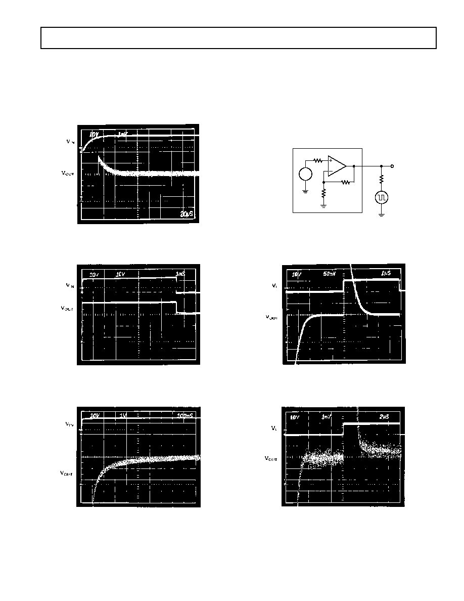
TURN-ON TIME
Upon application of power (cold start), the time required for the
output voltage to reach its final value within a specified error
band is defined as the turn-on settling time. Two components
normally associated with this are: the time for the active circuits
to settle, and the time for the thermal gradients on the chip to
stabilize. Figure 5 shows the turn-on characteristics of the
AD587. It shows the settling to be about 60
µ
s to 0.01%. Note
the absence of any thermal tails when the horizontal scale is ex-
panded to 1 ms/cm in Figure 5b.
AD587
REV. D
5
DYNAMIC PERFORMANCE
The output buffer amplifier is designed to provide the AD587
with static and dynamic load regulation superior to less com-
plete references.
Many A/D and D/A converters present transient current loads
to the reference, and poor reference response can degrade the
converter's performance.
Figure 6 displays the characteristics of the AD587 output ampli-
fier driving a 0 mA to 10 mA load.
Output turn-on time is modified when an external noise reduc-
tion capacitor is used. When present, this capacitor acts as an
additional load to the internal Zener diode's current source, re-
sulting in a somewhat longer turn-on time. In the case of a 1
µ
F
capacitor, the initial turn-on time is approximately 400 ms to
0.01% (see Figure 5c).
a. Electrical Turn-On
b. Extended Time Scale
c. Turn-On with 1
µ
F C
N
Figure 5. Turn-On Characteristics
Figure 6a. Transient Load Test Circuit
Figure 6b. Large-Scale Transient Response
Figure 6c. Fine Scale Settling for Transient Load
AD587
V
OUT
7.0V
1k
V
L
10V
0V