 | ÐлекÑÑоннÑй компоненÑ: AD5932 | СкаÑаÑÑ:  PDF PDF  ZIP ZIP |
AD5932 Programmable Single-Scan Waveform Generator Preliminary Data Sheet (REV. PrA)
Programmable Single-Scan
Waveform Generator
Preliminary Technical Data
AD5932*
Rev. PrA 02/05
Information furnished by Analog Devices is believed to be accurate and reliable.
However, no responsibility is assumed by Analog Devices for its use, nor for any
infringements of patents or other rights of third parties that may result from its use.
Specifications subject to change without notice. No license is granted by implication
or otherwise under any patent or patent rights of Analog Devices. Trademarks and
registered trademarks are the property of their respective owners.
One Technology Way, P.O. Box 9106, Norwood, MA 02062-9106, U.S.A.
Tel: 781.329.4700
www.analog.com
Fax: 781.326.8703
© 2005 Analog Devices, Inc. All rights reserved.
FEATURES
Programmable frequency profile--no external components
necessary
Ouput frequency up to 25 Mhz
Predefined frequency profile minimizes number of
DSP/µcontroller writes
Sinusoidal/triangular/square wave outputs
Powerdown mode (20 µA)
+2.3 V to +5.5 V power supply
Extended temperature range -40°C to +105°C
16-pin TSSOP
APPLICATIONS
Frequency Scan
Network/Impedance Measurements
Incremental Frequency stimulus
Sensory Applications--Proximity and Motion
BFSK
GENERAL DESCRIPTION
The AD5932 is a waveform generator providing a
programmable frequency scan. Utilizing embedded digital
processing allowing enhanced frequency control the device
generates synthesized analog or digital frequency-stepped
waveforms. Because frequency profiles are preprogrammed
continuous write cycles are eliminated, thereby freeing up
valuable DSP/µController resources. Waveforms start from a
known phase and are incremented phase continuously allowing
phase shifts to be easily determined. Consuming only 8mA the
AD5932 provides a convenient low power solution to waveform
generation.
To program the device, the user enters the start frequency, the
increment step size, the number of increments to be made and
the time interval the part stays at each frequency. The frequency
profile can be initiated by toggling the CTRL pin.
(continued on Page 3)
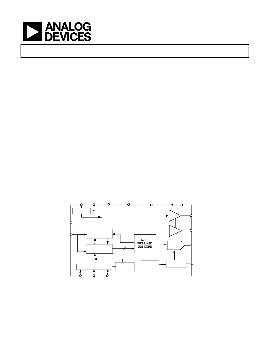
FUNCTIONAL BLOCK DIAGRAM
FREQUENCY
CONTROLLER
10-BIT
DAC
MCLK
CTRL
VOUT
FSYNC
SCLK
SDATA
SERIAL INTERFACE
SYNC OUT
MSB OUT
INCREMENT
CONTROLLER
ON-BOARD
REFERENCE
FULL-SCALE
CONTROL
COMP
CONTROL
REGISTER
DATA
DATA
CAP/2.5V
DVDD
VCC
2.5V
REGULATOR
24
INCR
BUFFER
BUFFER
SYNC
DGND
INTERUPT
STANDBY
AVDD
AGND
& CONTROL
Figure 1.
*Protected by US Patent Number 6747583, other patents pending

AD5932
Preliminary Technical Data
Rev. PrA | Page 2 of 15
TABLE OF CONTENTS
General Description ......................................................................... 3
Specifications..................................................................................... 4
Absolute Maximum Ratings............................................................ 6
ESD Caution.................................................................................. 6
Pin Configurations And Functional Descriptions ....................... 7
Terminology ...................................................................................... 8
detailed operation............................................................................. 9
Functional Description................................................................ 9
Outputs from the AD5932 ........................................................ 10
Programming the AD5932........................................................ 10
Setting up the Scan..................................................................... 12
Activating and controlling the Scan ..... Error! Bookmark not
defined.
Outline Dimensions ....................................................................... 14
Ordering Guide .......................................................................... 14
REVISION HISTORY
Revision PrA: Preliminary Version

Preliminary Technical Data
AD5932
Rev. PrA | Page 3 of 15
GENERAL DESCRIPTION
(continued from Page 1)
A number of different scan profiles are offered. The user can
choose to output the last frequency in the scan continuously, or
can choose to return to midscale.
The AD5932 is written to via a 3-wire serial interface, which
operates at clock rates up to 40 MHz. The device operates with a
power supply from 2.3 V to 5.5 V and has a standby function
which allows sections of the device that are not being used to be
powered down.
The AD5932 is available in a 16-pin TSSOP package.

AD5932
Preliminary Technical Data
Rev. PrA | Page 4 of 15
SPECIFICATIONS
A
V
DD
= D
V
DD
= +2.3 V to +5.5 V; AGND = DGND = 0 V; T
A
= T
MIN
to T
MAX
; unless otherwise noted.
Table 1.
Y
Grade
1
Parameter
Min Typ
Max
Unit Test
Conditions/Comments
SIGNAL DAC SPECIFICATIONS
Resolution
10
Bits
Update Rate
50
MSPS
Vout peak-to-peak
0.6
V
Vout offset
30
mV
From 0V to the trough of the waveform
Vout TC
200
ppm/°C
DC Accuracy:
Integral Nonlinearity (INL)
±1
LSB
Differential nonlinearity (DNL)
±0.5
LSB
DDS SPECIFICATIONS
Dynamic Specifications:
Signal to Noise Ratio
55
60
dB
f
MCLK
= 50 MHz, f
OUT
= f
MCLK
/4096
Total Harmonic Distortion
-66
-56
dBc
f
MCLK
= 50 MHz, f
OUT
= f
MCLK
/4096
Spurious Free Dynamic Range
(SFDR):
Wideband (0 to Nyquist)
-60
-56
dBc
f
MCLK
= 50 MHz, f
OUT
= f
MCLK
/50
NarrowBand (± 200 kHz)
-78
-67
dBc
f
MCLK
= 50 MHz, f
OUT
= f
MCLK
/50
Clock Feedthrough
-50
dBc
Wake Up Time
1
ms
OUTPUT BUFFER
Vout peak-to peak
D
VDD
V
Squarewave on MSB OUT
Output Rise/Fall Time
12
ns
Output Jitter
120
ps rms
When DAC data MSB is output
VOLTAGE REFERENCE
Internal Reference
1.12
1.18
1.24
V
Reference TC
100
ppm/°C
LOGIC INPUTS
Input current
10
µA
V
INH
, input high voltage
1.7
V
Vdd = 2.3 V to 2.7 V
2.0
V
Vdd = 2.7 V to 5.5 V
V
INL
, input low voltage
0.7
V
Vdd = 2.3 V to 2.7 V
0.8
V
Vdd = 2.7 V to 5.5 V
C
IN
, input capacitance
Error! Bookmark
not defined.
3
pF
LOGIC OUTPUTS
V
OHL
, output high voltage
D
VDD
- 0.8 V
V
I
SINK
= 1 mA
V
OL
, output low voltage
0.4
V
I
SINK
= 1 mA
Floating-state O/P capacitance
8
pF
POWER REQUIREMENTS
f
MCLK
= 50 MHz, f
OUT
= f
MCLK
/7
AVDD/DVDD 2.3
5.5
V
I
AA
3.8
5
MA
I
DD
2.0
3
mA
I
AA
+ I
DD
5.8
8
mA
Low Power Sleep Mode
20
µA
All outputs powered down, MCLK =0MHz, Serial interface
active
1
Operating temperature range is as follows: Y Version:
-40°C to + 105°C; typical specifications are at 25°C.

Preliminary Technical Data
AD5932
Rev. PrA | Page 5 of 15