 | ÐлекÑÑоннÑй компоненÑ: AD598J | СкаÑаÑÑ:  PDF PDF  ZIP ZIP |
Äîêóìåíòàöèÿ è îïèñàíèÿ www.docs.chipfind.ru
PRODUCT DESCRIPTION
The AD598 is a complete, monolithic Linear Variable Differen-
tial Transformer (LVDT) signal conditioning subsystem. It is
used in conjunction with LVDTs to convert transducer mechan-
ical position to a unipolar or bipolar dc voltage with a high
degree of accuracy and repeatability. All circuit functions are
included on the chip. With the addition of a few external passive
components to set frequency and gain, the AD598 converts the
raw LVDT secondary output to a scaled dc signal. The device
can also be used with RVDT transducers.
The AD598 contains a low distortion sine wave oscillator to
drive the LVDT primary. The LVDT secondary output consists
of two sine waves that drive the AD598 directly. The AD598
operates upon the two signals, dividing their difference by their
sum, producing a scaled unipolar or bipolar dc output.
The AD598 uses a unique ratiometric architecture (patent pend-
ing) to eliminate several of the disadvantages associated with
traditional approaches to LVDT interfacing. The benefits of this
new circuit are: no adjustments are necessary, transformer null
voltage and primary to secondary phase shift does not affect sys-
tem accuracy, temperature stability is improved, and transducer
interchangeability is improved.
The AD598 is available in two performance grades:
Grade
Temperature Range Package
AD598JR
0
°
C to +70
°
C
20-Pin Small Outline (SOIC)
AD598AD 40
°
C to +85
°
C
20-Pin Ceramic DIP
It is also available processed to MIL-STD-883B, for the military
range of 55
°
C to +125
°
C.
FUNCTIONAL BLOCK DIAGRAM
OSC
AMP
AMP
V
OUT
LVDT
EXCITATION (CARRIER)
11
17
10
16
2
3
FILTER
AB
A+B
V
B
V
A
AD598
REV. A
Information furnished by Analog Devices is believed to be accurate and
reliable. However, no responsibility is assumed by Analog Devices for its
use, nor for any infringements of patents or other rights of third parties
which may result from its use. No license is granted by implication or
otherwise under any patent or patent rights of Analog Devices.
a
LVDT Signal
Conditioner
AD598
One Technology Way, P.O. Box 9106, Norwood, MA 02062-9106, U.S.A.
Tel: 617/329-4700
Fax: 617/326-8703
PRODUCT HIGHLIGHTS
1. The AD598 offers a monolithic solution to LVDT and
RVDT signal conditioning problems; few extra passive com-
ponents are required to complete the conversion from me-
chanical position to dc voltage and no adjustments are
required.
2. The AD598 can be used with many different types of
LVDTs because the circuit accommodates a wide range of
input and output voltages and frequencies; the AD598 can
drive an LVDT primary with up to 24 V rms and accept sec-
ondary input levels as low as 100 mV rms.
3. The 20 Hz to 20 kHz LVDT excitation frequency is deter-
mined by a single external capacitor. The AD598 input sig-
nal need not be synchronous with the LVDT primary drive.
This means that an external primary excitation, such as the
400 Hz power mains in aircraft, can be used.
4. The AD598 uses a ratiometric decoding scheme such that
primary to secondary phase shifts and transducer null voltage
have absolutely no effect on overall circuit performance.
5. Multiple LVDTs can be driven by a single AD598, either in
series or parallel as long as power dissipation limits are not
exceeded. The excitation output is thermally protected.
6. The AD598 may be used in telemetry applications or in hos-
tile environments where the interface electronics may be re-
mote from the LVDT. The AD598 can drive an LVDT at
the end of 300 feet of cable, since the circuit is not affected
by phase shifts or absolute signal magnitudes. The position
output can drive as much as 1000 feet of cable.
7. The AD598 may be used as a loop integrator in the design of
simple electromechanical servo loops.
FEATURES
Single Chip Solution, Contains Internal Oscillator and
Voltage Reference
No Adjustments Required
Insensitive to Transducer Null Voltage
Insensitive to Primary to Secondary Phase Shifts
DC Output Proportional to Position
20 Hz to 20 kHz Frequency Range
Single or Dual Supply Operation
Unipolar or Bipolar Output
Will Operate a Remote LVDT at Up to 300 Feet
Position Output Can Drive Up to 1000 Feet of Cable
Will Also Interface to an RVDT
Outstanding Performance
Linearity: 0.05% of FS max
Output Voltage: 11 V min
Gain Drift: 50 ppm/ C of FS max
Offset Drift: 50 ppm/ C of FS max

AD598SPECIFICATIONS
(typical @ +25 C and 15 V dc, C1 = 0.015 F, R2 = 80 k , R
L
= 2 k ,
unless otherwise noted. See Figure 7.)
REV. A
2
AD598J
AD598A
Parameter
Min
Typ
Max
Min
Typ
Max
Unit
TRANSFER FUNCTION
1
V
OUT
=
V
A
V
B
V
A
+
V
B
×
500
µ
A
×
R2
V
OVERALL ERROR
2
T
MIN
to T
MAX
0.6
2.35
0.6
1.65
% of FS
SIGNAL OUTPUT CHARACTERISTICS
Output Voltage Range (T
MIN
to T
MAX
)
11
11
V
Output Current (T
MIN
to T
MAX
)
8
6
mA
Short Circuit Current
20
20
mA
Nonlinearity
3
(T
MIN
to T
MAX
)
75
500
75
500
ppm of FS
Gain Error
4
0.4
1
0.4
1
% of FS
Gain Drift
20
100
20
50
ppm/
°
C of FS
Offset
5
0.3
1
0.3
1
% of FS
Offset Drift
7
200
7
50
ppm/
°
C of FS
Excitation Voltage Rejection
6
100
100
ppm/dB
Power Supply Rejection (
±
12 V to
±
18 V)
PSRR Gain (T
MIN
to T
MAX
)
300
100
400
100
ppm/V
PSRR Offset (T
MIN
to T
MAX
)
100
15
200
15
ppm/V
Common-Mode Rejection (
±
3 V)
CMRR Gain (T
MIN
to T
MAX
)
100
25
200
25
ppm/V
CMRR Offset (T
MIN
to T
MAX
)
100
6
200
6
ppm/V
Output Ripple
7
4
4
mV rms
EXCITATION OUTPUT CHARACTERISTICS (@ 2.5 kHz)
Excitation Voltage Range
2.1
24
2.1
24
V rms
Excitation Voltage
(R1 = Open)
8
1.2
2.1
1.2
2.1
V rms
(R1 = 12.7 k
)
8
2.6
4.1
2.6
4.1
V rms
(R1 = 487
)
8
14
20
14
20
V rms
Excitation Voltage TC
9
600
600
ppm/
°
C
Output Current
30
30
mA rms
T
MIN
to T
MAX
12
12
mA rms
Short Circuit Current
60
60
mA
DC Offset Voltage (Differential, R1 = 12.7 k
)
T
MIN
to T
MAX
30
100
30
100
mV
Frequency
20
20k
20
20k
Hz
Frequency TC, (R1 = 12.7 k
)
200
200
ppm/
°
C
Total Harmonic Distortion
50
50
dB
SIGNAL INPUT CHARACTERISTICS
Signal Voltage
0.1
3.5
0.1
3.5
V rms
Input Impedance
200
200
k
Input Bias Current (AIN and BIN)
1
5
1
5
µ
A
Signal Reference Bias Current
2
10
2
10
µ
A
Excitation Frequency
0
20
0
20
kHz
POWER SUPPLY REQUIREMENTS
Operating Range
13
36
13
36
V
Dual Supply Operation (
±
10 V Output)
±
13
±
13
V
Single Supply Operation
0 to +10 V Output
17.5
17.5
V
0 to 10 V Output
17.5
17.5
V
Current (No Load at Signal and Excitation Outputs)
12
15
12
15
mA
T
MIN
to T
MAX
16
18
mA
TEMPERATURE RANGE
JR (SOIC)
0
+70
°
C
AD (DIP)
40
+85
°
C
PACKAGE OPTION
SOIC (R-20)
AD598JR
Side Brazed DIP (D-20)
AD598AD
NOTES
1
V
A
and V
B
represent the Mean Average Deviation (MAD) of the detected sine waves. Note that for this Transfer Function to linearly represent positive displacement,
the sum of V
A
and V
B
of the LVDT must remain constant with stroke length. See "Theory of Operation." Also see Figures 7 and 12 for R2.
2
From T
MIN
, to T
MAX
, the overall error due to the AD598 alone is determined by combining gain error, gain drift and offset drift. For example the worst case overall
error for the AD598AD from T
MIN
to T
MAX
is calculated as follows: overall error = gain error at +25
°
C (
±
1% full scale) + gain drift from 40
°
C to +25
°
C (50 ppm/
°
C
of FS
×
+65
°
C) + offset drift from 40
°
C to +25
°
C (50 ppm/
°
C of FS
×
+65
°
C) =
±
1.65% of full scale. Note that 1000 ppm of full scale equals 0.1% of full scale.
Full scale is defined as the voltage difference between the maximum positive and maximum negative output.
3
Nonlinearity of the AD598 only, in units of ppm of full scale. Nonlinearity is defined as the maximum measured deviation of the AD598 output voltage from a
straight line. The straight line is determined by connecting the maximum produced full-scale negative voltage with the maximum produced full-scale positive voltage.
4
See Transfer Function.
5
This offset refers to the (V
A
V
B
)/(V
A
+V
B
) input spanning a full-scale range of
±
1. [For (V
A
V
B
)/(V
A
+V
B
) to equal +1, V
B
must equal zero volts; and correspondingly
for (V
A
V
B
)/(V
A
+V
B
) to equal 1, V
A
must equal zero volts. Note that offset errors do not allow accurate use of zero magnitude inputs, practical inputs are limited to
100 mV rms.] The
±
1 span is a convenient reference point to define offset referred to input. For example, with this input span a value of R2 = 20 k
would give
V
OUT
span a value of
±
10 volts. Caution, most LVDTs will typically exercise less of the ((V
A
V
B
))/((V
A
+V
B
)) input span and thus require a larger value of R2 to
produce the
±
10 V output span. In this case the offset is correspondingly magnified when referred to the output voltage. For example, a Schaevitz E100 LVDT
requires 80.2 k
for R2 to produce a
±
10.69 V output and (V
A
V
B
)/(V
A
+V
B
) equals 0.27. This ratio may be determined from the graph shown in Figure 18,
(V
A
V
B
)/(V
A
+V
B
) = (1.71 V rms 0.99 V rms)/(1.71 V rms + 0.99 V rms). The maximum offset value referred to the
±
10.69 V output may be determined by
multiplying the maximum value shown in the data sheet (
±
1% of FS by 1/0.27 which equals
±
3.7% maximum. Similarly, to determine the maximum values of offset
drift, offset CMRR and offset PSRR when referred to the
±
10.69 V output, these data sheet values should also be multiplied by (1/0.27). For this example for the
AD598AD the maximum values of offset drift, PSRR offset and CMRR offset would be: 185 ppm/
°
C of FS; 741 ppm/V and 741 ppm/V respectively when referred
to the
±
10.69 V output.
6
For example, if the excitation to the primary changes by 1 dB, the gain of the system will change by typically 100 ppm.
7
Output ripple is a function of the AD598 bandwidth determined by C2, C3 and C4. See Figures 16 and 17.
8
R1 is shown in Figures 7 and 12.
9
Excitation voltage drift is not an important specification because of the ratiometric operation of the AD598.
Specifications subject to change without notice.
Specifications shown in boldface are tested on all production units at final electrical test. Results from those tested are used to calculate outgoing quality levels. All
min and max specifications are guaranteed, although only those shown in boldface are tested on all production units.
AD598
THERMAL CHARACTERISTICS
JC
JA
SOIC Package
22
°
C/W
80
°
C/W
Side Brazed Package
25
°
C/W
85
°
C/W
ABSOLUTE MAXIMUM RATINGS
Total Supply Voltage +V
S
to V
S
. . . . . . . . . . . . . . . . . +36 V
Storage Temperature Range
R Package . . . . . . . . . . . . . . . . . . . . . . . . . 65
°
C to +150
°
C
D Package . . . . . . . . . . . . . . . . . . . . . . . . . 65
°
C to +150
°
C
Operating Temperature Range
AD598JR . . . . . . . . . . . . . . . . . . . . . . . . . . . . 0
°
C to +70
°
C
AD598AD . . . . . . . . . . . . . . . . . . . . . . . . . . 40
°
C to +85
°
C
Lead Temperature Range (Soldering 60 sec) . . . . . . . . +300
°
C
Power Dissipation Up to +65
°
C . . . . . . . . . . . . . . . . . . . 1.2 W
Derates Above +65
°
C . . . . . . . . . . . . . . . . . . . . . . . 12 mW/
°
C
ORDERING GUIDE
Temperature
Package
Package
Model
Range
Description
Option
AD598JR
0
°
C to +70
°
C
SOIC
R-20
AD598AD
40
°
C to +85C
Ceramic DIP
D-20
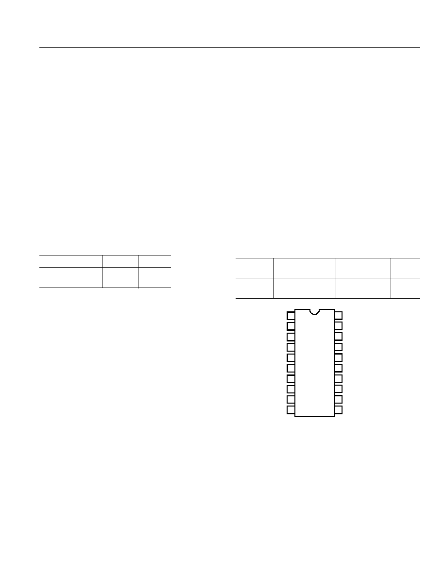
OFFSET 1
OFFSET 2
SIGNAL REFERENCE
SIGNAL OUTPUT
FEEDBACK
OUTPUT FILTER
A1 FILTER
A2 FILTER
EXC 1
EXC 2
LEVEL 1
LEVEL 2
FREQ 1
FREQ 2
B1 FILTER
B2 FILTER
1
2
3
4
5
6
7
8
9
10
11
12
13
14
16
15
17
18
19
20
V
S
+V
S
AD598
TOP VIEW
(Not to Scale)
V
B
V
A
REV. A
3
AD598Typical Characteristics
(at +25 C and V
S
= 15 V, unless otherwise noted)
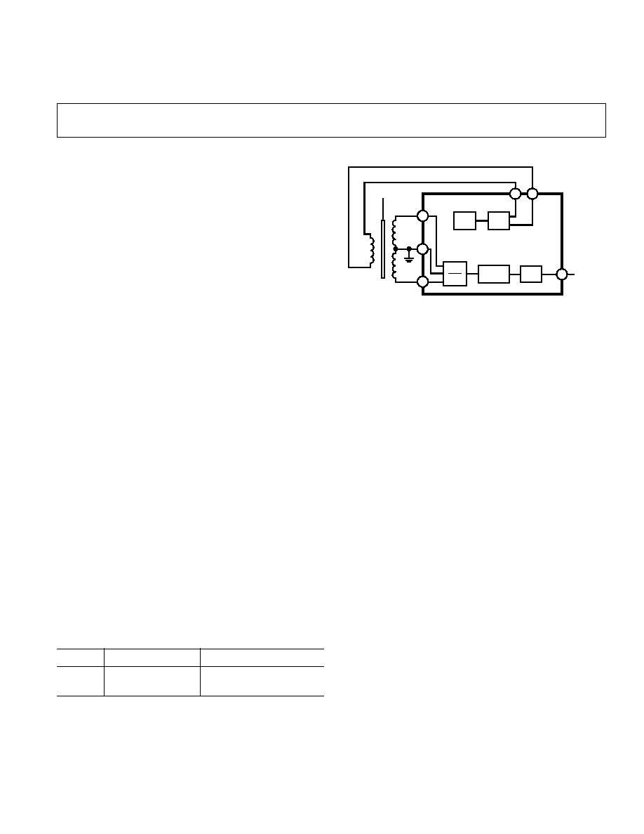
THEORY OF OPERATION
A block diagram of the AD598 along with an LVDT (Linear
Variable Differential Transformer) connected to its input is
shown in Figure 5. The LVDT is an electromechanical trans-
ducer whose input is the mechanical displacement of a core and
whose output is a pair of ac voltages proportional to core posi-
tion. The transducer consists of a primary winding energized by
OSC
AMP
AMP
V
OUT
LVDT
EXCITATION (CARRIER)
11
17
10
16
2
3
FILTER
AB
A+B
V
B
V
A
AD598
Figure 5. AD598 Functional Block Diagram
an external sine wave reference source, two secondary windings
connected in series, and the moveable core to couple flux be-
tween the primary and secondary windings.
The AD598 energizes the LVDT primary, senses the LVDT
secondary output voltages and produces a dc output voltage
proportional to core position. The AD598 consists of a sine
wave oscillator and power amplifier to drive the primary, a de-
coder which determines the ratio of the difference between the
LVDT secondary voltages divided by their sum, a filter and an
output amplifier.
The oscillator comprises a multivibrator which produces a
triwave output. The triwave drives a sine shaper, which pro-
duces a low distortion sine wave whose frequency is determined
by a single capacitor. Output frequency can range from 20 Hz to
20 kHz and amplitude from 2 V rms to 24 V rms. Total har-
monic distortion is typically 50 dB.
The output from the LVDT secondaries consists of a pair of
sine waves whose amplitude difference, (V
A
V
B
), is proportional
to core position. Previous LVDT conditioners synchronously
detect this amplitude difference and convert its absolute value to
20
0
20
60
100
140
60
200
240
160
120
80
40
0
40
TEMPERATURE
°
C
GAIN AND OFFSET PSRR ppm/Volt
OFFSET PSRR 1215V
OFFSET PSRR 1518V
GAIN PSRR 1215V
GAIN PSRR 1518V
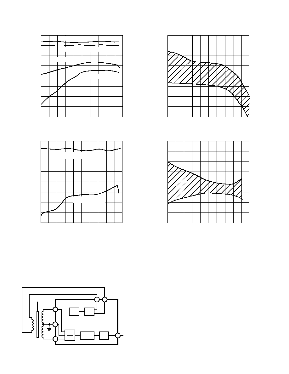
Figure 1. Gain and Offset PSRR vs. Temperature
20
0
20
60
100
140
60
25
30
35
20
15
10
5
0
5
TEMPERATURE
°
C
GAIN AND OFFSET CMRR ppm/Volt
OFFSET CMRR
±
3V
GAIN CMRR
±
3V
Figure 3. Gain and Offset CMRR vs. Temperature
20
0
20
60
100
140
60
40
60
80
20
0
20
40
80
120
TEMPERATURE
°
C
TYPICAL GAIN DRIFT ppm/
°
C
Figure 2. Typical Gain Drift vs. Temperature
20
0
20
60
100
140
60
10
20
0
10
20
TEMPERATURE
°
C
TYPICAL OFFSET DRIFT ppm/
°
C
Figure 4. Typical Offset Drift vs. Temperature
REV. A
4
AD598
REV. A
5
a voltage proportional to position. This technique uses the pri-
mary excitation voltage as a phase reference to determine the
polarity of the output voltage. There are a number of problems
associated with this technique such as (1) producing a constant
amplitude, constant frequency excitation signal, (2) compensating
for LVDT primary to secondary phase shifts, and (3) compen-
sating for these shifts as a function of temperature and frequency.
The AD598 eliminates all of these problems. The AD598 does
not require a constant amplitude because it works on the ratio of
the difference and sum of the LVDT output signals. A constant
frequency signal is not necessary because the inputs are rectified
and only the sine wave carrier magnitude is processed. There is
no sensitivity to phase shift between the primary excitation and
the LVDT outputs because synchronous detection is not em-
ployed. The ratiometric principle upon which the AD598 oper-
ates requires that the sum of the LVDT secondary voltages
remains constant with LVDT stroke length. Although LVDT
manufacturers generally do not specify the relationship between
V
A
+V
B
and stroke length, it is recognized that some LVDTs do
not meet this requirement. In these cases a nonlinearity will
result. However, the majority of available LVDTs do in fact
meet these requirements.
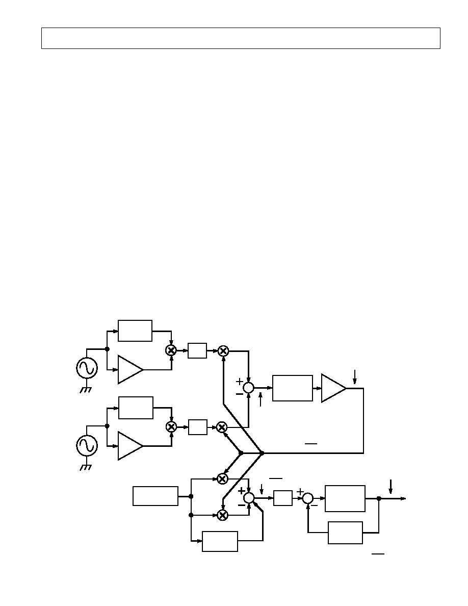
The AD598 utilizes a special decoder circuit. Referring to the
block diagram and Figure 6 below, an implicit analog comput-
ing loop is employed. After rectification, the A and B signals are
multiplied by complementary duty cycle signals, d and (Id)
respectively. The difference of these processed signals is inte-
grated and sampled by a comparator. It is the output of this
comparator that defines the original duty cycle, d, which is fed
back to the multipliers.
As shown in Figure 6, the input to the integrator is [(A+B)d]B.
Since the integrator input is forced to 0, the duty cycle d =
B/(A+B).
The output comparator which produces d = B/(A+B) also con-
trols an output amplifier driven by a reference current. Duty
cycle signals d and (1d) perform separate modulations on the
reference current as shown in Figure 6, which are summed. The
summed current, which is the output current, is I
REF
×
(12d).
Since d = B/(A+B), by substitution the output current equals
I
REF
×
(AB)/(A+B). This output current is then filtered and
converted to a voltage since it is forced to flow through the scal-
ing resistor R2 such that:
V
OUT
=
I
REF
×
( A B ) / (A
+
B )
×
R2
CONNECTING THE AD598
The AD598 can easily be connected for dual or single supply
operation as shown in Figures 7 and 12. The following general
design procedures demonstrate how external component values
are selected and can be used for any LVDT which meets AD598
input/output criteria.
Parameters which are set with external passive components in-
clude: excitation frequency and amplitude, AD598 system
bandwidth, and the scale factor (V/inch). Additionally, there are
optional features, offset null adjustment, filtering, and signal in-
tegration which can be used by adding external components.
COMP
COMP
FILT
FILT
COMP
RTO
OFFSET
FILT
INTEG
V TO I
BANDGAP
REFERENCE
INPUT
INPUT
±
1
±
1
A
d
B
0<d<1
BINARY SIGNAL
d - DUTY CYCLE
(A+B) dB
q
B
A+B
1d
I
REF
d
I
REF
q
AB
A+B
VOLTS
OUTPUT
V
OUT
= R
SCALE
x I
REF
x AB
A+B
INTEG
V TO I
1d
d
V TO I
Figure 6. Block Diagram of Decoder