 | ÐлекÑÑоннÑй компоненÑ: AD602S | СкаÑаÑÑ:  PDF PDF  ZIP ZIP |
AD600/AD602* Dual, Low Noise, Wideband Variable Gain Amplifiers
REV. A
Information furnished by Analog Devices is believed to be accurate and
reliable. However, no responsibility is assumed by Analog Devices for its
use, nor for any infringements of patents or other rights of third parties
which may result from its use. No license is granted by implication or
otherwise under any patent or patent rights of Analog Devices.
a
Dual, Low Noise, Wideband
Variable Gain Amplifiers
AD600/AD602*
One Technology Way, P.O. Box 9106, Norwood, MA 02062-9106, U.S.A.
Tel: 617/329-4700
Fax: 617/326-8703
FEATURES
Two Channels with Independent Gain Control
"Linear in dB" Gain Response
Two Gain Ranges:
AD600: 0 dB to +40 dB
AD602: 10 dB to +30 dB
Accurate Absolute Gain: 0.3 dB
Low Input Noise: 1.4 nV/
Hz
Low Distortion: 60 dBc THD at 1 V Output
High Bandwidth: DC to 35 MHz (3 dB)
Stable Group Delay: 2 ns
Low Power: 125 mW (max) per Amplifier
Signal Gating Function for Each Amplifier
Drives High Speed A/D Converters
MIL-STD-883 Compliant and DESC Versions Available
APPLICATIONS
Ultrasound and Sonar Time-Gain Control
High Performance Audio and RF AGC Systems
Signal Measurement
PRODUCT DESCRIPTION
The AD600 and AD602 dual channel, low noise variable gain
amplifiers are optimized for use in ultrasound imaging systems,
but are applicable to any application requiring very precise gain,
low noise and distortion, and wide bandwidth. Each indepen-
dent channel provides a gain of 0 dB to +40 dB in the AD600
and 10 dB to +30 dB in the AD602. The lower gain of the
AD602 results in an improved signal-to-noise ratio at the out-
put. However, both products have the same 1.4 nV/
Hz
input
noise spectral density. The decibel gain is directly proportional
to the control voltage, is accurately calibrated, and is supply-
and temperature-stable.
To achieve the difficult performance objectives, a proprietary
circuit form--the X-AMP®--has been developed. Each channel
of the X-AMP comprises a variable attenuator of 0 dB to
42.14 dB followed by a high speed fixed gain amplifier. In this
way, the amplifier never has to cope with large inputs, and can
benefit from the use of negative feedback to precisely define the
gain and dynamics. The attenuator is realized as a seven-stage
R-2R ladder network having an input resistance of 100
, laser-
trimmed to
±
2%. The attenuation between tap points is 6.02 dB;
the gain-control circuit provides continuous interpolation be-
tween these taps. The resulting control function is linear in dB.
X-AMP is a registered trademark of Analog Devices, Inc.
*Patented.
The gain-control interfaces are fully differential, providing an
input resistance of ~15 M
and a scale factor of 32 dB/V (that
is, 31.25 mV/dB) defined by an internal voltage reference. The
response time of this interface is less than 1
µ
s. Each channel
also has an independent gating facility that optionally blocks sig-
nal transmission and sets the dc output level to within a few mil-
livolts of the output ground. The gating control input is TTL
and CMOS compatible.
The maximum gain of the AD600 is 41.07 dB, and that of the
AD602 is 31.07 dB; the 3 dB bandwidth of both models is
nominally 35 MHz, essentially independent of the gain. The
signal-to-noise ratio (SNR) for a 1 V rms output and a 1 MHz
noise bandwidth is typically 76 dB for the AD600 and 86 dB for
the AD602. The amplitude response is flat within
±
0.5 dB from
100 kHz to 10 MHz; over this frequency range the group delay
varies by less than
±
2 ns at all gain settings.
Each amplifier channel can drive 100
load impedances with
low distortion. For example, the peak specified output is
±
2.5 V
minimum into a 500
load, or
±
1 V into a 100
load. For a
200
load in shunt with 5 pF, the total harmonic distortion for
a
±
1 V sinusoidal output at 10 MHz is typically 60 dBc.
The AD600J and AD602J are specified for operation from 0
°
C
to +70
°
C, and are available in both 16-pin plastic DIP (N) and
16-pin SOIC (R). The AD600A and AD602A are specified for
operation from 40
°
C to +85
°
C and are available in both 16-pin
cerdip (Q) and 16-pin SOIC (R).
The AD600S and AD602S are specified for operation from
55
°
C to +125
°
C and are available in a 16-pin cerdip (Q) pack-
age and are MIL-STD-883 compliant. The AD600S and
AD602S are also available under DESC SMD 5962-94572.
FUNCTIONAL BLOCK DIAGRAM
GAIN CONTROL
INTERFACE
V
G
RF1
20
PRECISION PASSIVE
INPUT ATTENUATOR
FIXED GAIN
AMPLIFIER
RF2
2.24k
(AD600)
694
(AD602)
A1OP
A1CM
C1HI
C1LO
SCALING
REFERENCE
GATING
INTERFACE
GAT1
41.07dB (AD600)
31.07dB (AD602)
500
62.5
0dB
6.02dB 12.04dB 18.06dB
22.08dB 30.1dB 36.12dB 42.14dB
R 2R LADDER NETWORK
A1HI
A1LO

AD600J/AD602J
AD600A/AD602A
Parameter
Conditions
Min
Typ
Max
Min
Typ
Max
Units
INPUT CHARACTERISTICS
Input Resistance
Pins 2 to 3; Pins 6 to 7
98
100
102
95
100
105
Input Capacitance
2
2
pF
Input Noise Spectral Density
1
1.4
1.4
nV/
Hz
Noise Figure
R
S
= 50
, Maximum Gain
5.3
5.3
dB
R
S
= 200
, Maximum Gain
2
2
dB
Common-Mode Rejection Ratio
f = 100 kHz
30
30
dB
OUTPUT CHARACTERISTICS
3 dB Bandwidth
V
OUT
= 100 mV rms
35
35
MHz
Slew Rate
275
275
V/
µ
s
Peak Output
2
R
L
500
±
2.5
±
3
±
2.5
±
3
V
Output Impedance
f
10 MHz
2
2
Output Short-Circuit Current
50
50
mA
Group Delay Change vs. Gain
f = 3 MHz; Full Gain Range
±
2
±
2
ns
Group Delay Change vs. Frequency
V
G
= 0 V, f = 1 MHz to 10 MHz
±
2
±
2
ns
Total Harmonic Distortion
R
L
= 200
, V
OUT
=
±
1 V Peak, Rpd = 1 k
60
60
dBc
ACCURACY
AD600
Gain Error
0 dB to 3 dB Gain
0
+0.5
+1
0.5
+0.5
+0.5
dB
3 dB to 37 dB Gain
0.5
±
0.2
+0.5
0.1
±
0.2
+1.0
dB
37 dB to 40 dB Gain
1
0.5
0
1.5
0.5
+0.5
dB
Maximum Output Offset Voltage
3
V
G
= 625 mV to +625 mV
10
50
10
65
mV
Output Offset Variation
V
G
= 625 mV to +625 mV
10
50
10
65
mV
AD602
Gain Error
10 dB to 7 dB Gain
0
+0.5
+1
0.5
+0.5
+1.5
dB
7 dB to 27 dB Gain
0.5
±
0.2
+0.5
0.1
±
0.2
+1.0
dB
27 dB to 30 dB Gain
1
0.5
0
1.5
0.5
+0.5
dB
Maximum Output Offset Voltage
3
V
G
= 625 mV to +625 mV
5
30
10
45
mV
Output Offset Variation
V
G
= 625 mV to +625 mV
5
30
10
45
mV
GAIN CONTROL INTERFACE
Gain Scaling Factor
3 dB to 37 dB (AD600); 7 dB to 27 dB (AD602)
31.7
32
32.3
30.5
32
33.5
dB/V
Common-Mode Range
0.75
2.5
0.75
2.5
V
Input Bias Current
0.35
1
0.35
1
µ
A
Input Offset Current
10
50
10
50
nA
Differential Input Resistance
Pins I to 16; Pins 8 to 9
15
15
50
M
Response Rate
Full 40 dB Gain Change
40
40
dB/
µ
s
SIGNAL GATING INTERFACE
Logic Input "LO" (Output ON)
0.8
0.8
V
Logic Input "HI" (Output OFF)
2.4
2.4
V
Response Time
ON to OFF, OFF to ON
0.3
0.3
µ
s
Input Resistance
Pins 4 to 3 Pins 5 to 6
30
30
k
Output Gated OFF
Output Offset Voltage
±
10
100
±
10
400
mV
Output Noise Spectral Density
65
65
nV/
Hz
Signal Feedthrough @ 1 MHz
AD600
80
80
dB
AD602
70
70
dB
POWER SUPPLY
Specified Operating Range
±
4.75
±
5.25
±
4.75
±
5.25
V
Quiescent Current
11
12.5
11
14
mA
NOTES
1
Typical open or short-circuited input; noise is lower when system is set to maximum gain and input is short-circuited. This figure includes the effects of both voltage
and current noise sources.
2
Using resistive loads of 500
or greater, or with the addition of a 1 k
pull-down resistor when driving lower loads
3
The dc gain of the main amplifier in the AD600 is X113; thus an input offset of only 100
µ
V becomes an 11.3 mV output offset. In the AD602, the amplifier's gain is
X35.7; thus, an input offset of 100
µ
V becomes a 3.57 mV output offset.
Specifications shown in boldface are tested on all production units at final electrical test Results from those tests are used to calculate outgoing quality levels. All min
and max specifications guaranteed, although only those shown in boldface are tested on all production units.
Specifications subject to change without notice.
AD600/AD602SPECIFICATIONS
(Each amplifier section, at T
A
= +25 C, V
S
= 5 V, 625 mV
V
G
+625 mV, R
L
= 500 , and C
L
= 5 pF, unless otherwise noted. Specifications for AD600 and AD602 are identical unless otherwise noted.)
2
REV. A
AD600/AD602
REV. A
3
ABSOLUTE MAXIMUM RATINGS
1
Supply Voltage
±
V
S . . . . . . . . . . . . . . . . . . . . . . . . . . . . . . . . . . . . . . . . .
±
7.5 V
Input Voltages
Pins 1, 8, 9, 16 . . . . . . . . . . . . . . . . . . . . . . . . . . . . . . . .
±
V
S
Pins 2, 3, 6, 7 . . . . . . . . . . . . . . . . . . . . . . .
±
2 V Continuous
. . . . . . . . . . . . . . . . . . . . . . . . .
±
V
S
for 10 ms
Pins 4, 5 . . . . . . . . . . . . . . . . . . . . . . . . . . . . . . . . . . . . .
±
V
S
Internal Power Dissipation
2
. . . . . . . . . . . . . . . . . . . . 600 mW
Operating Temperature Range (J) . . . . . . . . . . . 0
°
C to +70
°
C
Operating Temperature Range (A) . . . . . . . . . 40
°
C to +85
°
C
Operating Temperature Range (S) . . . . . . . . . 55
°
C to +125
°
C
Storage Temperature Range . . . . . . . . . . . . . 65
°
C to +150
°
C
Lead Temperature Range (Soldering 60 sec) . . . . . . . . +300
°
C
NOTES
1
Stresses above those listed under "Absolute Maximum Ratings" may cause
permanent damage to the device. This is a stress rating only and functional
operation of the device at these or any other conditions above those indicated in the
operational section of this specification is not implied. Exposure to absolute
maximum rating conditions for extended periods may affect device reliability.
2
Thermal Characteristics: 16-Pin Plastic Package:
JA
= 85
°
C/Watt
16-Pin SOIC Package:
JA
= 100
°
C/Watt
16-Pin Cerdip Package:
JA
= 120
°
C/Watt
ORDERING GUIDE
Gain
Temperatue
Package
Model
Range
Range
Option
1
AD600AQ
0 dB to +40 dB
40
°
C to +85
°
C
Q-16
AD600AR
0 dB to +40 dB
40
°
C to +85
°
C
R-16
AD602AQ
10 dB to +30 dB
40
°
C to +85
°
C
Q-16
AD602AR
10 dB to +30 dB
40
°
C to +85
°
C
R-16
AD600JN
0 dB to +40 dB
0
°
C to +70
°
C
N-16
AD600JR
0 dB to +40 dB
0
°
C to +70
°
C
R-16
AD602JN
10 dB to +30 dB
0
°
C to +70
°
C
N-16
AD602JR
10 dB to +30 dB
0
°
C to +70
°
C
R-16
AD600SQ/883B
2
0 dB to +40 dB
55
°
C to +150
°
C Q-16
AD602SQ/883B
3
10 dB to +30 dB
55
°
C to +150
°
C Q-16
NOTES
1
N = Plastic DIP; Q= Cerdip; R= Small Outline IC (SOIC).
2
Refer to AD600/AD602 Military data sheet. Also available as 5962-9457201MPA.
3
Refer to AD600/AD602 Military data sheet. Also available as 5962-9457202MPA.
PIN DESCRIPTION
Pin
Function
Description
Pin 1
C1LO
CH1 Gain-Control Input "LO" (Positive
Voltage Reduces CH1 Gain).
Pin 2
A1HI
CH1 Signal Input "HI" (Positive Voltage
Increases CH1 Output).
Pin 3
A1LO
CH1 Signal Input "LO" (Usually Taken to
CH1 Input Ground)
Pin 4
GAT1
CH1 Gating Input (A Logic "HI" Shuts Off
CH1 Signal Path).
Pin 5
GAT2
CH2 Gating Input (A Logic "HI" Shuts Off
CH2 Signal Path).
Pin 6
A2LO
CH2 Signal Input "LO" (Usually Taken to
CH2 Input Ground).
Pin 7
A2HI
CH2 Signal Input "HI" (Positive Voltage
Increases CH2 Output).
Pin 8
C2LO
CH2 Gain-Control Input "LO" (Positive
Voltage Reduces CH2 Gain).
Pin 9
C2HI
CH2 Gain-Control Input "HI" (Positive
Voltage Increases CH2 Gain).
Pin 10 A2CM
CH2 Common (Usually Taken to CH2
Output Ground).
Pin 11 A2OP
CH2 Output.
Pin 12 VNEG
Negative Supply for Both Amplifiers.
Pin 13 VPOS
Positive Supply for Both Amplifiers.
Pin 14 A1OP
CH1 Output.
Pin 15 A1CM
CH1 Common (Usually Taken to CH1
Output Ground).
Pin 16 C1HI
CH1 Gain-Control Input "HI" (Positive
Voltage Increases CH1 Gain).
CONNECTION DIAGRAM
16-Pin Plastic DIP (N) Package
16-Pin Plastic SOIC (R) Package
16-Pin Cerdip (Q) Package
1
2
3
4
5
6
7
8
16
15
14
13
12
11
10
9
REF
A1
A2
C1HI
A1CM
A1OP
VPOS
VNEG
A2OP
A2CM
C2HI
C1LO
A1HI
A1LO
GAT1
GAT2
A2LO
A2HI
C2LO
AD600/AD602
CAUTION
ESD (electrostatic discharge) sensitive device. Permanent damage may occur on unconnected
devices subject to high energy electrostatic fields. Unused devices must be stored in conductive
foam or shunts. The protective foam should be discharged to the destination socket before
devices are removed.
WARNING!
ESD SENSITIVE DEVICE
AD600/AD602
REV. A
4
THEORY OF OPERATION
The AD600 and AD602 have the same general design and fea-
tures. They comprise two fixed gain amplifiers, each preceded
by a voltage-controlled attenuator of 0 dB to 42.14 dB with in-
dependent control interfaces, each having a scaling factor of
32 dB per volt. The gain of each amplifier in the AD600 is laser
trimmed to 41.07 dB (X113), thus providing a control range of
1.07 dB to 41.07 dB (0 dB to 40 dB with overlap), while the
AD602 amplifiers have a gain of 31.07 dB (X35.8) and provide
an overall gain of 11.07 dB to 31.07 dB (10 dB to 30 dB with
overlap).
The advantage of this topology is that the amplifier can use
negative feedback to increase the accuracy of its gain; also, since
the amplifier never has to handle large signals at its input, the
distortion can be very low. A further feature of this approach is
that the small-signal gain and phase response, and thus the
pulse response, are essentially independent of gain.
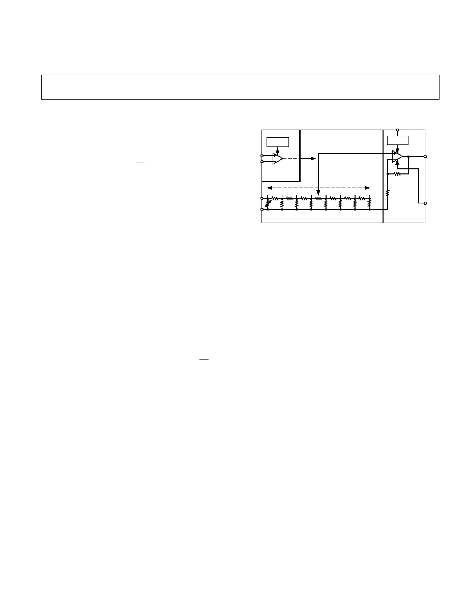
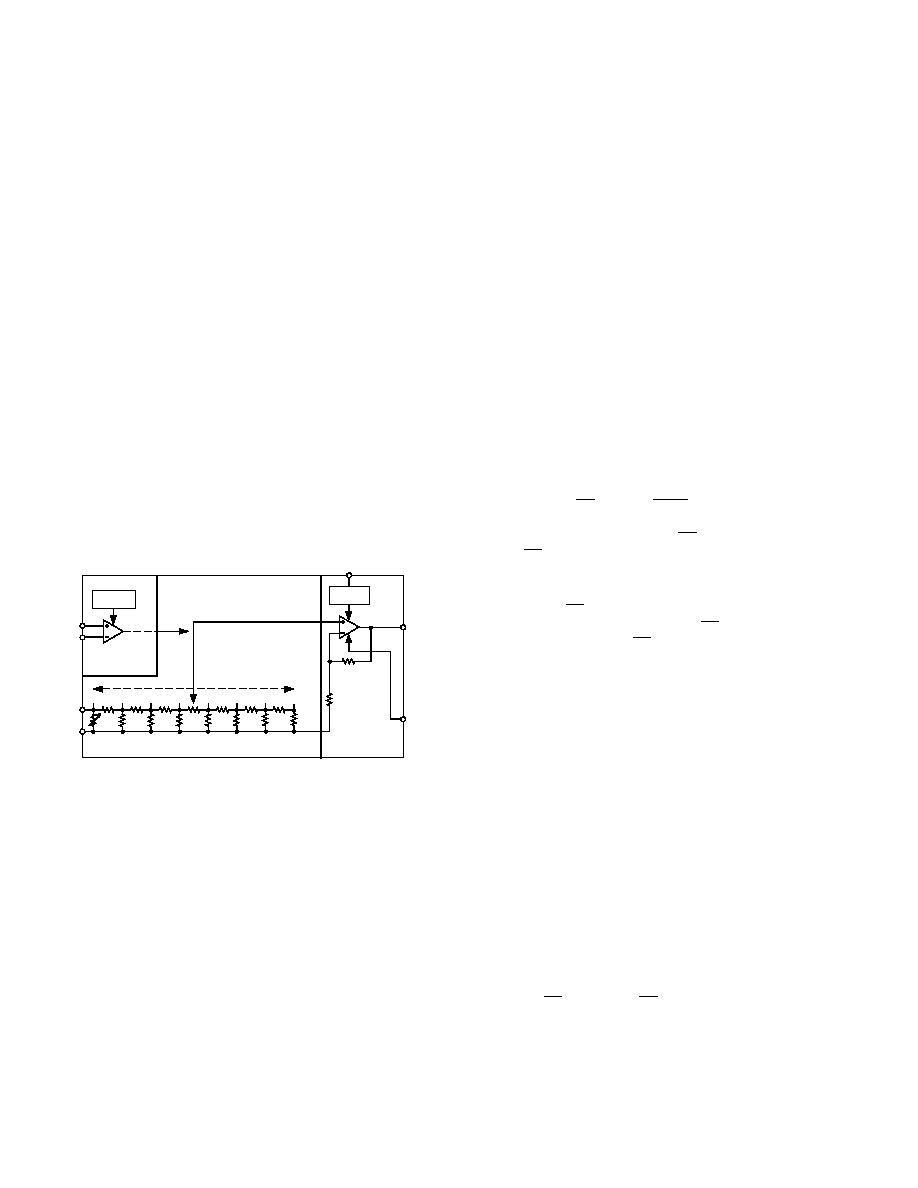
The following discussion describes the AD600. Figure 1 is a
simplified schematic of one channel. The input attenuator is a
seven-section R-2R ladder network, using untrimmed resistors
of nominally R = 62.5
, which results in a characteristic resis-
tance of 125
±
20%. A shunt resistor is included at the input
and laser trimmed to establish a more exact input resistance of
100
±
2%, which ensures accurate operation (gain and HP
corner frequency) when used in conjunction with external resis-
tors or capacitors.
GAIN CONTROL
INTERFACE
V
G
RF1
20
PRECISION PASSIVE
INPUT ATTENUATOR
FIXED GAIN
AMPLIFIER
RF2
2.24k
(AD600)
694
(AD602)
A1OP
A1CM
C1HI
C1LO
SCALING
REFERENCE
GATING
INTERFACE
GAT1
41.07dB (AD600)
31.07dB (AD602)
500
62.5
0dB
6.02dB 12.04dB 18.06dB
22.08dB 30.1dB 36.12dB 42.14dB
R 2R LADDER NETWORK
A1HI
A1LO
Figure 1. Simplified Block Diagram of Single Channel of
the AD600 and AD602
The nominal maximum signal at input A1HI is 1 V rms (
±
1.4 V
peak) when using the recommended
±
5 V supplies, although
operation to
±
2 V peak is permissible with some increase in HF
distortion and feedthrough. Each attenuator is provided with a
separate signal "LO" connection, for use in rejecting common-
mode, the voltage between input and output grounds. Circuitry
is included to provide rejection of up to
±
100 mV.
The signal applied at the input of the ladder network is attenu-
ated by 6.02 dB by each section; thus, the attenuation to each of
the taps is progressively 0, 6.02, 12.04, 18.06, 24.08, 30.1, 36.12
and 42.14 dB. A unique circuit technique is employed to inter-
polate between these tap points, indicated by the "slider" in Fig-
ure 1, providing continuous attenuation from 0 dB to 42.14 dB.
It will help, in understanding the AD600, to think in terms of a
mechanical means for moving this slider from left to right; in
fact, it is voltage controlled. The details of the control interface
are discussed later. Note that the gain is at all times exactly de-
termined, and a linear decibel relationship is automatically guar-
anteed between the gain and the control parameter which
determines the position of the slider. In practice, the gain devi-
ates from the ideal law, by about
±
0.2 dB peak (see, for ex-
ample, Figure 6).
Note that the signal inputs are not fully differential: A1LO and
A1CM (for CH1) and A2LO and A2CM (for CH2) provide
separate access to the input and output grounds. This recog-
nizes the practical fact that even when using a ground plane,
small differences will arise in the voltages at these nodes. It is
important that A1LO and A2LO be connected directly to the
input ground(s); significant impedance in these connections will
reduce the gain accuracy. A1CM and A2CM should be con-
nected to the load ground(s).
Noise Performance
An important reason for using this approach is the superior
noise performance that can be achieved. The nominal resistance
seen at the inner tap points of the attenuator is 41.7
(one
third of 125
), which exhibits a Johnson noise spectral density
(NSD) of 0.84 nV/
Hz
(that is,
4kTR
) at 27
°
C, which is a
large fraction of the total input noise. The first stage of the am-
plifier contributes a further 1.12 nV/
Hz
, for a total input noise
of 1.4 nV/
Hz
.
The noise at the 0 dB tap depends on whether the input is
short-circuited or open-circuited: when shorted, the minimum
NSD of 1.12 nV/
Hz
is achieved; when open, the resistance of
100
at the first tap generates 1.29 nV/
Hz
, so the noise in-
creases to a total of 1.71 nV/
Hz
. (This last calculation would
be important if the AD600 were preceded, for example, by a
900
resistor to allow operation from inputs up to
±
10 V rms.
However, in most cases the low impedance of the source will
limit the maximum noise resistance.)
It will be apparent from the foregoing that it is essential to use a
low resistance in the design of the ladder network to achieve low
noise. In some applications this may be inconvenient, requiring
the use of an external buffer or preamplifier. However, very few
amplifiers combine the needed low noise with low distortion at
maximum input levels, and the power consumption needed to
achieve this performance is fundamentally required to be quite
high (due to the need to maintain very low resistance values
while also coping with large inputs). On the other hand, there is
little value in providing a buffer with high input impedance,
since the usual reason for this--the minimization of loading of a
high resistance source--is not compatible with low noise.
Apart from the small variations just discussed, the signal-to-
noise (S/ N) ratio at the output is essentially independent of the
attenuator setting, since the maximum undistorted output is 1 V
rms and the NSD at the output of the AD600 is fixed at 113
times 1.4 nV/
Hz
, or 158 nV/
Hz
. Thus, in a 1 MHz band-
width, the output S/N ratio would be 76 dB. The input NSD of
the AD600 and AD602 are the same, but because of the 10 dB
lower gain in the AD602's fixed amplifier, its output S/N ratio is
10 dB better, or 86 dB in a 1 MHz bandwidth.
AD600/AD602
REV. A
5
The Gain-Control Interface
The attenuation is controlled through a differential, high imped-
ance (15 M
) input, with a scaling factor which is laser
trimmed to 32 dB per volt, that is, 31.25 mV/dB. Each of the
two amplifiers has its own control interface. An internal band-
gap reference ensures stability of the scaling with respect to
supply and temperature variations, and is the only circuitry
common to both channels.
When the differential input voltage V
G
= 0 V, the attenuator
"slider" is centered, providing an attenuation of 21.07 dB, thus
resulting in an overall gain of 20 dB (= 21.07 dB + 41.07 dB).
When the control input is 625 mV, the gain is lowered by
20 dB (= 0.625
×
32), to 0 dB; when set to +625 mV, the gain
is increased by 20 dB, to 40 dB. When this interface is over-
driven in either direction, the gain approaches either 1.07 dB
(= 42.14 dB + 41.07 dB) or 41.07 dB (= 0 + 41.07 dB),
respectively.
The gain of the AD600 can thus be calculated using the follow-
ing simple expression:
Gain (dB) = 32 V
G
+ 20
(1)
where V
G
is in volts. For the AD602, the expression is:
Gain (dB) = 32 V
G
+ 10
(2)
Operation is specified for V
G
in the range from 625 mV dc to
+625 mV dc. The high impedance gain-control input ensures
minimal loading when driving many amplifiers in multiple-
channel applications. The differential input configuration pro-
vides flexibility in choosing the appropriate signal levels and
polarities for various control schemes.
For example, the gain-control input can be fed differentially to
the inputs, or single-ended by simply grounding the unused in-
put. In another example, if the gain is to be controlled by a
DAC providing a positive only ground referenced output, the
"Gain Control LO" pin (either C1LO or C2LO) should be bi-
ased to a fixed offset of +625 mV, to set the gain to 0 dB when
"Gain Control HI" (C1HI or C2HI) is at zero, and to 40 dB
when at +1.25 V.
It is a simple matter to include a voltage divider to achieve other
scaling factors. When using an 8-bit DAC having a FS output of
+2.55 V (10 mV/bit) a divider ratio of 1.6 (generating 6.25 mV/
bit) would result in a gain setting resolution of 0.2 dB/ bit.
Later, we will discuss how the two sections of an AD600 or
AD602 may be cascaded, when various options exist for gain
control.
Signal-Gating Inputs
Each amplifier section of the AD600 and AD602 is equipped
with a signal gating function, controlled by a TTL or CMOS
logic input (GAT1 or GAT2). The ground references for these
inputs are the signal input grounds A1LO and A2LO, respec-
tively. Operation of the channel is unaffected when this input is
LO or left open-circuited. Signal transmission is blocked when
this input is HI. The dc output level of the channel is set to
within a few millivolts of the output ground (A1CM or A2CM),
and simultaneously the noise level drops significantly. The
reduction in noise and spurious signal feedthrough is useful in
ultrasound beam-forming applications, where many amplifier
outputs are summed.
Common-Mode Rejection
A special circuit technique is used to provide rejection of volt-
ages appearing between input grounds (A1LO and A2LO) and
output grounds (A1CM and A2CM). This is necessary because
of the "op amp" form of the amplifier, as shown in Figure 1.
The feedback voltage is developed across the resistor RF1
(which, to achieve low noise, has a value of only 20
). The
voltage developed across this resistor is referenced to the input
common, so the output voltage is also referred to that node.
To provide rejection of this common voltage, an auxiliary ampli-
fier (not shown) is included, which senses the voltage difference
between input and output commons and cancels this error
component. Thus, for zero differential signal input between
A1HI and A1LO, the output A1OP simply follows the voltage at
A1CM. Note that the range of voltage differences which can ex-
ist between A1LO and A1CM (or A2LO and A2CM) is limited
to about
±
100 mV. Figure 50 (one of the typical performance
curves at the end of this data sheet) shows typical common-
mode rejection ratio versus frequency.
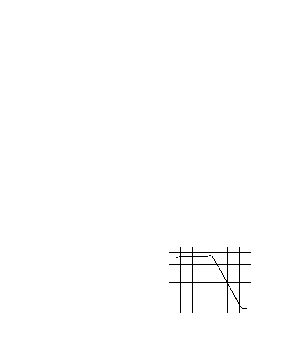
ACHIEVING 80 dB GAIN RANGE
The two amplifier sections of the X-AMP can be connected in
series to achieve higher gain. In this mode, the output of A1
(A1OP and A1CM) drives the input of A2 via a high-pass
network (usually just a capacitor) that rejects the dc offset. The
nominal gain range is now 2 dB to +82 dB for the AD600 or
22 dB to +62 dB for the AD602.
There are several options in connecting the gain-control inputs.
The choice depends on the desired signal-to-noise ratio (SNR)
and gain error (output ripple). The following examples feature
the AD600; the arguments generally apply to the AD602, with
appropriate changes to the gain values.
Sequential Mode (Maximum S/N Ratio)
In the sequential mode of operation, the SNR is maintained at
its highest level for as much of the gain control range possible,
as shown in Figure 2. Note here that the gain range is 0 dB to
80 dB. Figure 3 shows the general connections to accomplish
this. Both gain-control inputs, C1HI and C2HI, are driven in
parallel by a positive only, ground referenced source with a
range of 0 V to +2.5 V.
V
G
S/N RATIO dB
85
30
3.0
45
35
0.0
40
0.5
60
50
55
65
70
75
80
2.5
2.0
1.5
1.0
0.5
Figure 2. S/N Ratio vs. Control Voltage Sequential Control
(1 MHz Bandwidth)