 | ÐлекÑÑоннÑй компоненÑ: AD604-EB | СкаÑаÑÑ:  PDF PDF  ZIP ZIP |
AD604 Dual, Ultralow Noise Variable Gain Amplifier
REV. 0
Information furnished by Analog Devices is believed to be accurate and
reliable. However, no responsibility is assumed by Analog Devices for its
use, nor for any infringements of patents or other rights of third parties
which may result from its use. No license is granted by implication or
otherwise under any patent or patent rights of Analog Devices.
a
Dual, Ultralow Noise
Variable Gain Amplifier
AD604
FEATURES
Ultralow Input Noise at Maximum Gain:
0.80 nV/
Hz, 3.0 pA/
Hz
Two Independent Linear-in-dB Channels
Absolute Gain Range per Channel Programmable:
0 dB to +48 dB (Preamp Gain = +14 dB), through
+6 dB to +54 dB (Preamp Gain = +20 dB)
1.0 dB Gain Accuracy
Bandwidth: 40 MHz (3 dB)
300 k Input Resistance
Variable Gain Scaling: 20 dB/V through 40 dB/V
Stable Gain with Temperature and Supply Variations
Single-Ended Unipolar Gain Control
Power Shutdown at Lower End of Gain Control
Can Drive A/D Converters Directly
APPLICATIONS
Ultrasound and Sonar Time-Gain Control
High Performance AGC Systems
Signal Measurement
PRODUCT DESCRIPTION
The AD604 is an ultralow noise, very accurate, dual channel,
linear-in-dB variable gain amplifier (VGA) optimized for time-
based variable gain control in ultrasound applications; however
it will support any application requiring low noise, wide bandwidth
variable gain control. Each channel of the AD604 provides a
300 k
input resistance and unipolar gain control for ease of
use. User determined gain ranges, gain scaling (dB/V) and dc
level shifting of output further optimize application performance.
Each channel of the AD604 utilizes a high performance pre-
amplifier that provides an input referred noise voltage of
0.8 nV/
Hz
. The very accurate linear-in-dB response of the
AD604 is achieved with the differential input exponential amplifier
(DSX-AMP) architecture. Each of the DSX-AMPs comprise a
variable attenuator of 0 dB to 48.36 dB followed by a high speed
fixed gain amplifier. The attenuator is based on a seven stage
R-1.5R ladder network. The attenuation between tap points
is 6.908 dB and 48.36 dB for the ladder network.
Each independent channel of the AD604 provides a gain range
of 48 dB which can be optimized for the application by program-
ming the preamplifier with a single external resistor in the
preamp feedback path. The linear-in-dB gain response of the
AD604 can be described by the equation: G (dB) = (Gain
Scaling (dB/V )
×
VGN (V )) + (Preamp Gain (dB) 19 dB).
Preamplifier gains between 5 and 10 (+14 dB and +20 dB)
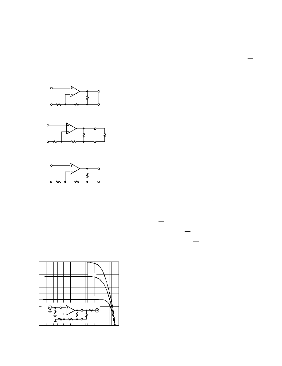
FUNCTIONAL BLOCK DIAGRAM
OUT
VOCM
PAO
PAI
DIFFERENTIAL
ATTENUATOR
+DSX
DSX
VGN
VREF
R-1.5R
LADDER NETWORK
0 TO 48.4dB
PROGRAMMABLE
ULTRALOW NOISE
PREAMPLIFIER
G = 1420dB
PRECISION PASSIVE
INPUT ATTENUATOR
FIXED GAIN
AMPLIFIER
+34.4dB
AFA
GAIN CONTROL
AND SCALING
provide overall gain ranges per channel of 0 dB through +48 dB
and +6 dB through +54 dB. The two channels of the AD604
can be cascaded to provide greater levels of gain range by bypass-
ing the 2nd channel's preamplifier. However, in multiple channel
systems, cascading the AD604 with other devices in the AD60x
VGA family, which do not include a preamplifier may provide
a more efficient solution. The AD604 provides access to the
output of the preamplifier allowing for external filtering be-
tween the preamplifier and the differential attenuator stage.
The gain control interface provides an input resistance of
approximately 2 M
and scale factors from 20 dB/V to
30 dB/V for a V
REF
input voltage of 2.5 V to 1.67 V respect-
ively. Note that scale factors up to 40 dB/V are achievable
with reduced accuracy for scales above 30 dB/V. The gain scales
linear-in-dB with control voltages of 0.4 V to 2.4 V with the
20 dB/V scale. Below and above this gain control range, the gain
begins to deviate from the ideal linear-in-dB control law. The
gain control region below 0.1 V is not used for gain control. In
fact when the gain control voltage is <50 mV the amplifier
channel is powered down to 1.9 mA.
The AD604 is available in a 24-pin plastic SSOP, SOIC and DIP,
and is guaranteed for operation over the 40
°
C to +85
°
C
temperature range.
One Technology Way, P.O. Box 9106, Norwood, MA 02062-9106, U.S.A.
Tel: 617/329-4700
World Wide Web Site: http://www.analog.com
Fax: 617/326-8703
© Analog Devices, Inc., 1996
AD604SPECIFICATIONS
Parameter
Conditions
Min
Typ
Max
Unit
INPUT CHARACTERISTICS
Preamplifier
Input Resistance
300
k
Input Capacitance
8.5
pF
Input Bias Current
27
µ
A
Peak Input Voltage
Preamp Gain = +14 dB
±
400
mV
Preamp Gain = +20 dB
±
200
mV
Input Voltage Noise
VGN
= 2.9 V, R
S
= 0
Preamp Gain = +14 dB
0.8
nV/
Hz
Preamp Gain = +20 dB
0.73
nV/
Hz
Input Current Noise
Independent of Gain
3.0
pA/
Hz
Noise Figure
R
S
= 50
, f = 1 MHz, VGN = 2.9 V
2.3
dB
R
S
= 200
, f =1 MHz, VGN
= 2.9 V
1.1
dB
DSX
Input Resistance
175
Input Capacitance
3.0
pF
Peak Input Voltage
2.5
±
2
V
Input Voltage Noise
VGN
= 2.9 V
1.8
nV/
Hz
Input Current Noise
VGN
= 2.9 V
2.7
pA/
Hz
Noise Figure
R
S
= 50
, f = 1 MHz, VGN = 2.9 V
8.4
dB
R
S
= 200
, f =1 MHz, VGN
= 2.9 V
12
dB
Common-Mode Rejection Ratio
f = 1 MHz, VGN
= 2.65 V
20
dB
OUTPUT CHARACTERISTICS
3 dB Bandwidth
Constant with Gain
40
MHz
Slew Rate
VGN = 1.5 V, Output = 1 V Step
170
V/
µ
s
Output Signal Range
R
L
500
2.5
±
1.5
V
Output Impedance
f = 10 MHz
2
Output Short-Circuit Current
±
40
mA
Harmonic Distortion
VGN
= 1 V, V
OUT
= 1 V p-p
HD2
f = 1 MHz
54
dBc
HD3
f = 1 MHz
67
dBc
HD2
f = 10 MHz
43
dBc
HD3
f = 10 MHz
48
dBc
Two-Tone Intermodulation
VGN = 2.9 V, V
OUT
= 1 V p-p
Distortion (IMD)
f = 1 MHz
74
dBc
f = 10 MHz
71
dBc
3rd Order Intercept
f = 10 MHz, VGN
= 2.65 V,
12.5
dBm
V
OUT
= 1 V p-p, Input Referred
1 dB Compression Point
f = 1 MHz, VGN
= 2.9 V, Output Referred
+15
dBm
Channel-to-Channel Crosstalk
V
OUT
= 1 V p-p, f = 1 MHz
Ch #1: VGN = 2.65 V, Inputs Shorted
30
dB
Ch #2: VGN = 1.5 V (Mid Gain)
dB
Group Delay Variation
1 MHz < f < 10 MHz, Full Gain Range
±
2
ns
V
OCM
Input Resistance
45
k
ACCURACY
Absolute Gain Error
0 dB to +3 dB
0.25 V < VGN < 0.400 V
1.2
+0.75
+3
dB
+3 dB to +43 dB
0.400 V < VGN < 2.400 V
1.0
±
0.3
+1.0
dB
+43 dB to +48 dB
2.400 V < VGN < 2.65 V
3.5
1.25
+1.2
dB
Gain Scaling Error
0.400 V < VGN < 2.400 V
±
0.25
dB/V
Output Offset Voltage
V
REF
= 2.500 V, V
OCM
= 2.500 V
50
±
30
+50
mV
Output Offset Variation
V
REF
= 2.500 V, V
OCM
= 2.500 V
30
50
mV
REV. 0
2
(Each Amplifier Channel at T
A
= +25 C, V
S
= 5 V, R
S
= 50
, R
L
= 500
, C
L
= 5 pF, V
REF
= 2.50 V (Scaling = 20 dB/V), 0 dB to +48 dB gain
range (preamplifier gain = +14 dB), VOCM = 2.5 V, C1 and C2 = 0.1 F (see Figure 35) unless otherwise noted)
REV. 0
3
AD604
Parameter
Conditions
Min
Typ
Max
Unit
GAIN CONTROL INTERFACE
Gain Scaling Factor
V
REF
= 2.5 V, 0.4 V < VGN < 2.4 V
19
20
21
dB/V
V
REF
= 1.67 V
30
dB/V
Gain Range
Preamp Gain = +14 dB
0 to +48
dB
Preamp Gain = +20 dB
+6 to +54
dB
Input Voltage (VGN) Range
20 dB/V, V
REF
= 2.5 V
0.1 to 2.9
V
Input Bias Current
0.4
µ
A
Input Resistance
2
M
Response Time
48 dB Gain Change
0.2
µ
s
V
REF
Input Resistance
10
k
POWER SUPPLY
Specified Operating Range
One Complete Channel
±
5
V
One DSX Only
+5
V
Power Dissipation
One Complete Channel
220
mW
One DSX Only
95
mW
Quiescent Supply Current
VPOS, One Complete Channel
32
36
mA
VPOS, One DSX Only
19
23
mA
VNEG, One Preamplifier Only
15
12
mA
Powered Down
VPOS, VGN < 50 mV, One Channel
1.9
3.0
mA
VNEG, VGN < 50 mV, One Channel
150
µ
A
Power-Up Response Time
48 dB Gain Change, V
OUT
= 2 V p-p
0.6
µ
s
Power-Down Response Time
0.4
µ
s
ABSOLUTE MAXIMUM RATINGS
Supply Voltage
±
V
S
Pins 17, 18, 19, 20 (with Pins 16, 22 = 0 V) . . . . . .
±
6.5 V
Input Voltages
Pins 1, 2, 11, 12 . . . . . . . . . . . . . VPOS/2
±
2 V Continuous
Pins 4, 9 . . . . . . . . . . . . . . . . . . . . . . . . . . . . . . . . . . .
±
2 V
Pins 5, 8 . . . . . . . . . . . . . . . . . . . . . . . . . . . . VPOS, VNEG
Pins 6, 7, 13, 14, 23, 24 . . . . . . . . . . . . . . . . . . . . VPOS, 0
Internal Power Dissipation
Plastic (N) . . . . . . . . . . . . . . . . . . . . . . . . . . . . . . . . . 2.2 W
Small Outline (R) . . . . . . . . . . . . . . . . . . . . . . . . . . . . 1.7 W
Shrink Small Outline (RS) . . . . . . . . . . . . . . . . . . . . . 1.1 W
Operating Temperature Range . . . . . . . . . . . 40
°
C to +85
°
C
Storage Temperature Range . . . . . . . . . . . . 65
°
C to +150
°
C
Lead Temperature, Soldering 60 seconds . . . . . . . . . +300
°
C
NOTES
1
Stresses above those listed under "Absolute Maximum Ratings" may cause
permanent damage to the device. This is a stress rating only and functional opera-
tion of the device at these or any other conditions above those indicated in the
operational section of this specification is not implied. Exposure to absolute maxi-
mum rating conditions for extended periods may affect device reliability.
2
Pins 1, 2, 11, 12, 13, 14, 23, 24 are part of a single-supply circuit and the part will
most likely be damaged if any of these pins are accidentally connected to VN.
3
When driven from an external low impedance source.
ORDERING GUIDE
Temperature
Package
Model
Range
JA
Option*
AD604AN
40
°
C to +85
°
C
57
°
C/W
N-24
AD604AR
40
°
C to +85
°
C
70
°
C/W
R-24
AD604ARS
40
°
C to +85
°
C
112
°
C/W
R-24
*N = Plastic DIP, R = Small Outline IC (SOIC), RS = Shrink Small Outline
Package (SSOP).
WARNING!
ESD SENSITIVE DEVICE
CAUTION
ESD (electrostatic discharge) sensitive device. Electrostatic charges as high as 4000 V readily
accumulate on the human body and test equipment and can discharge without detection.
Although the AD604 features proprietary ESD protection circuitry, permanent damage may
occur on devices subjected to high energy electrostatic discharges. Therefore, proper ESD
precautions are recommended to avoid performance degradation or loss of functionality.
AD604
REV. 0
4
PIN DESCRIPTIONS
Pin No.
Mnemonic
Description
Pin 1
DSX1
CH1 Negative Signal Input to DSX1.
Pin 2
+DSX1
CH1 Positive Signal Input to DSX1.
Pin 3
PAO1
CH1 Preamplifier Output.
Pin 4
FBK1
CH1 Preamplifier Feedback Pin.
Pin 5
PAI1
CH1 Preamplifier Positive Input.
Pin 6
COM1
CH1 Signal Ground; when connected to positive supply, Preamplifier1 will shut down.
Pin 7
COM2
CH2 Signal Ground; when connected to positive supply, Preamplifier2 will shut down.
Pin 8
PAI2
CH2 Preamplifier Positive Input.
Pin 9
FBK2
CH2 Preamplifier Feedback Pin.
Pin 10
PAO2
CH2 Preamplifier Output.
Pin 11
+DSX2
CH2 Positive Signal Input to DSX2.
Pin 12
DSX2
CH2 Negative Signal Input to DSX2.
Pin 13
VGN2
CH2 Gain-Control Input and Power-Down Pin. If grounded, device is off,
otherwise positive voltage increases gain.
Pin 14
VOCM
Input to this pin defines common-mode of output at OUT1 and OUT2.
Pin 15
OUT2
CH2 Signal Output.
Pin 16
GND2
Ground.
Pin 17
VPOS
Positive Supply.
Pin 18
VNEG
Negative Supply.
Pin 19
VNEG
Negative Supply.
Pin 20
VPOS
Positive Supply.
Pin 21
GND1
Ground.
Pin 22
OUT1
CH1 Signal Output.
Pin 23
VREF
Input to this pin sets gain-scaling for both channels +2.5 V = 20 dB/V, +1.67 V = 30 dB/V.
Pin 24
VGN1
CH1 Gain-Control Input and Power-Down Pin. If grounded, device is off;
otherwise positive voltage increases gain.
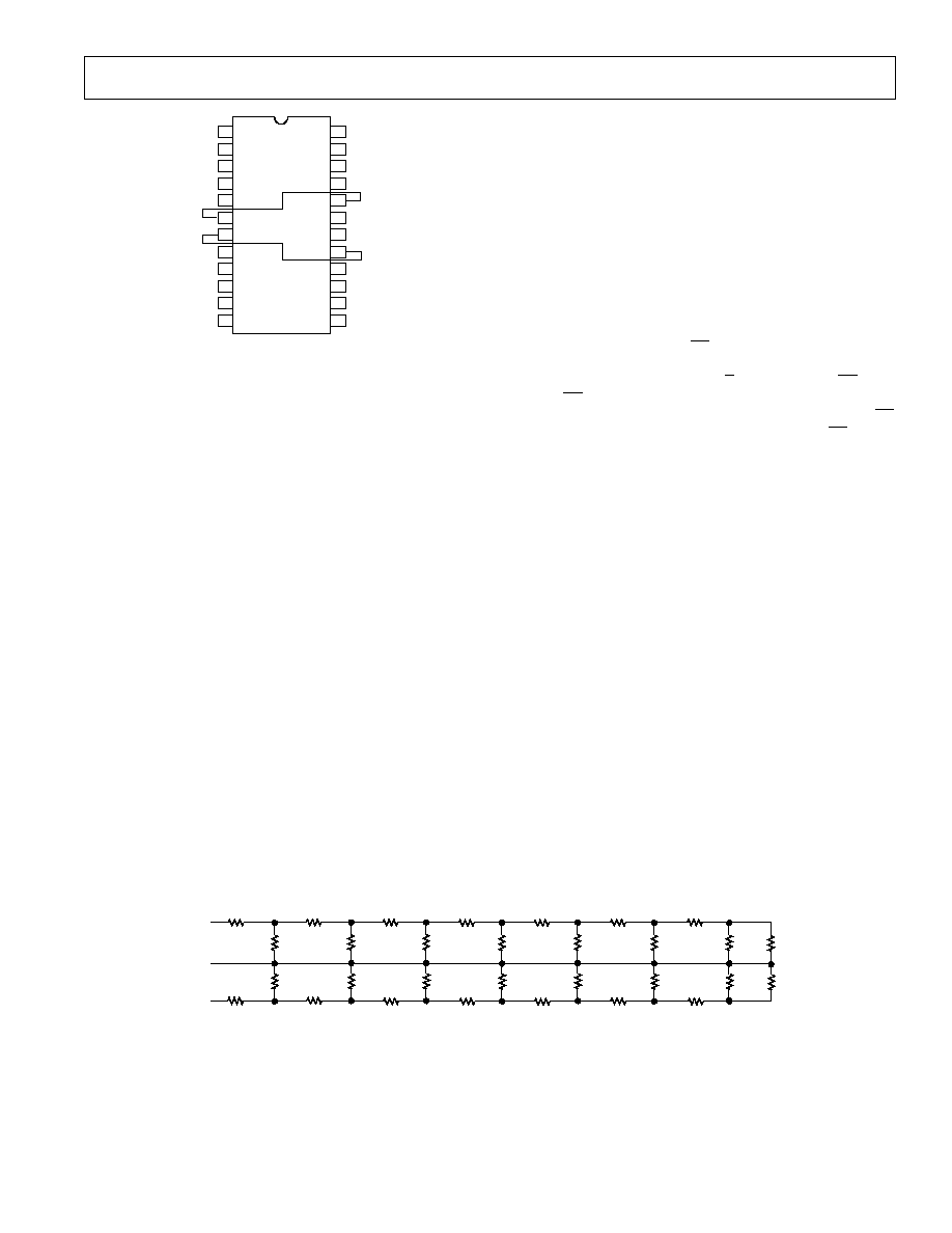
PIN CONFIGURATION
DSX1
+DSX1
PAI1
FBK1
PAO1
COM1
COM2
PAI2
FBK2
PAO2
+DSX2
DSX2
VGN1
VREF
VPOS
GND1
OUT1
VNEG
VNEG
VPOS
GND2
OUT2
VOCM
VGN2
13
16
15
14
24
23
22
21
20
19
18
17
TOP VIEW
(Not to Scale)
12
11
10
9
8
1
2
3
4
7
6
5
AD604
5
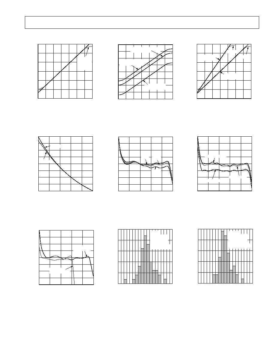
Typical Performance Characteristics (per Channel)AD604
(Unless otherwise noted G (preamp) = +14 dB, V
REF
= 2.5 V (20 dB/V Scaling), f = 1 MHz, R
L
= 500
, C
L
= 5 pF, T
A
= +25 C, V
SS
= 5 V)
VGN Volts
50
20
10
0.1
2.9
40
30
10
0
0.5
0.9
1.3
1.7
2.1
2.5
3 CURVES
40
°
C,
+25
°
C,
+85
°
C
GAIN dB
Figure 1. Gain vs. VGN
GAIN SCALING dB/V
40
37.5
32.5
30
25
20
22.5
27.5
35
1.25
1.5
1.75
2
2.25
2.5
THEORETICAL
ACTUAL
V
REF
Volts
Figure 4. Gain Scaling vs. V
REF
VGN Volts
GAIN ERROR dB
2.0
0.2
1.5
1.0
0.5
0
0.5
1.0
1.5
2.0
0.7
1.2
1.7
2.2
2.7
30dB/V
VREF = 1.67V
20dB/V
VREF = 2.50V
Figure 7. Gain Error vs. VGN for
Different Gain Scalings
VGN Volts
60
0.1
50
40
30
20
10
0
10
20
0.5
0.9
1.3
1.7
2.1
2.5
2.9
G (PREAMP) = +14dB
(0dB +48dB)
G (PREAMP) = +20dB
(+6dB +54dB)
DSX ONLY
(14dB +34dB)
GAIN dB
Figure 2. Gain vs. VGN for Different
Preamp Gains
VGN Volts
GAIN ERROR dB
2.0
0.2
1.5
1.0
0.5
0
0.5
1.0
1.5
2.0
0.7
1.2
1.7
2.2
2.7
+85
°
C
+25
°
C
40
°
C
Figure 5. Gain Error vs. VGN at
Different Temperatures
DELTA GAIN dB
PERCENTAGE
25
1.0
20
15
10
5
0
0.8 0.6 0.4 0.2 0.1 0.3 0.5 0.7 0.9
G(dB) =
G(CH1) G(CH2)
VGN1 = 1.0V
VGN2 = 1.0V
N = 50
Figure 8. Gain Match; VGN1 = VGN2 =
1.0 V
VGN Volts
50
20
10
0.1
2.9
40
30
10
0
0.5
0.9
1.3
1.7
2.1
2.5
ACTUAL
ACTUAL
30dB/V
VREF = 1.67V
20dB/V
VREF
= 2.50V
GAIN dB
Figure 3. Gain vs. VGN for Different
Gain Scalings
VGN Volts
GAIN ERROR dB
2.0
0.2
1.5
1.0
0.5
0
0.5
1.0
1.5
2.0
0.7
1.2
1.7
2.2
2.7
FREQ = 5MHz
FREQ = 10MHz
FREQ = 1MHz
Figure 6. Gain Error vs. VGN at
Different Frequencies
DELTA GAIN dB
PERCENTAGE
25
1.0
20
15
10
5
0
0.8 0.6 0.4 0.2 0.1 0.3 0.5 0.7 0.9
G(dB) =
G(CH1) G(CH2)
VGN1 = 2.50V
VGN2 = 2.50V
N = 50
Figure 9. Gain Match: VGN1 = VGN2 =
2.50 V
REV. 0
REV. 0
6
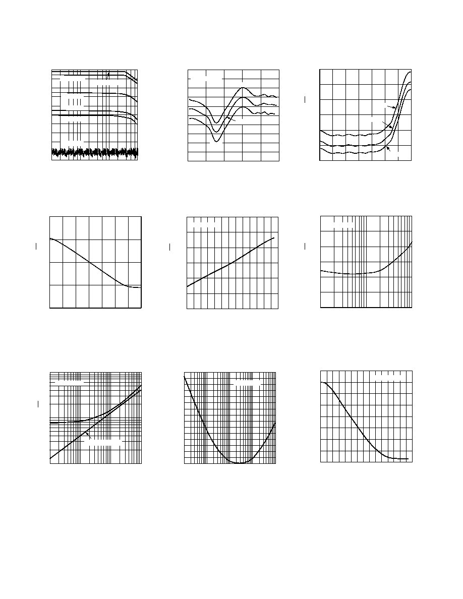
AD604Typical Performance Characteristics (per Channel)
(Unless otherwise noted G (preamp) = +14 dB, V
REF
= 2.5 V (20 dB/V Scaling), f = 1 MHz, R
L
= 500
, C
L
= 5 pF, T
A
= +25 C, V
SS
= 5 V)
FREQUENCY Hz
GAIN dB
50
40
50
100k
1M
10M
100M
30
20
10
0
10
20
30
40
VGN = 1.5V
VGN = 2.9V
VGN = 2.5V
VGN = 0.1V
VGN = 0.5V
VGN = 0.0V
Figure 10. AC Response
NOISE
n
V
/
Hz
VGN Volts
1000
1
0.1
0.1
2.9
100
10
0.5
0.9
1.3
1.7
2.1
2.5
Figure 13. Input Referred Noise vs.
VGN
NOISE
n
V
/
Hz
R
SOURCE
10
1
0.1
1
10
1k
100
R
SOURCE
ALONE
VGN = 2.9V
Figure 16. Input Referred Noise vs.
R
SOURCE
VGN Volts
210
0.1
190
170
150
130
110
90
0.5
0.9
1.3
1.7
2.1
2.5
2.9
+85
°
C
+25
°
C
40
°
C
NOISE
n
V
/
Hz
Figure 12. Output Referred Noise vs.
VGN
NOISE
p
V
/
Hz
FREQUENCY Hz
770
745
740
760
765
750
755
100k
1M
10M
VGN = 2.9V
Figure 15. Input Referred Noise vs.
Frequency
VGN Volts
dB
40
20
0
0
1.2
35
30
25
15
10
5
0.4
0.8
1.6
2.0
2.4
2.8
R
S
= 240
Figure 18. Noise Figure vs. VGN
VGN Volts
2.55
0.2
2.54
2.53
2.52
2.51
2.50
2.49
2.48
2.45
0.7
1.2
1.7
2.2
2.7
40
°
C
+25
°
C
+85
°
C
VOCM = 2.50V
V
OUT
Volts
2.46
2.47
Figure 11. Output Offset vs. VN
NOISE
p
V
/
Hz
900
850
800
750
700
650
600
0
80
TEMPERATURE
°
C
40
20
20
40
60
90
VGN = 2.9V
Figure 14. Input Referred Noise vs.
Temperature
RIN
dB
16
11
1
1
10
10k
100
1k
6
15
14
13
12
10
9
8
7
5
3
4
2
VGN = 2.9V
Figure 17. Noise Figure vs. R
SOURCE
AD604
REV. 0
7
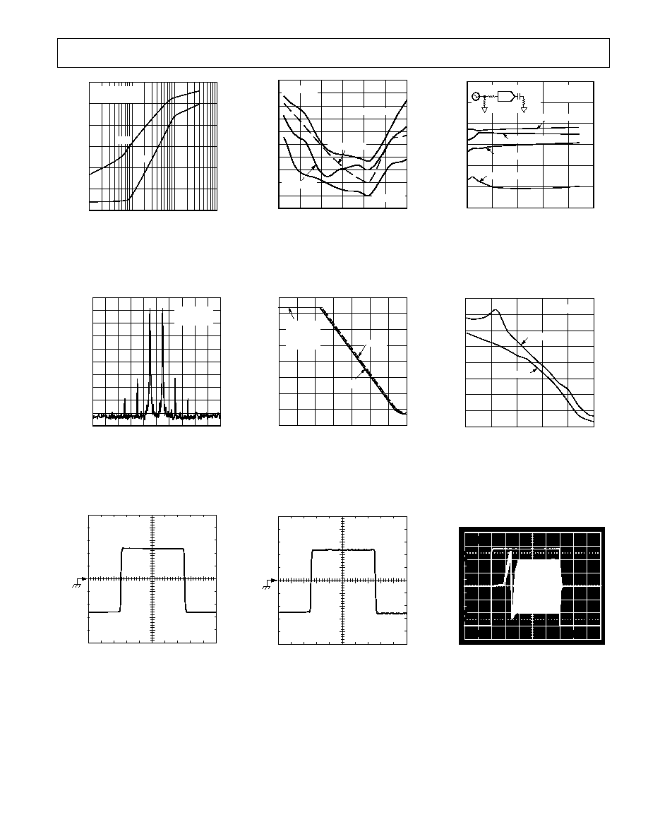
VGN Volts
HARMONIC DISTORTION dBc
30
60
80
0.5
2.1
2.9
40
50
70
0.9
1.3
1.7
2.5
HD2(1MHz)
HD3(1MHz)
V
O
= 1V p-p
HD3(10MHz)
HD2(10MHz)
35
65
45
55
75
Figure 20. Harmonic Distortion vs.
VGN
VGN Volts
P
IN
dBm
5
15
35
0.1
1.3
0
5
10
20
30
25
0.5
0.9
1.7
2.1
10MHz
1MHz
INPUT
SIGNAL
LIMIT
800mV p-p
2.5
2.9
Figure 23. 1 dB Compression vs. VGN
100ns / DIV
40mV / DIV
V
O
= 200mV p-p
VGN = 1.5V
200
200
253ns
1.253µs
TRIG'D
Figure 26. Small Signal Pulse
Response
FREQUENCY Hz
HARMONIC DISTORTION dBc
40
50
70
100k
60
45
55
65
1M
10M
100M
V
O
= 1V p-p
VGN = +1.0V
HD2
HD3
Figure 19. Harmonic Distortion vs.
Frequency
FREQUENCY MHz
P
OUT
dBm
90
120
9.96
9.98
10
10.02
10.04
30
80
100
110
60
70
40
50
V
O
= 1V p-p
VGN = 1.0V
20
Figure 22. Intermodulation Distortion
100ns / DIV
400mV / DIV
V
O
= 2V p-p
VGN = 1.5V
2V
2V
253ns
1.253µs
Figure 25. Large Signal Pulse
Response
R
SOURCE
20
50
80
0
HARMONIC DISTORTION dBc
200
250
30
40
70
60
50
150
100
HD3(10MHz)
HD2(10MHz)
HD3(1MHz)
HD2(1MHz)
R
S
DUT
50
500
V
O
= 1V p-p
VGN = 1.0V
Figure 21. Harmonic Distortion vs.
R
SOURCE
VGN Volts
IP3 dBm
25
20
15
0.4
0.9
2.9
1.4
1.9
2.4
5
0
5
10
15
10
V
O
= 1V p-p
f = 1MHz
f = 10MHz
Figure 24. 3rd Order Intercept vs.
VGN
10
0%
100
90
500mV
200ns
500mV
2.9V
0V
VGN Volts
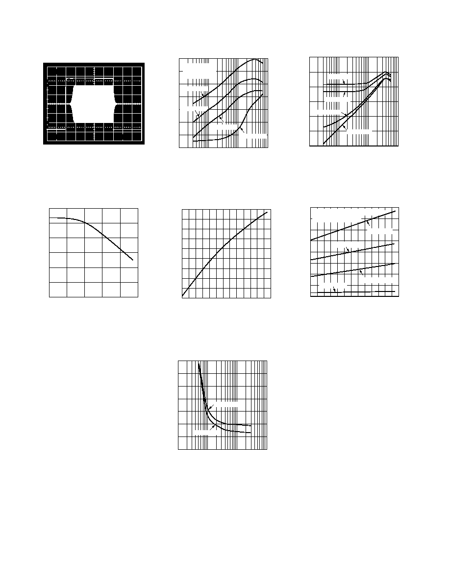
Figure 27. Power-Up/Down Response
AD604
REV. 0
8
FREQUENCY Hz
CROSSTALK dB
30
10
20
40
50
60
0
70
100k
1M
100M
10M
VGN2 = 2.9V
VGN2 = 2.0V
VGN2 = 1.5V
VGN1 = 1V
V
OUT1
= 1V p-p
V
IN2
= GND
VGN2 = 0.1V
Figure 29. Crosstalk (CH1 to CH2) vs.
Frequency
TEMPERATURE
°
C
INPUT BIAS CURRENT µA
27.6
25.8
20
90
27.2
26.8
26.6
26.2
20
0
60
80
40
40
26.0
26.4
27.0
27.4
Figure 32. Input Bias Current vs.
Temperature
FREQUENCY Hz
100k
1M
100M
10M
VGN = 0.1V
VGN = 2.9V
20
14
6
8
10
12
16
18
DELAY ns
Figure 34. Group Delay vs. Frequency
FREQUENCY Hz
CMRR dB
50
10
20
30
40
60
0
100k
1M
100M
10M
VGN = 2.9V
VGN = 0.1V
VGN = 2.0V
VGN = 2.5V
Figure 30. DSX Common-Mode
Rejection vs. Frequency
TEMPERATURE
°
C
SUPPLY CURRENT mA
40
20
0
35
30
25
15
10
5
40
40
90
20
0
20
60
80
AD604 (+I
S
)
DSX (+I
S
)
PRE-AMP (
±
I
S
)
+I
S
(VGN = 0)
I
S
(AD604) = I
S
(PA)
+I
S
(AD604) = +I
S
(PA) + +I
S
(DSX)
Figure 33. Supply Current (One
Channel) vs. Temperature
10
0%
100
90
500mV
100ns
500mV
2.9V
0.1V
VGN Volts
Figure 28. Gain Response
FREQUENCY Hz
1M
1k
1
1k
1M
100M
100k
10k
100
10
10k
100k
INPUT IMPEDANCE
10M
Figure 31. Input Impedance vs.
Frequency
AD604
REV. 0
9
1
To understand the active-feedback amplifier topology, refer to the AD830 data
sheet. The AD830 is a practical implementation of the idea.
THEORY OF OPERATION
The AD604 is a dual channel, variable gain amplifier with an
ultralow noise preamplifier. Figure 35 shows the simplified
block diagram of one channel. Each channel consists of:
(1) a preamplifier with gain setting resistors R5, R6 and R7
(2) a single-supply X-AMP (hereafter called, DSX, Differential
Single-supply X-AMP) made up of:
(a) a precision passive attenuator (differential ladder)
(b) a gain control block
(c) a VOCM buffer with supply splitting resistors R3 and R4
(d) an Active Feedback Amplifier
1
(AFA) with gain setting
resistors R1 and R2
The preamplifier is powered by a
±
5 V supply, while the DSX
uses a single +5 V supply. The linear-in-dB gain response of the
AD604 can generally be described by Equation 1:
G (dB) = (Gain Scaling (dB/V))
×
(Gain Control (V )) +
((Preamp Gain (dB)) 19 dB)
(1)
Each channel provides between 0 dB to +48.4 dB through +6 dB
to +54.4 dB of gain depending on the user determined pream-
plifier gain. The center 40 dB of gain is exactly linear-in-dB
while the gain error increases at the top and bottom of the
range. The gain of the preamplifier is typically either +14 dB or
+20 dB, but can be set to intermediate values by a single exter-
nal resistor (see PREAMPLIFIER section for details). The gain
of the DSX can vary from 14 dB to +34.4 dB which is deter-
mined by the gain control voltage (VGN). The VREF input
establishes the gain scaling the useful gain scaling range is
between 20 dB/V and 40 dB/V for a VREF voltage of 2.5 V and
1.25 V respectively. For example, if the preamp gain was set to
+14 dB and VREF was set to 2.50 V (to establish a gain scaling
of 20 dB/V), the gain equation would simplify to:
G (dB ) = (20 (dB/V ))
×
(VGN (V )) 5 dB
The desired gain can then be achieved by setting the unipolar
gain control (VGN) to a voltage within its nominal operating
range of 0.25 V to 2.65 V (for 20 dB/V gain scaling). The gain is
monotonic for a complete gain control voltage range of 0.1 V to
2.9 V. Maximum gain can be achieved at a VGN of 2.9 V.
Since the two channels are identical, only Channel 1 will be
used to describe their operation. VREF and VOCM are the only
inputs that are shared by the two channels, and since they are
normally ac grounds, crosstalk between the two channels is
minimized. For highest gain scaling accuracy, VREF should
have an external low impedance voltage source. For low accu-
racy 20 dB/V applications, the VREF input can be decoupled
with a capacitor to ground. In this mode the gain scaling will be
determined by the midpoint between +V
CC
and GND, so care
should be taken to control the supply voltage to +5 V. The in-
put resistance looking into the VREF pin is 10 k
±
20%.
The DSX portion of the AD604 is a single-supply circuit and
the VOCM pin is used to establish the dc level of the midpoint
of this portion of the circuit. VOCM needs only an external
decoupling capacitor to ground to center the midpoint between
the supply voltages (+5 V, GND); however, if the dc level of the
output is important to the user (see APPLICATIONS section
for AD9050 example), then VOCM can be specifically set. The
input resistance looking into the VOCM pin is 45 k
±
20%.
Preamplifier
The input capability of the following single-supply DSX (2.5
±
2 V for a +5 V supply) limits the maximum input voltage of the
preamplifier to
±
400 mV for the 14 dB gain configuration or
±
200 mV for the 20 dB gain configuration.
The preamplifier's gain can be programmed to +14 dB or
+20 dB; by either shorting the FBK1 node to PAO1 (+14 dB),
or leaving node FBK1 open (+20 dB). These two gain settings
are very accurate since they are set by the ratio of on-chip resis-
tors. Any intermediate gain can be achieved by connecting the
appropriate resistor value between PAO1 and FBK1 according
to Equations 2 and 3:
G
=
V
OUT
V
IN
=
( R7 R
EXT
)
+
R5
+
R6
R6
(2)
R
EXT
=
[R6
×
G
-
( R5
+
R6)]
×
R7
R7
-
( R6
×
G )
+
( R5
+
R6)
(3)
FBK
C1
R1
820
VREF
VGN
PAI
PAO
+DSX
DSX
EXT.
COM
R5
32
R7
40
R6
8
VPOS
VOCM
R3
200k
C3
C2
OUT
DIFFERENTIAL
ATTENUATOR
DISTRIBUTED G
M
175
175
G1
GAIN
CONTROL
Ao
G2
R2
20
R4
200k
EXT.
Figure 35. Simplified Block Diagram of a Single Channel of the AD604
AD604
REV. 0
10
Since the internal resistors have an absolute tolerance of
±
20%,
the gain can be in error by as much as 0.33 dB when R
EXT
is
30
, where it was assumed that R
EXT
is exact.
Figure 36 shows how the preamplifier is set to gains of +14,
+17.5 and +20 dB. The gain range of a single channel of the
AD604 is 0 dB to +48 dB when the preamplifier is set to
+14 dB (Figure 36a), 3.5 dB to +51.5 dB for a preamp gain of
+17.5 dB (Figure 36b), and 6 dB to 54 dB for the highest
preamp gain of +20 dB (Figure 36c).
FBK1
PAO1
COM1
R5
32
R7
40
R6
8
PAI1
a. Preamp Gain = 14 dB
R10
40
FBK1
PAO1
COM1
R5
32
R7
40
R6
8
PAI1
b. Preamp Gain = 17.5 dB
FBK1
PAO1
COM1
R5
32
R7
40
R6
8
PAI1
c. Preamp Gain = 20 dB
Figure 36. Preamplifier Gain Programmability
For a preamplifier gain of +14 dB, the preamplifier's 3 dB
small-signal bandwidth is 130 MHz; when the gain is at the high
end (+20 dB), the bandwidth will be reduced by a factor of two
to 65 MHz. Figure 37 shows the ac responses for the three preamp
gains discussed above; note that the gain for an R
EXT
of 40
should be 17.5 dB, but the mismatch between the internal resis-
tors and the external resistor has caused the actual gain for this
particular preamplifier to be 17.7 dB. The 3 dB small-signal
bandwidth of one complete channel of the AD604 (preamplifier
and DSX) is 40 MHz and is independent of gain.
R
EXT
20
19
10
100k
1M
GAIN
dB
10M
100M
18
17
16
15
14
13
12
11
OPEN
40
SHORT
50
40
R
EXT
150
8
32
IN
V
IN
Figure 37. AC Responses for Preamplifier Gains Shown in
Figure 36.
To achieve its optimum specifications, power and ground man-
agement are critical to the AD604. Large dynamic currents
result because of the low resistances needed for the desired
noise performance. Most of the difficulty is with the very low
gain setting resistors of the preamplifier that allow for a total
input referred noise, including the DSX, as low as 0.8 nV/
Hz
.
The consequently large dynamic currents have to be carefully
handled to maintain performance even at large signal levels.
To accommodate these large dynamic currents as well as a
ground referenced input, the preamplifier is operated from a
dual
±
5 V supply. This causes the preamplifiers output to also
be ground referenced, which requires a common-mode level
shift into the single-supply DSX. The two external coupling ca-
pacitors (C1, C2 in Figure 35) connected to nodes PAO1 and
+DSX, and DSX and ground, respectively, perform this func-
tion (see AC Coupling Section). In addition, they eliminate any
offset that would otherwise be introduced by the preamplifier. It
should be noted that an offset of 1 mV at the input of the DSX
will get amplified by +34.4 dB (
×
52.5) when the gain-control
voltage is at its maximum, this equates to 52.5 mV at the out-
put. AC coupling is consequently required to keep the offset
from degrading the output signal range.
The internal feedback resistors setting the gain of the preampli-
fier are so small (nominally 8
and 32
) that even an addi-
tional 1
in the "ground" connection at pin COM1, which
serves as the input common-mode reference, will seriously
degrade gain accuracy and noise performance. This node is very
sensitive and careful attention is necessary to minimize the
ground impedance. All connections to node COM1 should be
as short as possible.
The preamplifier including the gain setting resistors has a noise
performance of 0.71 nV/
Hz
and 3 pA/
Hz
. Note that a signifi-
cant portion of the total input referred voltage noise is due to
the feedback resistors. The equivalent noise resistance presented
by R5 and R6 in parallel is nominally 6.4
, which contributes
0.33 nV/
Hz
to the total input referred voltage noise. The larger
portion of the input referred voltage noise is coming from the
amplifier with 0.63 nV/
Hz
. The current noise is independent of
gain and depends only on the bias current in the input stage of
the preamplifier--it is 3 pA/
Hz
.
The preamplifier can drive 40
(the nominal feedback resis-
tors) and the following 175
ladder load of the DSX with low
distortion. For example, at 10 MHz and
±
1 V at the output, the
preamplifier has less than 45 dB of second and third harmonic
distortion when driven from a low (25
) source resistance.
In some cases one may need more than 48 dB of gain range, in
which case two AD604 channels could be cascaded. Since the
preamplifier has limited input signal range, consumes over half
(120 mW) of the total power (220 mW), and its ultralow noise
is not necessary after the first AD604 channel, a shutdown
mechanism that disables only the preamplifier is built in. All
that is required to shut down the preamplifier is to tie the
COM1 and/or COM2 pin to the positive supply. The DSX will
be unaffected and can be used as before (see APPLICATIONS
section for further details).
AD604
REV. 0
11
12
11
10
9
8
1
2
3
4
7
6
5
13
16
15
14
24
23
22
21
20
19
18
17
AD604
DSX1
+DSX1
PAI1
FBK1
PAO1
COM1
COM2
PAI2
FBK2
PAO2
+DSX2
DSX2
VGN1
VREF
VPOS
GND1
OUT1
VNEG
VNEG
VPOS
GND2
OUT2
VOCM
VGN2
Figure 38. Shutdown of Preamplifiers Only
Differential Ladder (Attenuator)
The attenuator before the fixed gain amplifier of the DSX is
realized by a differential seven-stage R-1.5R resistive ladder net-
work with an untrimmed input resistance of 175
single-ended
or 350
differentially. The signal applied at the input of the
ladder network (Figure 39) is attenuated by 6.908 dB per tap;
thus, the attenuation at the first tap is 0 dB, at the second,
13.816 dB, and so on, all the way to the last tap where the
attenuation is 48.356 dB. A unique circuit technique is used to
interpolate continuously between the tap points, thereby provid-
ing continuous attenuation from 0 to 48.36 dB. You can think
of the ladder network together with the interpolation mechanism
as a voltage-controlled potentiometer.
Since the DSX is a single-supply circuit, some means of biasing
its inputs must be provided. Node MID together with the
VOCM buffer performs this function. Without internal biasing,
the user would have had to dc bias the inputs externally. If not
done carefully, the biasing network can introduce additional
noise and offsets. By providing internal biasing, the user is
relieved of this task and only needs to ac couple the signal into
the DSX. It should be made clear again that the input to the
DSX is still fully differential if driven differentially, i.e., pins
+DSX and DSX see the same signal but with opposite polarity
(see Differential Input VGA Application). What changes is the
load as seen by the driver; it is 175
when each input is driven
single ended, but 350
when driven differentially. This can be
easily explained when thinking of the ladder network as just two
175
resistors connected back-to-back with the middle node,
MID, being biased by the VOCM buffer. A differential signal
applied between nodes +DSX and DSX will result in zero cur-
rent into node MID, but a single-ended signal applied to either
input +DSX or DSX while the other input is ac grounded, will
cause the current delivered by the source to flow into the
VOCM buffer via node MID.
The ladder resistor value of 175
was chosen to provide the
optimum balance between the load driving capability of the
preamplifier and the noise contribution of the resistors. One fea-
ture of the X-AMP architecture is that the output referred noise
is constant versus gain over most of the gain range. This can be
easily explained by looking at Figure 39 and observing that the
tap resistance is equal for all taps after only a few taps away
from the inputs. The resistance seen looking into each tap is
54.4
which makes 0.95 nV/
Hz
of Johnson noise spectral
density. Since there are two attenuators, the overall noise con-
tribution of the ladder network is
2
times 0.95 nV/
Hz
or
1.34 nV/
Hz
, a large fraction of the total DSX noise. The rest
of the DSX circuit components contribute another 1.20 nV/
Hz
which together with the attenuator produces 1.8 nV/
Hz
of
total DSX input referred noise.
AC Coupling
As already mentioned, the DSX portion of the AD604 is a
single-supply circuit and therefore its inputs need to be ac
coupled to accommodate ground-based signals. External
capacitors C1 and C2 in Figure 35 level shift the ground refer-
enced preamplifier output from ground to the dc value estab-
lished by VOCM (nominal 2.5 V). C1 and C2, together with
the 175
looking into each of DSX inputs (+DSX and DSX),
will act as high pass filters with corner frequencies depending on
the values chosen for C1 and C2. For example, if C1 and C2
are 0.1
µ
F, then together with the 175
input resistance seen
into each side of the differential ladder of the DSX, a 3 dB high
pass corner at 9.1 kHz is formed.
If the AD604 output needs to be ground referenced, then an-
other ac coupling capacitor will be required for level shifting.
This capacitor will also eliminate any dc offsets contributed by
the DSX. With a nominal load of 500
and a 0.1
µ
F coupling
capacitor, this adds a high pass filter with 3 dB corner fre-
quency at about 3.2 kHz.
The choice for all three of these coupling capacitors depends on
the application. They should allow the signals of interest to pass
unattenuated, while at the same time they can be used to limit
the low frequency noise in the system.
R
6.908dB
R
1.5R
1.5R
R
R
13.82dB
R
1.5R
1.5R
R
20.72dB
R
1.5R
1.5R
R
27.63dB
R
1.5R
1.5R
R
34.54dB
R
1.5R
1.5R
R
41.45dB
R
1.5R
1.5R
R
48.36dB
1.5R
1.5R
175
175
+DSX
MID
DSX
NOTE: R = 96
1.5R = 144
Figure 39. R1.5R Dual Ladder Network.
AD604
REV. 0
12
Gain Control Interface
The gain-control interface provides an input resistance of ap-
proximately 2 M
at Pin VGN1 and gain scaling factors from
20 dB/V to 40 dB/V for VREF input voltages of 2.5 V to 1.25 V
respectively. The gain scales linearly-in-dB for the center 40 dB
of gain range, that is for VGN equal to 0.4 V to 2.4 V for the 20
dB/V scale, and 0.2 V to 1.2 V for the 40 dB/V scale. Figure 40
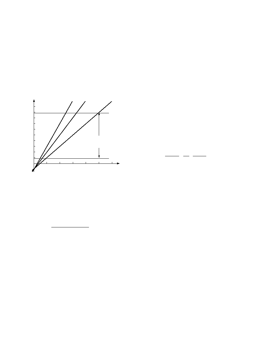
shows the ideal gain curves for a nominal preamplifier gain of
14 dB which are described by the following equations:
G (20 dB/V) = 20
×
VGN 5, V
REF
= 2.500 V
(4)
G (30 dB/V) = 30
×
VGN 5, V
REF
= 1.666 V
(5)
G (40 dB/V) = 40
×
VGN 5, V
REF
= 1.250 V
(6)
GAIN CONTROL VOLTAGE VGN
20
40
35
30
25
15
10
5
50
45
0
5
LINEAR-IN-dB RANGE
OF AD604 WITH
PREAMPLIFIER
SET TO 14dB
0.5
1.0
2.5
1.5
2.0
3.0
GAIN dB
30dB/V
40dB/V
20dB/V
Figure 40. Ideal Gain Curves vs. V
REF
.
From these equations you can see that all gain curves intercept
at the same 5 dB point; this intercept will be 6 dB higher
(+1 dB) if the preamplifier gain is set to +20 dB or 14 dB,
lower (19 dB) if the preamplifier is not used at all. Outside of
the central linear range, the gain starts to deviate from the ideal
control law but still provides another 8.4 dB of range. For a given
gain scaling you can calculate V
REF
as shown in Equation 7:
V
REF
=
2.500 V
×
20 dB / V
Gain Scale
(7)
Usable gain control voltage ranges are 0.1 V to 2.9 V for
20 dB/V scale and 0.1 V to 1.45 V for the 40 dB/V scale. VGN
voltages of less than 0.1 V are not used for gain control since
below 50 mV the channel (preamp and DSX) is powered down.
This can be used to conserve power and at the same time gate-
off the signal. The supply current for a powered-down channel
is 1.9 mA, the response time to power the device on-or-off, is
less than 1
µ
s.
Active Feedback Amplifier (Fixed Gain Amp)
To achieve single supply operation and a fully differential input
to the DSX, an active-feedback amplifier (AFA) is utilized. The
AFA is basically an op amp with two g
m
stages; one of the active
stages is used in the feedback path (therefore the name), while
the other is used as a differential input. Note that the differential
input is an open-loop gm stage that requires that it be highly
linear over the expected input signal range. In this design, the
g
m
stage that senses the voltages on the attenuator is a distrib-
uted one; for example, there are as many g
m
stages as there are
taps on the ladder network. Only a few of them are on at any
one time, depending on the gain-control voltage.
The AFA makes a differential input structure possible since one
of its inputs (G1) is fully differential; this input is made up of a
distributed g
m
stage. The second input (G2) is used for feed-
back. The output of G1 will be some function of the voltages
sensed on the attenuator taps which is applied to a high gain
amplifier (A0). Because of negative feedback, the differential
input to the high gain amplifier has to be zero; this in turn
implies that the differential input voltage to G2 times g
m2
(the
transconductance of G2) has to be equal to the differential input
voltage to G1 times g
m1
(the transconductance of G1). There-
fore the overall gain function of the AFA is:
V
OUT
V
ATTEN
=
g
m1
g
m2
×
R1
+
R2
R2
(8)
where V
OUT
is the output voltage, V
ATTEN
is the effective voltage
sensed on the attenuator, (R1+R2)/R2 = 42, and g
m1
/g
m2
=
1.25; the overall gain is thus 52.5 (34.4 dB).
The AFA has additional features: (1) inverting the signal by
switching the positive and negative input to the ladder network,
(2) the possibility of using the DSX1 input as a second signal
input, (3) fully differential high impedance inputs when both
preamplifiers are used with one DSX (the other DSX could still
be used alone), and (4) independent control of the DSX common-
mode voltage. Under normal operating conditions it is best to
connect a decoupling capacitor to pin VOCM in which case the
common-mode voltage of the DSX is half the supply voltage;
this allows for maximum signal swing. Nevertheless, the
common-mode voltage can be shifted up or down by directly
applying a voltage to VOCM. It can also be used as another
signal input, the only limitation being the rather low slew-rate
of the VOCM buffer.
If the dc level of the output signal is not critical, another
coupling capacitor is normally used at the output of the DSX;
again this is done for level shifting and to eliminate any dc off-
sets contributed by the DSX (see AC Coupling section).
AD604
REV. 0
13
APPLICATIONS
The most basic circuit in Figure 41 shows the connections for
one channel of the AD604. The signal is applied at Pin 5. RGN
is normally zero, in which case the preamplifier is set to a gain-
of-five (14 dB). When Pin FBK1 is left open, the preamplifier is
set to a gain-of-ten (20 dB) and the gain range shifts up by
6 dB. The ac coupling capacitors before pins DSX1 and
+DSX1 should be selected according to the required lower cut-
off frequency. In this example the 0.1
µ
F capacitors together
with the 175
seen looking into each of the DSX input pins,
provides a 3 dB high pass corner of about 9.1 kHz. The upper
cutoff frequency is determined by the bandwidth of the channel
which is 40 MHz. Note, the signal can be simply inverted by
connecting the output of the preamplifier to pin DSX1 instead
of +DSX1, this is due to the fully differential input of the DSX.
12
11
10
9
8
1
2
3
4
7
6
5
13
16
15
14
24
23
22
21
20
19
18
17
AD604
V
IN
VGN
RGN
0.1µF
0.1µF
2.500V
0.1µF
0.1µF
R
L
500
+5V
5V
OUT
DSX1
+DSX1
PAI1
FBK1
PAO1
COM1
COM2
PAI2
FBK2
PAO2
+DSX2
DSX2
VGN1
VREF
VPOS
GND1
OUT1
VNEG
VNEG
VPOS
GND2
OUT2
VOCM
VGN2
Figure 41. Basic Connections for a Single Channel
As shown here, the output is ac coupled for optimum perfor-
mance. In the case of connecting to the AD9050, ac coupling
can be eliminated as long as pin VOCM is biased by the same
3.3 V common-mode voltage as the AD9050 (see Figure 50).
Pin V
REF
requires a voltage of 1.25 V to 2.5 V, with between
40 dB/V and 20 dB/V gain scaling respectively. Voltage VGN
controls the gain; its nominal operating range is from 0.25 V to
2.65 V for 20 dB/V gain scaling, and 0.125 V to 1.325 V for
40 dB/V scaling. When this pin is taken to ground, the chan-
nel will power down and disable its output.
Pin COM1 is the main signal ground for the preamplifier and
needs to be connected with as short a connection as possible to
the input ground. Since the internal feedback resistors of the
preamplifier are very small for noise reasons (8
and 32
nominally), it is of utmost importance to keep the resistance in
this connection to a minimum! Furthermore, excessive induc-
tance in this connection may lead to oscillations.
As a consequence of the AD604's ultralow noise and wide band-
width, large dynamic currents will be flowing to and from the
power supply. To insure the stability of the part, extreme atten-
tion to supply decoupling is required. A large storage capacitor
in parallel with a smaller high frequency capacitor connected
right at the supply pins, together with a ferrite bead coming from
the supply should be used to insure high frequency stability.
To provide for additional flexibility, Pin COM1 can be used to
depower the preamplifier. When COM1 is connected to VP,
the preamplifier will be off, yet the DSX portion can be used
independently. This may be of value when one desires to cas-
cade the two DSX stages in the AD604. In this case the first
DSX output signal with respect to noise will be large and using
the second preamplifier at this point would be a waste of power
(see AGC Amplifier Application).
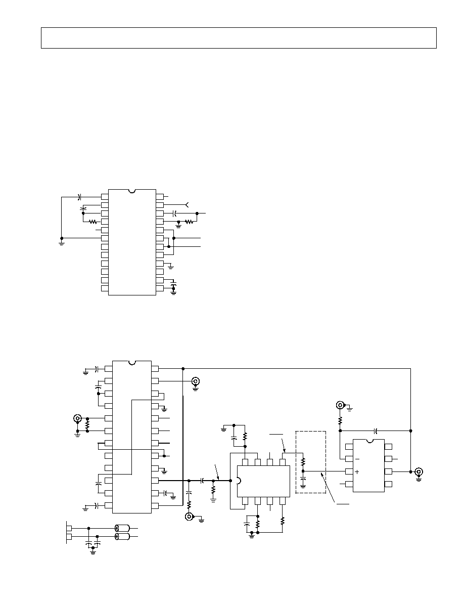
An Ultralow Noise AGC Amplifier with 82 to 96 dB Gain
Range
Figure 42 shows an implementation of an AGC amplifier with
82 dB of gain range using a single AD604. First, the connec-
tions for the two channels of the AD604 will be discussed, and
second, how the detector circuitry that closes the loop works.
VG
13
16
15
14
19
18
17
24
23
22
21
20
12
11
10
9
8
1
2
3
4
7
6
5
AD604
5V
+5V
C3
0.1µF
C11
1µF
VIN
VREF
C4
0.1µF
C7
0.1µF
R2
453
C2
0.1µF
RF OUT
C1
0.1µF
R1
49.9
5V
+5V
(MAX
800mV p-p)
8
7
6
5
1
2
3
4
AD711
OFFS
NULL
VS
NC
+VS
OFFS
NULL
OUT
C6
0.56µF
C7
0.33µF
R3
1k
V1 = V
IN
* G
8
7
6
5
1
2
3
4
Y1
Y2
VN
Z
X1
X2
VP
W
AD835
R4
2k
C8
0.33µF
+5V
(V1)
2
1V
5V
R5
2k
C9
0.33µF
R6
2k
R7
1k
C10
1µF
LOW
PASS
FILTER
5V
+5V
(A)
2
2
IF V1 = A*cos (wt)
R8
2k
VSET (
<
0V)
DSX1
+DSX1
PAI1
FBK1
PAO1
COM1
COM2
PAI2
FBK2
PAO2
+DSX2
DSX2
VGN1
VREF
VPOS
GND1
OUT1
VNEG
VNEG
VPOS
GND2
OUT2
VOCM
VGN2
C12
0.1µF
FB
FB
C13
0.1µF
+5V
5V
ALL SUPPLY PINS ARE DECOUPLED AS SHOWN.
Figure 42. AGC Amplifier with 82 dB of Gain Range
AD604
REV. 0
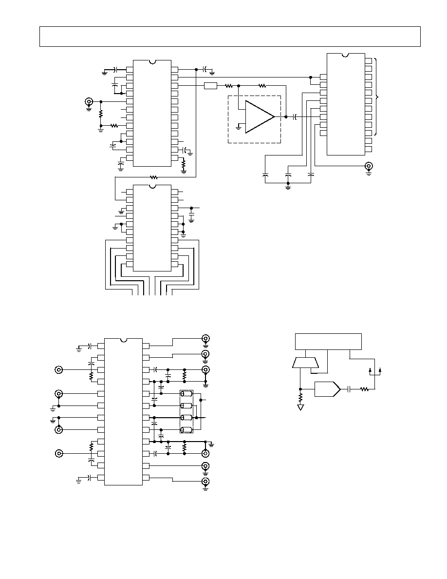
14
The signal is applied to connector VIN, and since the signal
source was 50
, a terminating resistor (R1) of 50
was added.
The signal is then amplified by 14 dB (Pin FBK1 shorted to
PAO1) through the Channel 1 preamplifier, and is further pro-
cessed by the Channel 1 DSX. Next the signal is applied directly
to the Channel 2 DSX. The second preamplifier is powered
down by connecting its COM2 pin to the positive supply as
explained in the preamplifier section earlier. Capacitors C1 and
C2 level shift the signal from the preamplifier into the first DSX
and at the same time eliminate any offset contribution of the
preamp. C3 and C4 have the same offset cancellation purpose
for the second DSX. Each set of capacitors together with the
175
input resistance of the corresponding DSX provides a
high pass filter with 3 dB corner frequency of about 9.1 kHz.
Pin VOCM is decoupled to ground by a 0.1
µ
F capacitor, while
VREF can be externally provided; in this application the gain
scale is set to 20 dB/V by applying 2.500 V. Since each of the
DSX amplifiers operates from a single +5 V supply, the output
is ac coupled via C6 and C7. The output signal can be moni-
tored at the connector labeled RF OUT.
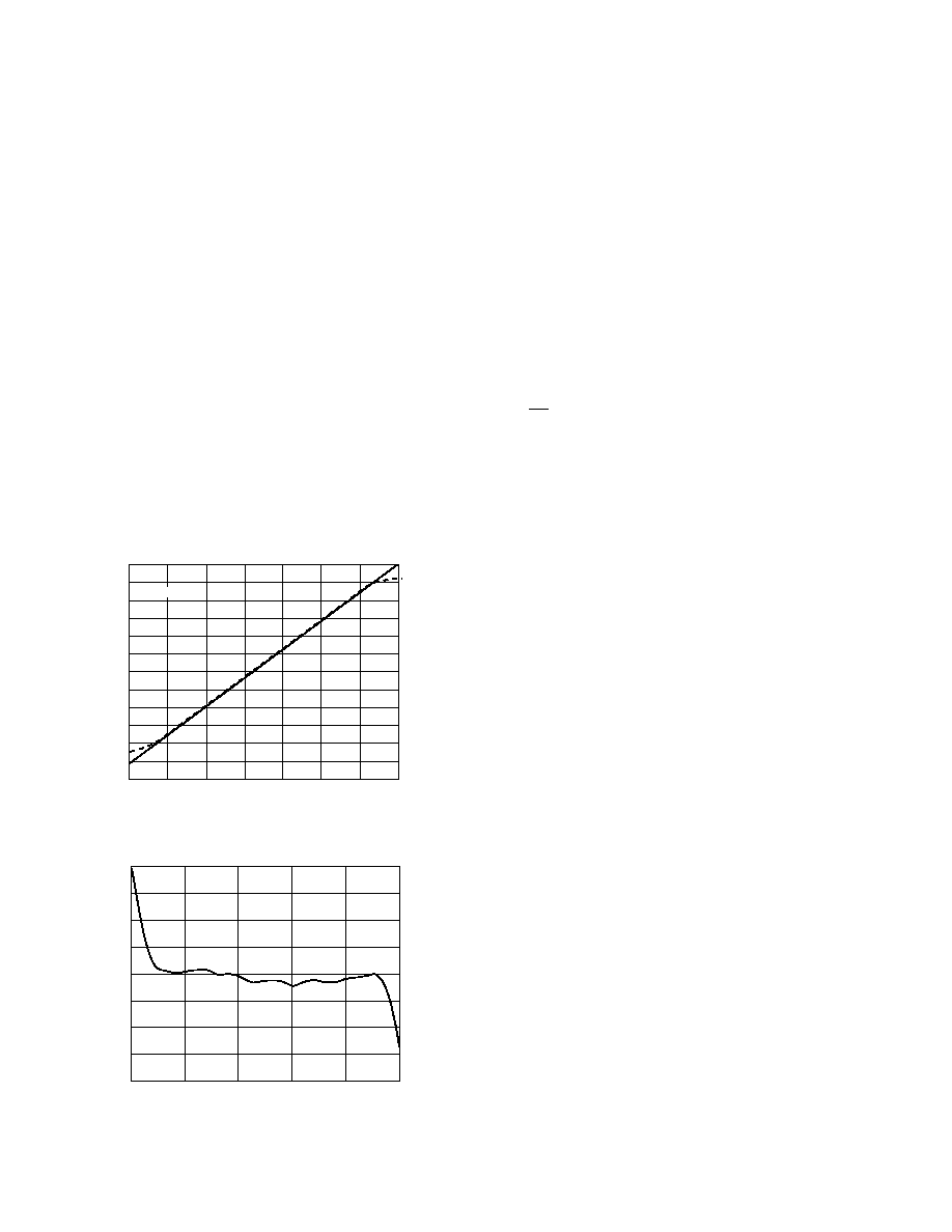
Figures 43 and 44 show the gain range and gain error for the
AD604 connected as shown. The gain range is 14 dB to +82 dB;
the useful range is 0 dB to +82 dB if the RF output amplitude is
controlled to
±
400 mV (+2 dBm). The main limitation on the
lower end of the signal range is the input capability of the
VGN Volts
90
80
30
70
60
20
50
40
30
20
10
0
10
1.7
0.1
0.5
0.9
1.3
2.1
2.5
2.9
GAIN dB
f = 1MHz
Figure 43. AD604 Cascaded Gain vs. VGN
VGN Volts
4
3
4
2.2
2
1
3
0
1
2
0.2
0.7
1.2
1.7
2.7
GAIN ERROR dB
f = 1MHz
Figure 44. AD604 Cascaded Gain Error vs. VGN
preamplifier. This can be overcome by adding an attenuator in
front of the preamplifier, but that would defeat the advantage of
the ultralow noise preamplifier. It should be noted that the sec-
ond preamplifier is not used since its ultralow noise and the
associated high power consumption are overkill after the first
DSX stage. It is disabled in this application by connecting the
COM2 pin to the positive supply. Nevertheless, the second
preamplifier can be used if so desired and the useful gain range
will shift up by 14 dB, to encompass 0 dB to +96 dB of gain.
For the same +2 dBm output this would allow signals as small
as 94 dBm to be measured.
To achieve the highest gains, the input signal has to ultimately
be bandlimited to reduce the noise; this is especially true if the
second preamplifier is used. If the maximum signal at Pin OUT2
of the AD604 is limited to be
±
400 mV (+2 dBm), then the in-
put signal level at the AGC threshold is 25
µ
V rms (79 dBm).
The circuit as shown has about 40 MHz of noise bandwidth; the
0.8 nV/
Hz
of input referred voltage noise spectral density of
the AD604 results in an rms noise of 5.05
µ
V in the 40 MHz
bandwidth. The 50
termination resistor, together with the
50
source resistance of the signal generator, combine to an
effective resistance as seen by the input of the preamplifier of
25
which makes 4.07
µ
V of rms noise in 40 MHz. The noise
floor of this channel is consequently the rms sum of these two
main noise sources, 6.5
µ
V rms. This means that the minimum
dectectable signal (MDS) for this circuit is 6.5
µ
V rms
(90.7 dBm). As a general rule of thumb the measured signal
should be about a factor-of-three larger than the noise floor, in
this case 19.5
µ
V rms. As we can see the 25
µ
V rms signal that
this AGC circuit can correct for is just slightly above the MDS.
Of course, the sensitivity of the input can be improved by
bandlimiting the signal; if the noise bandwidth is reduced by a
factor-of-four to 10 MHz, the noise floor of the AGC circuit
with 50
termination resistor will drop to 3.25
µ
V rms
(96.7 dBm). Further noise improvement can be achieved by an
input matching network or by transformer coupling of the input
signal.
Next we will describe the functioning of the detector circuitry
comprised of a squarer, a low-pass filter, and an integrator. At
this point it is necessary to make some assumptions about the
input signal. The following explanation of the detector circuitry
presumes an amplitude modulated RF carrier where the modu-
lating signal is at a much lower frequency than the RF signal.
The AD835 multiplier functions as the detector by squaring the
output signal presented to it by the AD604. A low-pass filter fol-
lowing the squaring operation removes the RF signal component
at twice the incoming signal frequency, while passing the low
frequency AM information. The following integrator with a time
constant of 2 ms set by R8 and C11 integrates the error signal
presented by the low-pass filter and changes VG until the error
signal is equal to V
SET
.
For example, if the signal presented to the detector is V1 =
A*cos(
t) as indicated in Figure 42, then the output of the
squarer is (V1)
2
/1 V. The reason for all the minus signs in the
detection circuitry comes from the necessity of providing nega-
tive feedback in the control loop; actually if V
SET
becomes
greater-than 0 V, the control loop provides positive feedback.
Squaring A*cos(
t) results in two terms, one at dc and one at
2
; the following low-pass filter passes only the (A)
2
/2 dc term.
AD604
REV. 0
15
This dc voltage will now be forced equal to the voltage, V
SET
, by
the control loop. The squarer together with the low-pass filter
functions as a mean-square detector. As should be evident, by
controlling the value of V
SET
, we can set the amplitude of the
voltage V1 at the input of the AD835; if V
SET
equals minus
80 mV, the AGC output signal amplitude will be
±
400 mV.
Figure 45 shows the control voltage, VGN, versus the input
power at frequencies of 1 MHz (solid line) and 10 MHz (dashed
line) at an output regulated level of +2 dBm (800 mV p-p). The
AGC threshold is evident at a P
IN
of about 79 dBm; the high-
est input power that could still be accommodated was about
+3 dBm. At this level the output starts being distorted because
of clipping in the preamplifier.
P
IN
dBm
4.5
4.0
0.5
0
40
3.5
3.0
1.0
2.5
2.0
1.5
80
70
60
50
30
20
10
10
CONTROL VOLTAGE Volts
1MHz
10MHz
Figure 45. Control Voltage vs. Input Power of Circuit in
Figure 42
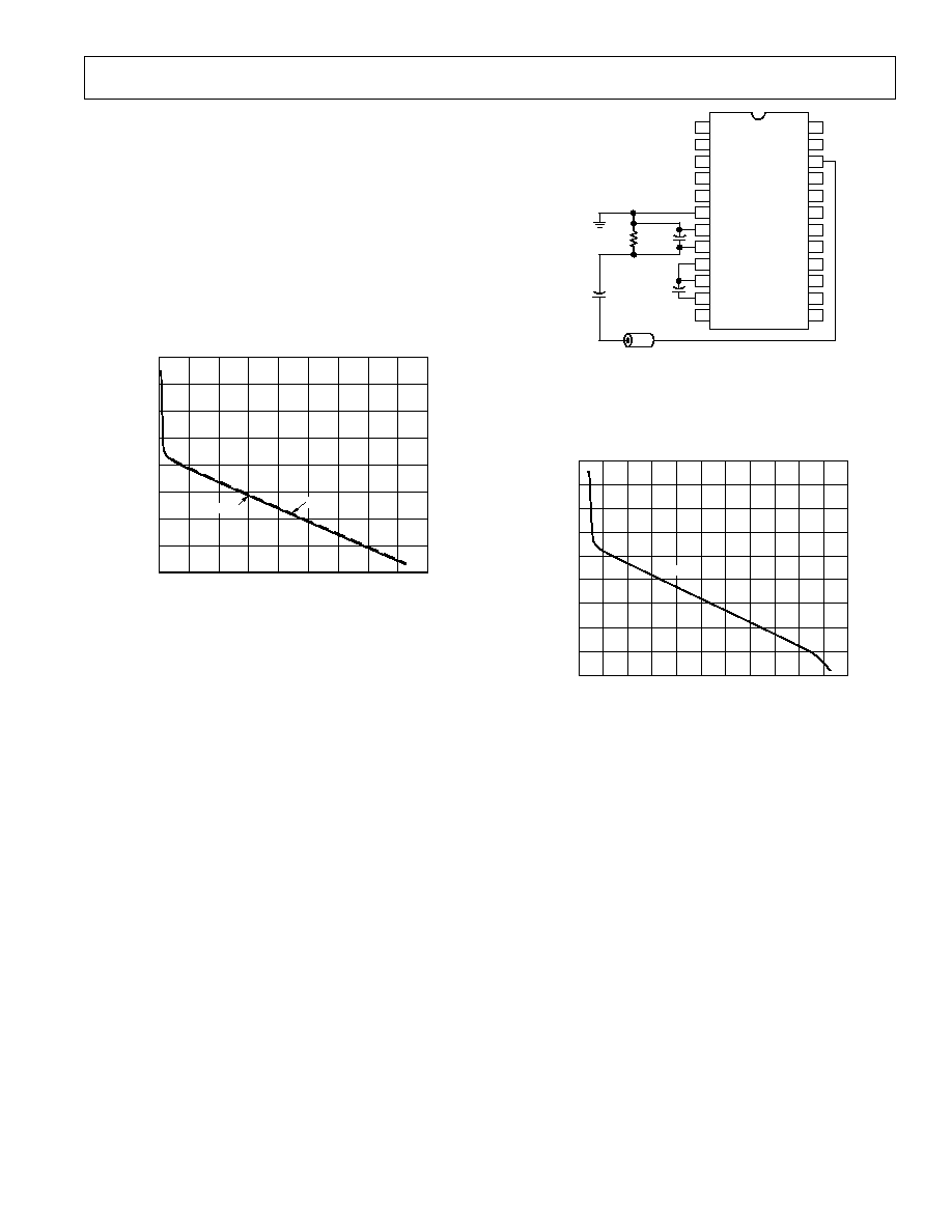
As mentioned already, the second preamplifier can be used to
extend the range of the AGC circuit in Figure 42. Figure 46
shows the modifications that need to be made to Figure 44 to
achieve 96 dB of gain and dynamic range. Because of the ex-
tremely high gain, the bandwidth needs to be limited to reject
some of the noise; furthermore, limiting the bandwidth will help
suppress high frequency oscillations. The added components act
as a low-pass filter and dc block (C5 level shifts the output of
the first DSX from 2.5 V to ground); the ferrite bead has an im-
pedance of about 5
at 1 MHz, 30
at 10 MHz, and 70
at
100 MHz. Together with R2 and C6, the bead makes a low-pass
filter which attenuates higher frequencies; at 1 MHz the attenu-
ation is about 0.2 dB, while at 10 MHz it increases to 6 dB, on
to 28 dB at 100 MHz. Signals now have to be less than about
1 MHz to not be significantly affected by the added circuitry.
In Figure 47 we see the control voltage vs. input power at
1 MHz to the circuit in Figure 46; note that the AGC threshold
is at 95 dBm. The output signal level was set to 800 mV p-p by
applying 80 mV to the V
SET
connector.
12
11
10
9
8
1
2
3
4
7
6
5
13
16
15
14
24
23
22
21
20
19
18
17
AD604
C3
0.1µF
R2
499
C6
560pF
FB
C5
0.1µF
FAIR-RITE
#2643000301
DSX1
+DSX1
PAI1
FBK1
PAO1
COM1
COM2
PAI2
FBK2
PAO2
+DSX2
DSX2
VGN1
VREF
VPOS
GND1
OUT1
VNEG
VNEG
VPOS
GND2
OUT2
VOCM
VGN2
Figure 46. Modifications of AGC Amplifier to Get 96 dB of
Gain Range
P
IN
dBm
4.5
4.0
0
100
0
40
3.5
3.0
1.0
2.5
2.0
1.5
90
80
70
60
50
30
20
10
10
CONTROL VOLTAGE Volts
1MHz
0.5
Figure 47. Control Voltage vs. Input Power of Circuit in
Figure 46
AD604
REV. 0
16
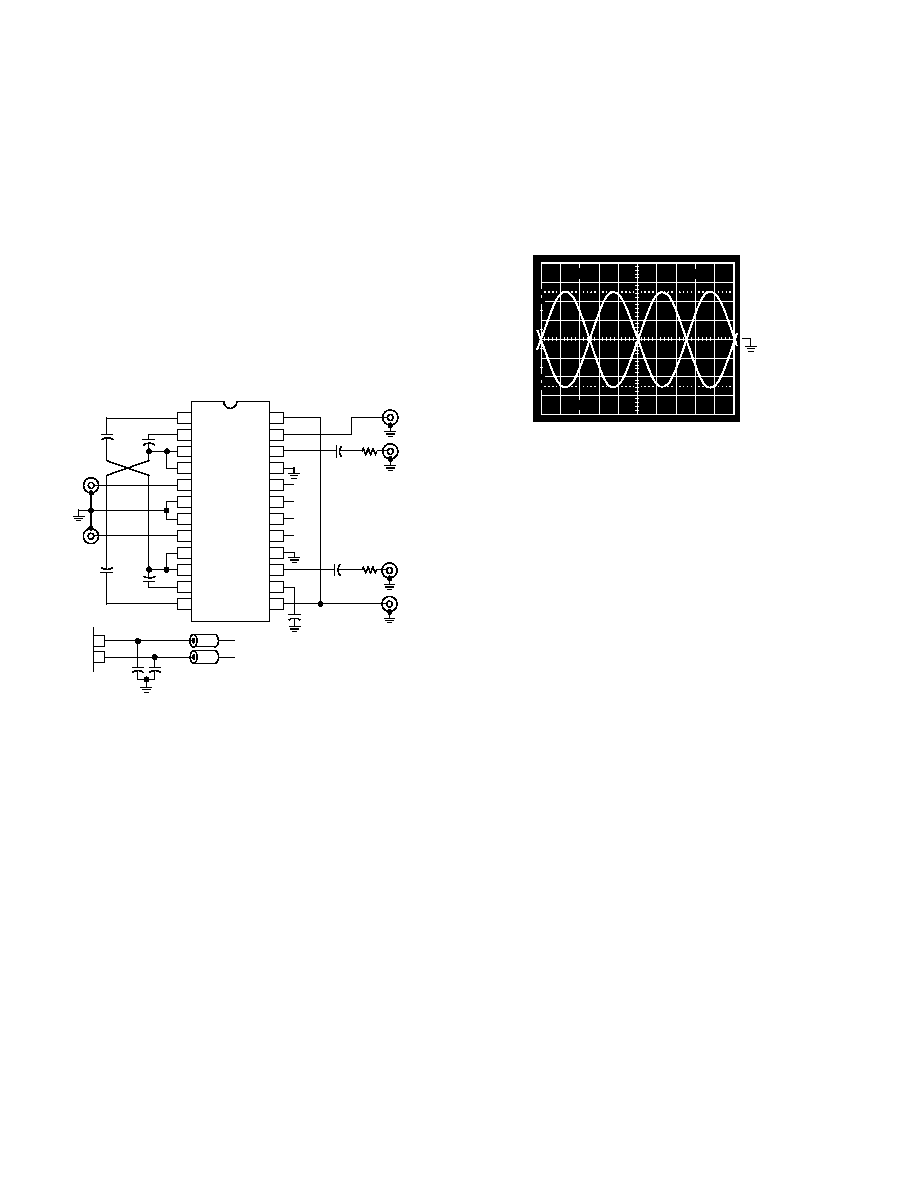
Ultralow Noise, Differential Input-Differential Output VGA
Figure 48 shows how to use both preamplifiers and DSXs to
create a high impedance, differential input-differential output
variable gain amplifier. This application takes advantage of the
differential inputs to the DSXs. It should be pointed out that
the input is not truly differential, in the sense that the common-
mode voltage needs to be at ground to achieve maximum input
signal swing. This has mainly to do with the limited output
swing capability of the output drivers of the preamplifiers; they
clip around
±
2.2 V due to having to drive an effective load of
about 30
. If a different input common-mode voltage needs to
be accommodated, ac coupling (as was done in Figure 46) is
recommended. The differential gain range of this circuit runs
from +6 dB to +54 dB. This is 6 dB higher than each individual
channel of the AD604 because the DSX inputs now see twice
the signal amplitude compared to when they are driven single
ended.
13
16
15
14
19
18
17
24
23
22
21
20
12
11
10
9
8
1
2
3
4
7
6
5
AD604
C3
0.1µF
C12
0.1µF
FB
FB
C13
0.1µF
+5V
5V
ALL SUPPLY PINS ARE DECOUPLED AS SHOWN.
C4
0.1µF
C2
0.1µF
R2
453
+5V
5V
5V
+5V
C5
0.1µF
C6
0.1µF
R1
453
C7
0.1µF
C1
0.1µF
VIN+
VIN
VG
VREF
VOUT+
VOUT
DSX1
+DSX1
PAI1
FBK1
PAO1
COM1
COM2
PAI2
FBK2
PAO2
+DSX2
DSX2
VGN1
VREF
VPOS
GND1
OUT1
VNEG
VNEG
VPOS
GND2
OUT2
VOCM
VGN2
Figure 48. Ultralow Noise, Differential InputDifferential
Output VGA
Figure 49 displays the output signals VOUT+ and VOUT after
a 20 dB attenuator formed between the 453
resistors shown
in Figure 48 and the 50
loads presented by the oscilloscope
plug-in. R1 and R2 were inserted to insure a nominal load of
500
at each output. The differential gain of the circuit was set
to +20 dB by applying a control voltage, VGN, of 1 V; the gain
scaling was 20 dB/V for a VREF of 2.500 V; the input frequency
was 10 MHz and the differential input amplitude 100 mV p-p.
The resulting differential output amplitude was 1 V p-p as can
be seen on the scope photo when reading the vertical scale as
200 mV/div.
10
0%
100
90
20ns
20mV
20mV
+500mV
500mV
ACTUAL
V
OUT
NOTE 1. OUTPUT AFTER 10x ATTENUATER FORMED
BY 453
TOGETHER WITH 50
OF 7A24 PLUG-IN.
Figure 49. Output of VGA in Figure 48 for V
G
= 1 V
Medical Ultrasound TGC Driving the AD9050, a 10-Bit,
40 MSPS A/D
The AD604 is an ideal candidate for the TGC (Time Gain
Control) amplifier that is required in medical ultrasound sys-
tems to limit the dynamic range of the signal that is presented to
the A/D converter. Figure 50 shows a schematic of an AD604
driving an AD9050 in a typical medical ultrasound application.
The gain is controlled by means of a digital byte that is input to
an AD7226 D/A converter that outputs the analog gain control
signal. The output common-mode voltage of the AD604 is set
to VPOS/2 by means of an internal voltage divider. The VOCM
pin is bypassed with a 0.1
µ
F to ground.
The DSX output is optionally filtered and then buffered by an
AD9631 op amp, a low distortion, low noise amplifier. The op
amp output is ac coupled into the self-biasing input of an
AD9050 A/D converter which is capable of outputting 10 bits at
a 40 MSPS sampling rate.
AD604
REV. 0
17
20
27
28
15
16
17
18
19
24
25
26
22
14
13
10
3
4
9
6
5
AD9050
COMP
VREF
IN
VREF
OUT
REF
BP
AINB
ENCODE
OR
AIN
(MSB) D9
D8
D5
D6
D7
D4
D3
D2
D1
(LSB) D0
+5V
+5V
A/D
OUTPUT
13
16
15
14
24
23
22
21
20
19
18
17
12
11
10
9
8
1
2
3
4
7
6
5
AD604
0.1µF
0.1µF
0.1µF
1k
0.1µF
50
CLK
0.1µF
50
J2
ANALOG
INPUT
100
12
11
20
19
18
17
16
15
14
13
10
9
8
1
2
3
4
7
6
5
AD7226
V
OUT
B
V
OUT
A
AGND
V
REF
V
SS
DGND
DB7
(MSB)
DB6
DB5
DB4
V
OUT
C
V
OUT
D
A1
A0
V
DD
WR
DB0
(LSB)
DB1
DB2
DB3
VREF
+15V
DIGITAL GAIN CONTROL
0.1µF
FILTER
1k
2
3
6
AD9631
1k
OPTIONAL
0.1µF
0.1µF
0.1µF
0.1µF
IN
+IN
OUT
DSX1
+DSX1
PAI1
FBK1
PAO1
COM1
COM2
PAI2
FBK2
PAO2
+DSX2
DSX2
VGN1
VREF
VPOS
GND1
OUT1
VNEG
VNEG
VPOS
GND2
OUT2
VOCM
VGN2
Figure 50. TGC Circuit for Medical Ultrasound Application
AD604
DUT
0.1µF
450
PAI
49.9
OUT
R
A
HP3577B
50
HP11636B
POWER
SPLITTER
Figure 52. Setup for Gain Measurements
13
16
15
14
19
18
17
24
23
22
21
20
12
11
10
9
8
1
2
3
4
7
6
5
AD604
R1
500
+5V
5V
C6
0.1µF
C11
0.1µF
C4
0.1µF
IN1
VREF
OUT1
VOCM
C2
5pF
C12
0.1µF
R4
500
C10
0.1µF
C5
0.1µF
C8
5pF
C9
0.1µF
C7
0.1µF
VG1
VG2
OUT2
R3
RGN
C1
0.1µF
R2
RGN
NOTE 2
NOTE 3
NOTE 3
IN2
PAO2
PAO1
C3
0.1µF
NOTES:
1. PAO1 AND PAO2 ARE USED TO MEASURE PREAMPS.
2. RGN = 0 NOMINALLY; PREAMP GAIN = 5, RGN = OPEN; PREAMP GAIN = 10
3. WHEN MEASURING BW WITH 50
SPECTRUM ANALYZER, USE 450
IN SERIES.
DSX1
+DSX1
PAI1
FBK1
PAO1
COM1
COM2
PAI2
FBK2
PAO2
+DSX2
DSX2
VGN1
VREF
VPOS
GND1
OUT1
VNEG
VNEG
VPOS
GND2
OUT2
VOCM
VGN2
OPTIONAL
Figure 51. Basic Test Board
AD604
REV. 0
18
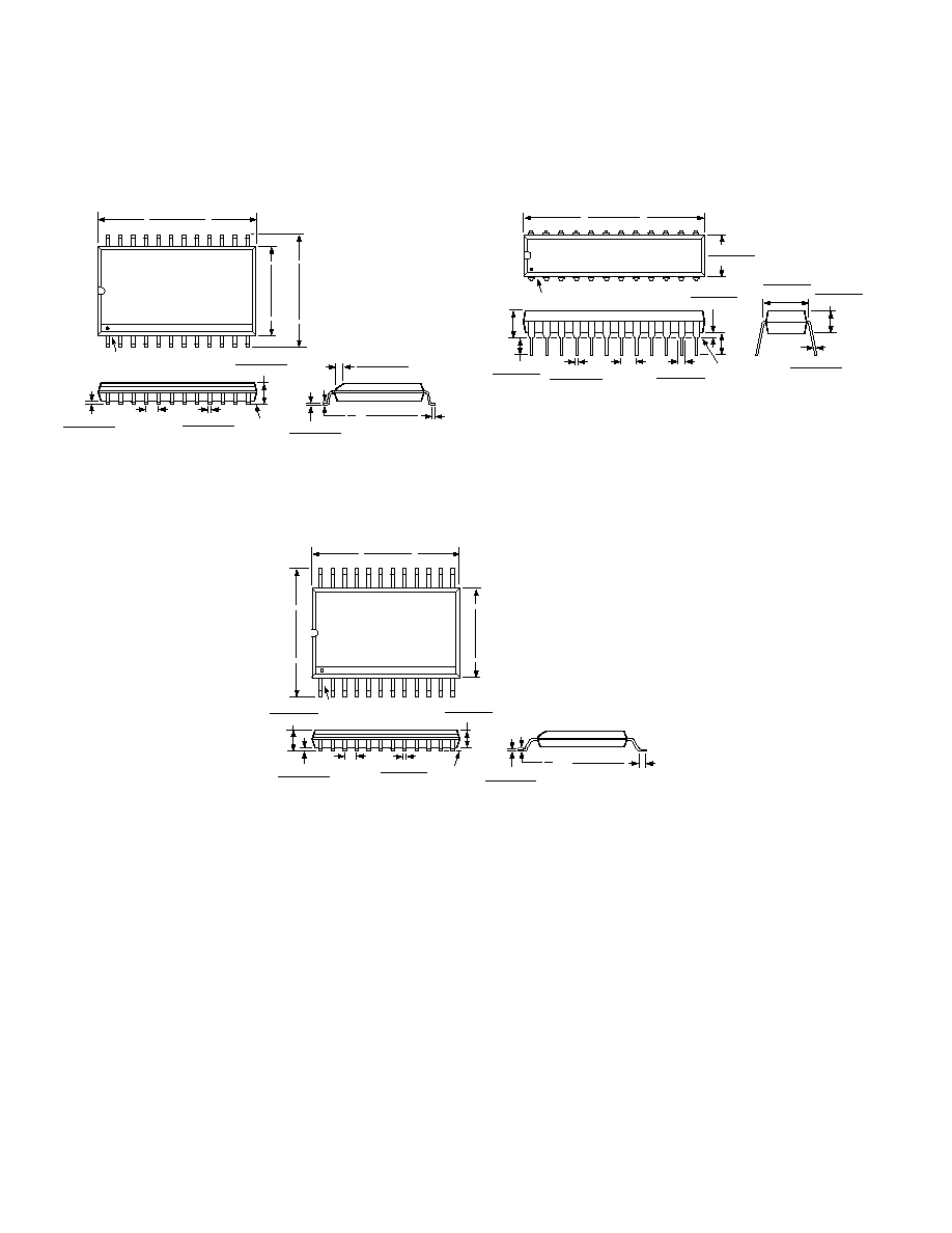
OUTLINE DIMENSIONS
Dimensions shown in inches and (mm).
Small Outline IC Package
(R-24)
24
13
12
1
0.6141 (15.60)
0.5985 (15.20)
0.4193 (10.65)
0.3937 (10.00)
0.2992 (7.60)
0.2914 (7.40)
PIN 1
SEATING
PLANE
0.0118 (0.30)
0.0040 (0.10)
0.0192 (0.49)
0.0138 (0.35)
0.1043 (2.65)
0.0926 (2.35)
0.0500
(1.27)
BSC
0.0125 (0.32)
0.0091 (0.23)
0.0500 (1.27)
0.0157 (0.40)
8
°
0
°
0.0291 (0.74)
0.0098 (0.25)
x 45
°
Plastic DIP Package
(N-24)
24
1
12
13
1.275 (32.30)
1.125 (28.60)
0.280 (7.11)
0.240 (6.10)
PIN 1
SEATING
PLANE
0.022 (0.558)
0.014 (0.356)
0.060 (1.52)
0.015 (0.38)
0.150
(3.81)
MIN
0.070 (1.77)
0.045 (1.15)
0.200 (5.05)
0.125 (3.18)
0.210
(5.33)
MAX
0.100
(2.54)
BSC
0.325 (8.25)
0.300 (7.62)
0.015 (0.381)
0.008 (0.204)
0.195 (4.95)
0.115 (2.93)
Shrink Small Outline Package
(RS-24)
24
1
13
12
0.328 (8.33)
0.318 (8.08)
0.311 (7.9)
0.301 (7.64)
0.212 (5.38)
0.205 (5.207)
PIN 1
SEATING
PLANE
0.008 (0.203)
0.002 (0.050)
0.07 (1.78)
0.066 (1.67)
0.0256
(0.65)
BSC
0.078 (1.98)
0.068 (1.73)
0.015 (0.38)
0.010 (0.25)
0.009 (0.229)
0.005 (0.127)
0.037 (0.94)
0.022 (0.559)
8
°
0
°

19

C2190910/96
PRINTED IN U.S.A.
20