 | ÐлекÑÑоннÑй компоненÑ: AD608AR | СкаÑаÑÑ:  PDF PDF  ZIP ZIP |
Äîêóìåíòàöèÿ è îïèñàíèÿ www.docs.chipfind.ru
a
Low Power Mixer/Limiter/RSSI
3 V Receiver IF Subsystem
AD608
© Analog Devices, Inc., 1996
One Technology Way, P.O. Box 9106, Norwood, MA 02062-9106, U.S.A.
Tel: 617/329-4700
Fax: 617/326-8703
FEATURES
Mixer
15 dBm 1 dB Compression Point
5 dBm IP3
24 dB Conversion Gain
>500 MHz Input Bandwidth
Logarithmic/Limiting Amplifier
80 dB RSSI Range
3 Phase Stability over 80 dB Range
Low Power
21 mW at 3 V Power Consumption
CMOS-Compatible Power-Down to 300 W typ
200 ns Enable/Disable Time
APPLICATIONS
PHS, GSM, TDMA, FM, or PM Receivers
Battery-Powered Instrumentation
Base Station RSSI Measurement
The RF and LO bandwidths both exceed 500 MHz. In a typical
IF application, the AD608 will accept the output of a 240 MHz
SAW filter and downconvert it to a nominal 10.7 MHz IF with
a conversion gain of 24 dB (Z
IF
= 165
). The AD608's loga-
rithmic/limiting amplifier section handles any IF from LF to as
high as 30 MHz.
The mixer is a doubly-balanced "Gilbert-Cell" type and oper-
ates linearly for RF inputs spanning 95 dBm to 15 dBm. It
has a nominal 5 dBm third-order intercept. An onboard LO
preamplifier requires only 16 dBm of LO drive. The mixer's
current output drives a reverse-terminated, industry-standard
10.7 MHz 330
filter.
The nominal logarithmic scaling is such that the output is
+0.2 V for a sinusoidal input to the IF amplifier of 75 dBm
and +1.8 V at an input of +5 dBm; over this range the logarith-
mic conformance is typically
±
1 dB. The logarithmic slope is
proportional to the supply voltage. A feedback loop automati-
cally nulls the input offset of the first stage down to the sub-
microvolt level.
The AD608's limiter output provides a hard-limited signal out-
put at 400 mV p-p. The voltage gain of the limiting amplifier to
this output is more than 100 dB. Transition times are 11 ns and
the phase is stable to within
±
3
°
at 10.7 MHz for signals from
75 dBm to +5 dBm.
The AD608 is enabled by a CMOS logic-level voltage input,
with a response time of 200 ns. When disabled, the standby
power is reduced to 300
µ
W within 400 ns.
The AD608 is specified for the industrial temperature range of
25
°
C to +85
°
C for 2.7 V to 5.5 V supplies and 40
°
C to +85
°
C
for 4.5 V to 5.5 V supplies. It comes in a 16-pin plastic SOIC.
GENERAL DESCRIPTION
The AD608 provides both a low power, low distortion, low
noise mixer and a complete, monolithic logarithmic/limiting
amplifier using a "successive-detection" technique. It provides
both a high speed RSSI (Received Signal Strength Indicator)
output with 80 dB dynamic range and a hard-limited output.
The RSSI output is from a two-pole post-demodulation low-
pass filter and provides a loadable output voltage of +0.2 V to
+1.8 V. The AD608 operates from a single 2.7 V to 5.5 V sup-
ply at a typical power level of 21 mW at 3 V.
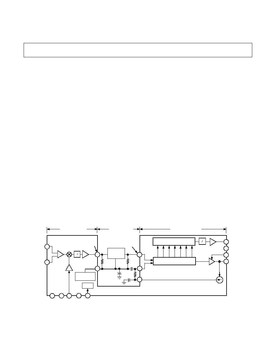
FUNCTIONAL BLOCK DIAGRAM
24dB MIXER GAIN
110dB LIMITER GAIN
90dB RSSI
BIAS
MXOP
MIXER
BPF
DRIVER
VMID
LO
PREAMP
AD608
RFHI
RFLO
IF INPUT
75dBm TO
+15dBm
2
IFHI
IFLO
LMOP
VPS2
RSSI
FDBK
COM3
FINAL
LIMITER
100nF
10nF
330
±
50µA
330
MID-SUPPLY
IF BIAS
5
7
8
10
9
13
14
12
11
2
4
16
LIMITER
OUTPUT
400mVp-p
PRUP
RF INPUT
95 TO
15dBm
1
VPS1 COM1
COM2
LOHI
RSSI OUTPUT
20mV/dB
0.2V TO 1.8V
3dB NOMINAL
INSERTION LOSS
+2.7V TO 5.5V
5-STAGE IF AMPLIFIER
(16dB PER STAGE)
7 FULL-WAVE
RECTIFIER CELLS
+2.7V TO
5.5V
LO INPUT
16dBm
CMOS LOGIC
INPUT
±
6mA MAX OUTPUT
(
±
890mV INTO 165
)
100
18nF
1
15dBm =
±
56mV MAX FOR LINEAR OPERATION
2MHz
LPF
15
1
3
6
2
39.76µV RMS TO 397.6mV RMS FOR
±
1dB RSSI
ACCURACY
NOTES:
10.7MHz
BANDPASS
FILTER
REV. B
Information furnished by Analog Devices is believed to be accurate and
reliable. However, no responsibility is assumed by Analog Devices for its
use, nor for any infringements of patents or other rights of third parties
which may result from its use. No license is granted by implication or
otherwise under any patent or patent rights of Analog Devices.

AD608SPECIFICATIONS
Model
AD608
Conditions
Min
Typ
Max
Units
MIXER PERFORMANCE
RF and LO Frequency Range
500
MHz
LO Power
Input Terminated in 50
16
dBm
Conversion Gain
Driving Doubly-Terminated 330
IF Filter, Z
IF
= 165
19
24
28
dB
Noise Figure
Matched Input, f
RF
= 100 MHz
11
dB
Matched Input, f
RF
= 240 MHz
16
dB
1 dB Compression Point
Input Terminated in 50
15
dBm
Third-Order Intercept
f
RF
= 240 MHz and 240.02 MHz, f
LO
= 229.3 MHz
5
dBm
Input Resistance
f
RF
= 100 MHz (See Table I)
1.9
k
Input Capacitance
f
RF
= 100 MHz (See Table I)
3
pF
LIMITER PERFORMANCE
Gain
Full Temperature and Supply Range
110
dB
Limiting Threshold
3
°
rms Phase Jitter at 10.7 MHz
75
dBm
280 kHz IF Bandwidth
Input Resistance
10
k
Input Capacitance
3
pF
Phase Variation
75 dBm to +5 dBm IF Input Signal at 10.7 MHz
±
3
Degree
DC Level
Center of Output Swing (VPOS-1)
2
V
Output Level
Limiter Output Driving 5 k
Load
400
mV p-p
Rise and Fall Times
Driving a 5 pF Load
11
ns
Output Impedance
200
RSSI PERFORMANCE
At 10.7 MHz
Nominal Slope
At VPOS = 3 V; Proportional to VPOS
17.27
20
23.27
mV/dB
Nominal Intercept
85
dBm
Minimum RSSI Voltage
75 dBm Input Signal
0.2
V
Maximum RSSI Voltage
+5 dBm Input Signal
1.8
V
RSSI Voltage Intercept
0 dBm Input Signal
1.57
1.82
V
Logarithmic Linearity Error
75 dBm to +5 dBm Input Signal at IFHI
±
1
dB
RSSI Response Time
90% RF to 50% RSSI
200
ns
Output Impedance
At Midscale
250
POWER-DOWN INTERFACE
Logical Threshold
System Active on Logical High
1.5
V
Input Current
For Logical High
75
µ
A
Power-Up Response Time
Active Limiter Output
200
ns
Power-Down Response Time
To 200
µ
A Supply Current
400
ns
Power-Down Current
100
µ
A
POWER SUPPLY
Operating Range
25
°
C to +85
°
C
2.7
5.5
V
40
°
C to +85
°
C
4.5
5.5
V
Powered Up Current
VPOS = 3 V
7.3
mA
OPERATING TEMPERATURE
T
MIN
to T
MAX
VPOS = 2.7 V to 5.5 V
25
+85
°
C
T
MIN
to T
MAX
VPOS = 4.5 V to 5.5 V
40
+85
°
C
Specifications subject to change without notice.
REV. B
2
(@ T
A
= + 25 C, Supply = 3 V, dBm is referred to 50 , unless otherwise noted)
AD608
REV. B
3
ABSOLUTE MAXIMUM RATINGS
1
Supply Voltage VPS1, VPS2 . . . . . . . . . . . . . . . . . . . . . . +6 V
Internal Power Dissipation
2
. . . . . . . . . . . . . . . . . . . . 600 mW
Temperature Range . . . . . . . . . . . . . . . . . . . . . 40
°
C to +85
°
C
Storage Temperature Range . . . . . . . . . . . . . 65
°
C to +150
°
C
Lead Temperature (Soldering 60 sec) . . . . . . . . . . . . . +300
°
C
NOTES
1
Stresses above those listed under "Absolute Maximum Ratings" may cause
permanent damage to the device. This is a stress rating only, and functional
operation of the device at these or any other conditions above those indicated in the
operational section of this specification is not implied. Exposure to absolute
maximum rating conditions for extended rating conditions for extended periods
may affect device reliability.
2
Thermal Characteristics:
16-Pin SOIC Package:
JA
= 110
°
C/W.
ORDERING GUIDE
Temperature
Package
Model
Range
Option
AD608AR
25
°
C to +85
°
C,
R-16A*
2.7 V to 5.5 V Supplies;
40
°
C to +85
°
C,
4.5 V to 5.5 V Supplies
*R = Small Outline IC (SOIC).
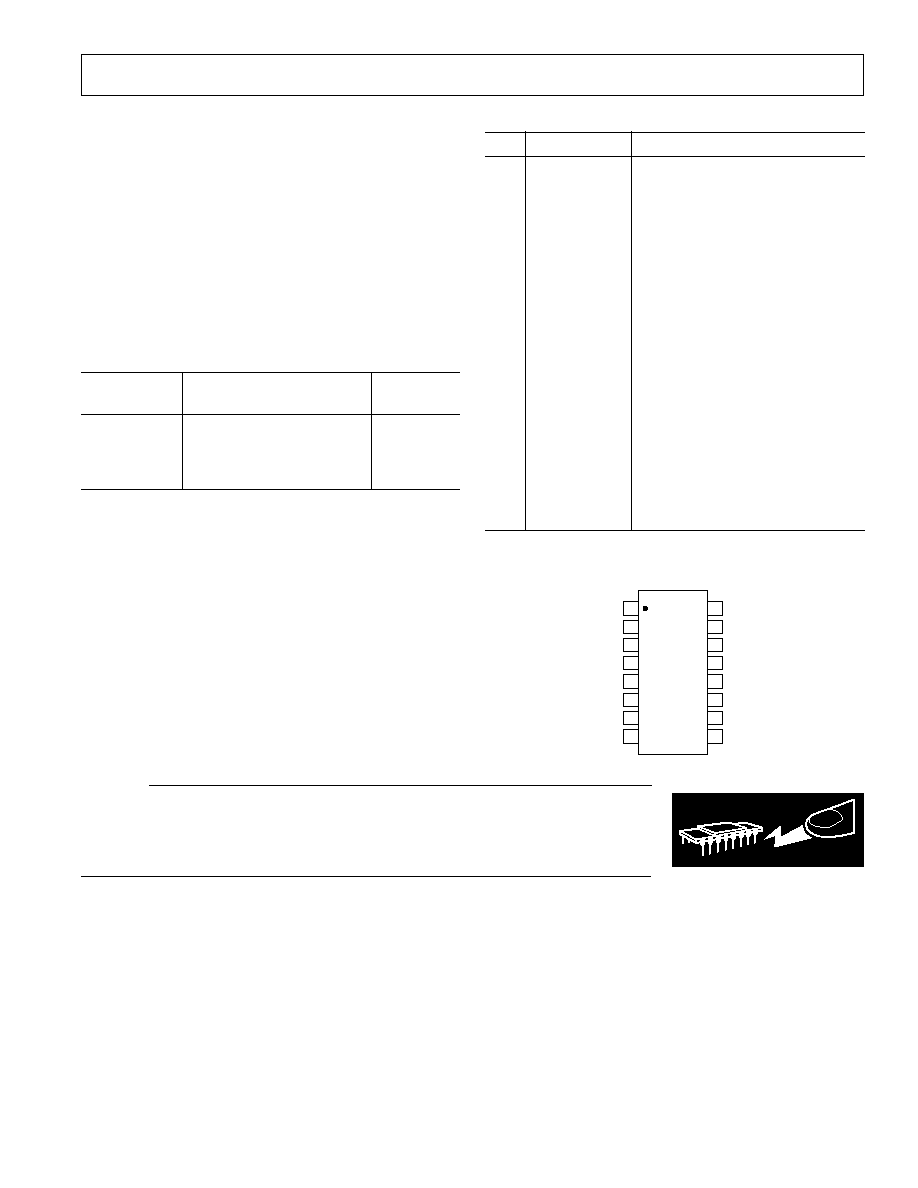
PIN DESCRIPTIONS
Pin
Mnemonic
Description
1
VPS1
Positive Supply Input
2
COM1
Common
3
LOHI
Local Oscillator Input Connection
4
COM2
Common
5
RFHI
RF Input, Noninverting
6
RFLO
RF Input, Inverting
7
MXOP
Mixer Output
8
VMID
Midpoint Supply Bias
Output
9
IFHI
IF Input, Noninverting
10
IFLO
IF Input, Inverting
11
RSSI
Received Signal Strength Indicator
Output
12
COM3
Output Common
13
FDBK
Offset-Null Feedback Loop Output
14
VPS2
Limiter Positive Supply Input
15
LMOP
Limiter Output
16
PRUP
Power-Up
TERMINAL DIAGRAM
WARNING!
ESD SENSITIVE DEVICE
CAUTION
ESD (electrostatic discharge) sensitive device. Electrostatic charges as high as 4000 V readily
accumulate on the human body and test equipment and can discharge without detection.
Although the AD608 features proprietary ESD protection circuitry, permanent damage may
occur on devices subjected to high energy electrostatic discharges. Therefore, proper ESD
precautions are recommended to avoid performance degradation or loss of functionality.
VPS1
COM1
PRUP
LMOP
RFHI
RFLO
MXOP
COM3
RSSI
IFLO
LOHI
COM2
VPS2
FDBK
VMID
IFHI
1
2
16
15
5
6
7
12
11
10
3
4
14
13
8
9
TOP VIEW
(Not to Scale)
AD608
REV. B
4
AD608
RF FREQUENCY MHz
CONVERSION GAIN dB
25.0
23.5
22.0
0
50
500
100 150 200 250 300 350 400 450
24.5
24.0
23.0
22.5
Figure 3. Mixer Conversion Gain vs.
Frequency
PRUP IN
VPOS
51.1
51.1
0.1µF
1nF
1nF
332
0.1µF
332
301
54.9
IF INPUT
0.1µF
10nF
RSSI OUTPUT
100
18nF
0.1µF
LMOP OUT
TRIGGER
4.7k
U1 74HC00
0.1µF
U1A
U1B
47k
1
2
3
4
5
6
7
8
16
15
14
13
12
11
10
9
AD608
VPS1
COM1
RFHI
RFLO
MXOP
LOHI
COM2
VMID
PRUP
LMOP
COM3
RSSI
IFLO
VPS2
FDBK
IFHI
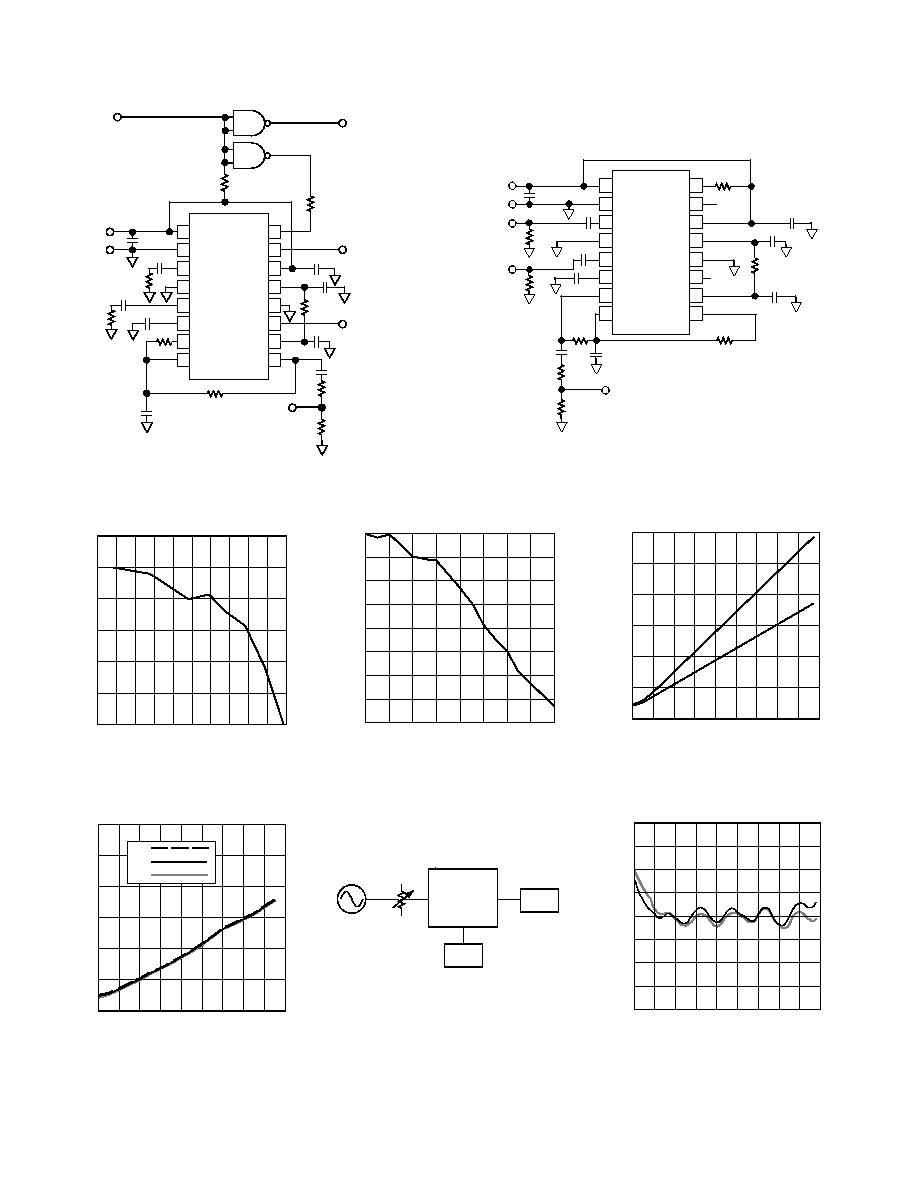
Figure 1. IF Test Board Schematic
INPUT POWER dBm
RSSI V
3.0
0
80 70
10
60 50 40
20 10
0
30
2.5
2.0
1.5
1.0
0.5
+85
+25
25
Figure 6. IF RSSI Output vs.
Temperature (3 V Supply)
IF FREQUENCY MHz
RESPONSE dB
0
8
0
10
80
20
30
40
50
60
70
1
4
5
6
7
2
3
Figure 4. Mixer IF Port Bandwidth
INPUT POWER AT IFHI dBm
RSSI V
3.0
0
80 70
10
60 50 40
20 10
0
30
2.5
2.0
1.5
1.0
0.5
5V
3V
Figure 5. IF RSSI Output vs. Supply
Voltage (Ambient Temperature)
IFHI
VPOS
RSSI
IF TEST BOARD
10.7 MHz
FLUKE 6082A
SYNTHESIZER
DCPS
3V
HP3366A
DMM
HP34401A
Figure 7. Test Circuit for IF RSSI Out-
put vs. Supply Voltage (Ambient Tem-
perature) (Figure 5) and IF RSSI
Output vs. Temperature (3 V Supply)
(Figure 6) and RSSI Error vs. Input
Power (Figure 8)
1
2
3
4
5
6
7
8
16
15
14
13
12
11
10
9
AD608
VPS1
COM1
RFHI
RFLO
MXOP
LOHI
COM2
VMID
PRUP
LMOP
COM3
RSSI
IFLO
VPS2
FDBK
IFHI
VPOS
LO IN
RF IN
IF OUT
NC
NC
0.1µF
1nF
51.1
1nF
332
301
0.1µF
54.9
51.1
1nF
0.1µF
332
10nF
100
18nF
18nF
47k
NC = NO CONNECT
Figure 2. Mixer Test Board Schematic
INPUT POWER dBm
RSSI ERROR dB
4.0
4.0
80 70
10
60 50 40
20 10
0
30
3.0
0
1.0
2.0
3.0
2.0
1.0
5V
3V
Figure 8. RSSI Error vs. Input Power
AD608
REV. B
5
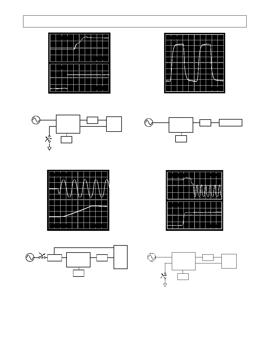
PRUP
RSSI
800mV/DIV
1V /DIV
100ns/DIV
100ns/DIV
Figure 9. RSSI Power-Up Response
IFHI
VPOS
RSSI
IF TEST BOARD
10.7 MHz
FLUKE 6082A
SYNTHESIZER
DCPS
3V
HP3366A
FET
PROBE
TEK P6201
PRUP
TRIGGER
CH 1
CH 2
HP54120A
DIGITAL
OSCILLOSCOPE
0dBm
Figure 10. Test Circuit for RSSI Power-Up Response
(Figure 9)
RSSI
800mV/DIV
IFHI
50ns/DIV
200mV/DIV
Figure 11. RSSI Pulse Response/RSSI Rise Time
IFHI
VPOS
RSSI
IF TEST BOARD
10.7 MHz
FLUKE 6082A
SYNTHESIZER
DCPS
3V
HP3366A
FET
PROBE
TEK P6201
CH 1
CH 2
HP54120A
DIGITAL
OSCILLOSCOPE
0dBm
COUPLER
MCL
ZDC-20-1
Figure 12. Test Circuit for RSSI Pulse Response/RSSI Rise
Time (Figure 11)
60mV/DIV
20ns/DIV
LMOP
Figure 13. Limiter Rise and Fall Times
IFHI
VPOS
LMOP
IF TEST BOARD
10.7 MHz
FLUKE 6082A
SYNTHESIZER
DCPS
3V
HP3366A
FET
PROBE
TEK P6201
HP54120A
0dBm
DIGITAL
OSCILLOSCOPE
Figure 14. Test Circuit for Limiter Rise and Fall Times
(Figure 13)
PRUP
100ns/DIV
1V/DIV
220mV/DIV
100ns/DIV
LMOP
Figure 15. Limiter Power-Up Response Time
IFHI
VPOS
LMOP
IF TEST BOARD
10.7 MHz
FLUKE 6082A
SYNTHESIZER
3V
HP6633A
FET
PROBE
TEK P6201
PRUP
TRIGGER
CH 1
CH 2
HP54120A
DIGITAL
OSCILLOSCOPE
0dBm
DCPS
Figure 16. Test Circuit for Limiter Power-Up Response
Time (Figure 15)
REV. B
6
AD608
INPUT POWER dBm
5
5
80 70
10
60 50 40
20 10
0
30
4
1
2
3
4
3
2
0
1
RELATIVE PHASE Degrees
Figure 17. Limiter Phase Performance vs.
Input Power at IFHI
IFHI
RSSI
IF TEST BOARD
10.7 MHz
FLUKE 6082A
SYNTHESIZER
DCPS
3V
HP3366A
FET
PROBE
TEK P6201
CH 1
TRIG
HP54120A
DIGITAL
OSCILLOSCOPE
MCL
ZDC-20-1
BPF
HP8447A
HP8494A
HP8495A
280kHz BW
10.7MHz CF
TOKO SK107MK1-A0-10
COUPLER
Figure 18. Test Circuit for Limiter Phase Performance vs.
Input Power at IFHI (Figure 17) and Limiter Jitter Perfor-
mance vs. Input Power at IFHI (Figure 19)
INPUT POWER AT IFHI dBm
10
0
80 70
10
60 50 40
20 10
0
30
9
4
3
2
1
8
7
5
6
RMS JITTER Degrees
Figure 19. Limiter Jitter Performance vs.
Input Power at IFHI
AD608
REV. B
7
THEORY OF OPERATION
The AD608 (Figure 20) consists of a mixer followed by a loga-
rithmic IF strip with RSSI and hard limited outputs. Each sec-
tion will be described below.
Mixer
The mixer is a doubly-balanced modified Gilbert cell mixer. Its
maximum input level for linear operation is
±
56.2 mV regard-
less of the impedance across the mixer's inputs, or 15 dBm for
a 50
input termination. The input impedance of the mixer
can be modeled as a simple parallel RC network; the values ver-
sus frequency are listed in Table I. The bandwidth from the RF
input to the IF output at MXOP pin is 1 dB at 30 MHz and
then falls off rapidly (Figure 4).
Mixer Gain
The mixer's conversion gain is the product of its transcon-
ductance and the impedance seen at pin MXOP. For a 330
parallel-terminated filter at 10.7 MHz, the load impedance is
165
, the gain is 24 dB, and the output is 15.85
×
56.2 mV, or
±
891 mV, centered on the midpoint of the supply voltage. For
other load impedances, the expression for the gain in dB is
G
dB
=
20 log
10
0.0961 R
L
(
)
The mixer's gain can be increased or decreased by changing R
L
,
the load impedance at pin MXOP. The limitations on the
mixer's gain are the
±
6 mA maximum output current at MXOP
and the maximum allowable voltage swing at pin MXOP, which
is
±
1.0 V for a 3 V supply or 5 V supply.
Table I. Mixer Input Impedance vs. Frequency
Frequency
Resistance
Capacitance
(MHz)
(Ohms)
(pF)
45
2800
3.1
70
2600
3.1
100
1800
3.1
200
1200
3.1
300
760
3.2
400
520
3.4
500
330
3.6
24dB MIXER GAIN
110dB LIMITER GAIN
90dB RSSI
BIAS
MXOP
MIXER
BPF
DRIVER
VMID
LO
PREAMP
AD608
RFHI
RFLO
IF INPUT
75dBm TO
+15dBm
2.
IFHI
IFLO
LMOP
VPS2
RSSI
FDBK
COM3
FINAL
LIMITER
100nF
10nF
330
±
50
µ
A
10.7MHz
BANDPASS
FILTER
330
MID-SUPPLY
IF BIAS
6
5
7
8
10
9
13
14
12
15
11
1
2
3
4
16
LIMITER
OUTPUT
400mVp-p
PRUP
RF INPUT
95 TO
15dBm
1.
VPS1 COM1
COM2
LOIP
RSSI OUTPUT
20mV/dB
0.2V TO 1.8V
3dB NOMINAL
INSERTION LOSS
+2.7V TO 5.5V
5-STAGE IF AMPLIFIER
(16dB PER STAGE)
7 FULL-WAVE
RECTIFIER CELLS
+2.7V TO 5.5V
LO INPUT
16dBm
CMOS LOGIC
INPUT
±
6mA MAX OUTPUT
(
±
890mV INTO 165
)
100
18nF
1. 15dBm =
±
56mV MAX FOR LINEAR OPERATION
2. 39.76mV RMS TO 396.6mV RMS FOR
±
1 dB
RSSI ACCURACY
NOTES:
Figure 20. Functional Block Diagram
REV. B
8
AD608
IF Filter Terminations
The AD608 was designed to drive a parallel-terminated 10.7 MHz
bandpass filter with a 330
impedance. With a 330
parallel-
terminated filter, pin MXOP sees a 165
termination and the
gain is nominally 24 dB. Other filter impedances and gains can
be accommodated by either accepting an increase or decrease in
gain in proportion to the filter impedance or by keeping the im-
pedance seen by MXOP a nominal 165
(by using resistive di-
viders or matching networks). Figure 21 shows a simple resistive
voltage divider for matching an assortment of filter impedances,
and Table II lists component values.
The Logarithmic IF Amplifier
The logarithmic IF amplifier consists of five amplifier stages
of 16 dB gain each, plus a final limiter. The IF bandwidth is
30 MHz (1 dB) and the limiting gain is 110 dB. The phase
skew is
±
3
°
from 75 dBm to +5 dBm (approximately 111
µ
V
p-p to 1.1 V p-p). The limiter output impedance is 200
and the limiter's output drive is
±
200 mV (400 mV p-p) into a
5 k
load. In the absence of an input signal, the limiter's output
will limit on noise fluctuations, which produces an output that
continues to swing 400 mV p-p but with random zero crossings.
Offset Feedback Loop
Because the logarithmic amplifier is dc coupled and has more
than 110 dB of gain from the input to the limiter output, a dc
offset at its input of even a few
µ
V would cause the output to
saturate. Thus, the AD608 uses a low frequency feedback loop
to null out the input offset. Referring to Figure 21, the loop
consists of a current source driven by the limiter, which sends
50
µ
A current pulses to pin FDBK. The pulses are low pass
filtered by a
-network consisting of C1, R4, and C5. The
smoothed dc voltage that results is subtracted from the input to
the IF amplifier at pin IFLO. Because this is a high gain ampli-
fier with a feedback loop, care should be taken in layout and
component values to prevent oscillation. Recommended values
for the common IFs of 450 kHz, 455 kHz, 6.5 MHz, and
10.7 MHz are listed in Table II.
24dB MIXER GAIN
110dB LIMITER GAIN
90dB RSSI
BIAS
MXOP
MIXER
BPF
DRIVER
VMID
LO
PREAMP
AD608
RFHI
RFLO
IFHI
IFLO
LMOP
VPS2
RSSI
FDBK
COM3
FINAL
LIMITER
100nF
C5
R1
±
50
µ
A
BANDPASS
FILTER
MID-SUPPLY
IF BIAS
6
5
7
8
10
9
13
14
12
15
11
1
2
3
4
16
PRUP
VPS1 COM1
COM2
LOHI
12dB NOMINAL
INSERTION LOSS
(ASSUMES 6dB IN FILTER)
5-STAGE IF AMPLIFIER
(16dB PER STAGE)
7 FULL-WAVE
RECTIFIER CELLS
R4
C1
+5V
C1
1
µ
F
LO INPUT
16dBm
C2
100pF
CMOS
LOGIC
INPUT
R2
R3
2MHz
LPF
47k
Figure 21. Applications Diagram for Common IFs and Filter Impedances
Table II. AD608 Filter Termination and Offset-Null Feedback Loop Resistor and Capacitor Values for Common IFs
Filter
Filter Termination Resistor
Offset Null
IF
Impedance
Values
1
for 24 dB of Mixer Gain
Feedback Loop Values
R1
R2
R3
R4
C1
C5
450 kHz
2
1500
174
1330
1500
1000
200 nF
100 nF
455 kHz
1500
174
1330
1500
1000
200 nF
100 nF
6.5 MHz
1000
178
825
1000
100
18 nF
10 nF
10.7 MHz
330
330
0
330
100
18 nF
10 nF
NOTES
1
Resistor values were calculated so that R1 + R2 = Z
FILTER
and R1 (R2+Z
FILTER
) = 165
.
2
Operation at IFs of 450 kHz and 455 kHz requires an external low pass filter with at least one pole at a cutoff frequency of 90 kHz (a decade below the ripple
at 900 kHz).

AD608
REV. B
9
RSSI Output
The logarithmic amplifier uses a successive detection architec-
ture. Each of the five stages has a full-wave detector; two addi-
tional high level detectors are driven through attenuators at the
input to the limiting amplifiers, for a total of seven detector
stages. Because each detector is a full-wave rectifier, the ripple
component in the resulting dc is at twice the IF. The AD608's
low-pass filter has a 2 MHz cutoff frequency, which is one
decade below the 21.4 MHz ripple that results from a 10.7 MHz
IF.
For operation at lower IFs such as 450 kHz or 455 kHz, the
AD608 requires an external low-pass filter with a single pole lo-
cated at 90 kHz, a decade below the 900 kHz ripple frequency
for these IFs. The RSSI range is from the noise level at approxi-
mately 80 dBm to overload at +15 dBm and is specified for
±
1 dB accuracy from 75 dBm to +5 dBm. The +15 dBm
maximum IF input is provided to accommodate bandpass filters
of lower insertion loss than the nominal 4 dB for 10.7 MHz
ceramic filters.
Digitizing the RSSI
In typical cellular radio applications, the RSSI output of the
AD608 will be digitized by an A/D converter. The AD608's
RSSI output is proportional to the power-supply voltage, which
not only allows the A/D converter to use the supply as a refer-
ence but also causes the RSSI output and the A/D converter's
output to track over power supply variations, reducing system
errors and component costs.
Power Consumption
The total power-supply current of the AD608 is a nominal
7.3 mA. The power is signal-dependent, partly as the RSSI
output increases (the current is increased by 200
µ
A at an RSSI
output of +1.8 V) but mostly due to the IF BPF consumption
when being driven to
±
891 mV assuming a 4 dB loss in this
filter and a peak input of +5 dBm to the log-IF amp, and tem-
perature dependent, as the biasing system used in the AD608 is
proportional to absolute temperature (PTAT).
Troubleshooting
The most common causes of problems with the AD608 are
incorrect component values for the offset feedback loop, poor
board layout, and pickup of RFI, which all cause the AD608 to
"lose" the low end (typically below 65 dBm) of its RSSI output
and cause the limiter to swing randomly. Both poor board lay-
out and incorrect component values in the offset feedback loop
can cause low level oscillations. Pickup of RFI can be caused by
improper layout and shielding of the circuit.
REV. B
10
AD608
Applications
Figure 22 shows the AD608 configured for operation in a digital
system at a 10.7 MHz IF. The filter's input and output imped-
ance are parallel terminated using 330
resistors and the con-
version gain is 24 dB. The RF port is terminated in 50
; in a
typical application the input would be matched to a SAW filter
using the impedance data shown previously in Table I.
Figure 23 shows the AD608 configured for narrowband FM op-
eration at a 450 kHz or 455 kHz with an external discriminator.
The IF filter has 1500
input and output impedances-- the
input is matched via a resistive divider and the output is termi-
nated in 1500
. The discriminator requires 1 V p-p drive from
a 1 k
source impedance, here provided by a gain-of-2.5 Class
A amplifier.
10.7MHz BPF Z = 330
R2
330
C5
0.1µF
R1
330
C2
100pF
C3
100pF
C4
100pF
C1
1µF
VPOS
LIMO
C6
10nF
SUPPLY
2.7V TO 5.5V
POWER-UP
3V CMOS
LIMITER
OUTPUT
VPOS 1V
±
200mV
RSSI OUTPUT
+0.2V TO +1.8V
(20mV/dB)
LO INPUT
16dBm
RF INPUT
95dBm
TO
15dBm
BIAS POINT
AT VPOS/2
IF BIAS POINT
DECOUPLING
BPF REVERSE
TERMINATION
OFFSET-CONTROL
LOOP FILTER
BPF
TERMINATION
C7
18nF
16
15
12
11
10
14
13
9
1
2
5
6
7
3
4
8
AD608
VPS1
COM1
RFHI
RFLO
MXOP
LOHI
COM2
VMID
PRUP
LMOP
COM3
RSSI
IFLO
VPS2
FDBK
IFHI
R3
100
R4
47k
R6
51.1
R5
51.1
Figure 22. Application at 10.7 MHz. The Bandpass Filter
Can Be a Toko Type SK107 or Murata Type SFE10.7
+5V
R1
51.1
C1 0.1µF
C2
1nF
GND
R2
51.1
1
2
3
4
5
6
7
8
16
15
14
13
12
11
10
9
AD608
VPS1
COM1
RFHI
RFLO
MXOP
LOHI
COM2
VMID
PRUP
LMOP
COM3
RSSI
IFLO
VPS2
FDBK
IFHI
R3
374
R4
1.5k
R6
1k
LOHI
RFHI
C3
1nF
R7
1130
F1
C7
0.1µF
C6 0.1µF
C8 0.1µF
C9
0.2µF
R5 200
C5 0.1µF
R14
8.66k
R15
24.9k
R13
402
R12
1k
CR1
CR2
R8
1k
R9
1k
C10
0.01µF
R11
3.3k
AUDIO
PRUP
RSSI
JUMPER
F1: TOKO HCFM2455B
F2: MURATA CFY455S
CR1, CR2: 1N60
Q1: 2N3906
F2
R10
3.3k
R16
47k
Q1
C11
0.1µF
C4
1nF
Figure 23. Narrowband FM Application at 450 kHz or 455 kHz
AD608
REV. B
11
PIN 1
0.1574 (4.00)
0.1497 (3.80)
0.2440 (6.20)
0.2284 (5.80)
1
16
9
8
0.0500 (1.27)
0.0160 (0.41)
8
°
0
°
0.0196 (0.50)
0.0099 (0.25)
x 45
°
0.0099 (0.25)
0.0075 (0.19)
0.0192 (0.49)
0.0138 (0.35)
0.0500
(1.27)
BSC
0.0688 (1.75)
0.0532 (1.35)
0.0098 (0.25)
0.0040 (0.10)
0.3937 (10.00)
0.3859 (9.80)
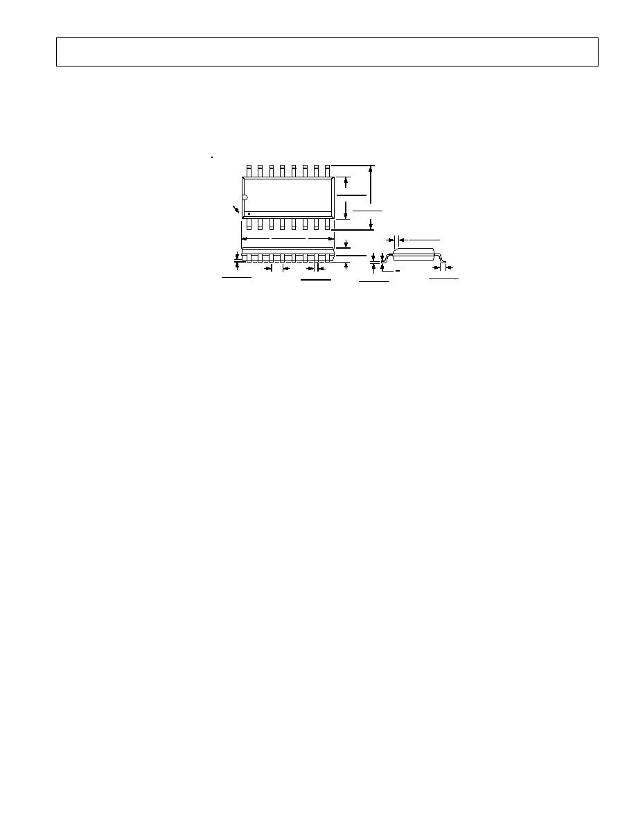
OUTLINE DIMENSIONS
Dimensions shown in inches and (mm).
16-Lead SOIC
(R-16A)

REV. B
12
AD608
PRINTED IN U.S.A.
C1990b27/96