/home/web/htmldatasheet/RUSSIAN/html/ad/210878
REV. D
Information furnished by Analog Devices is believed to be accurate and
reliable. However, no responsibility is assumed by Analog Devices for its
use, nor for any infringements of patents or other rights of third parties that
may result from its use. No license is granted by implication or otherwise
under any patent or patent rights of Analog Devices.
a
AD630
One Technology Way, P.O. Box 9106, Norwood, MA 02062-9106, U.S.A.
Tel: 781/329-4700
www.analog.com
Fax: 781/326-8703
© Analog Devices, Inc., 2001
Balanced Modulator/Demodulator
FUNCTIONAL BLOCK DIAGRAM
CM OFF
ADJ
CM OFF
ADJ
DIFF OFF
ADJ
DIFF OFF
ADJ
6
3
4
5
2.5k
AMP A
2.5k
AMP B
V
10k
10k
17
5k
8
9
10
COMP
19
18
1
15
7
16
14
13
11
12
R
IN
A
CHA+
CHA
R
IN
B
CHB+
CHB
SEL B
SEL A
2
20
COMP
+V
S
V
OUT
R
B
R
F
R
A
CHANNEL
STATUS
B/A
V
S
AD630
A
B
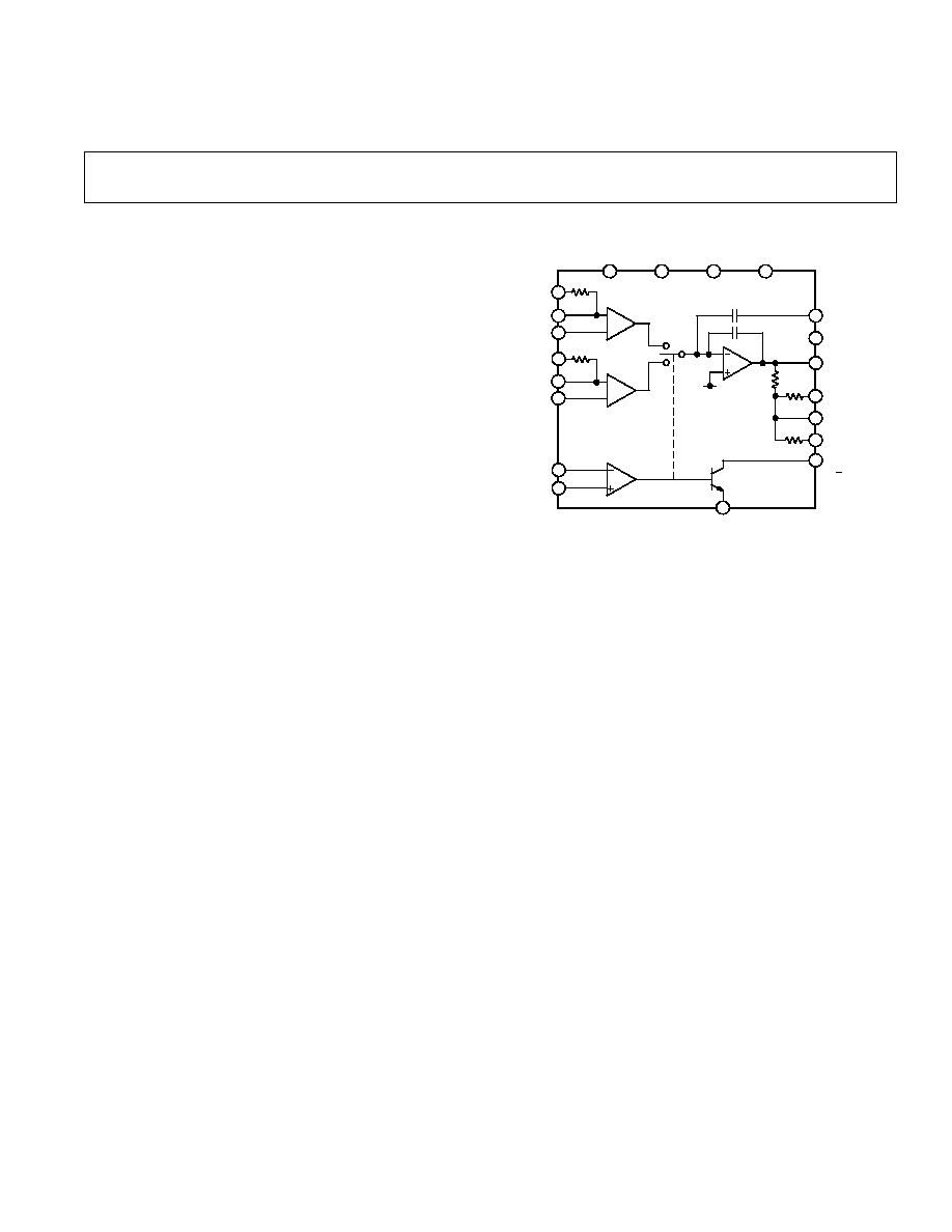
PRODUCT DESCRIPTION
The AD630 is a high precision balanced modulator which com-
bines a flexible commutating architecture with the accuracy and
temperature stability afforded by laser wafer trimmed thin-film
resistors. Its signal processing applications include balanced
modulation and demodulation, synchronous detection, phase
detection, quadrature detection, phase sensitive detection,
lock-in amplification and square wave multiplication. A network
of on-board applications resistors provides precision closed loop
gains of
± 1 and ± 2 with 0.05% accuracy (AD630B). These
resistors may also be used to accurately configure multiplexer
gains of +1, +2, +3 or +4. Alternatively, external feedback may
be employed allowing the designer to implement his own high
gain or complex switched feedback topologies.
The AD630 may be thought of as a precision op amp with two
independent differential input stages and a precision comparator
which is used to select the active front end. The rapid response
time of this comparator coupled with the high slew rate and fast
settling of the linear amplifiers minimize switching distortion. In
addition, the AD630 has extremely low crosstalk between chan-
nels of 100 dB @ 10 kHz.
The AD630 is intended for use in precision signal processing
and instrumentation applications requiring wide dynamic range.
When used as a synchronous demodulator in a lock-in amplifier
configuration, it can recover a small signal from 100 dB of inter-
fering noise (see lock-in amplifier application). Although optimized
for operation up to 1 kHz, the circuit is useful at frequencies up
to several hundred kilohertz.
Other features of the AD630 include pin programmable frequency
compensation, optional input bias current compensation resis-
tors, common-mode and differential-offset voltage adjustment,
and a channel status output which indicates which of the two
differential inputs is active. This device is now available to
Standard Military Drawing (DESC) numbers 5962-8980701RA
and 5962-89807012A.
PRODUCT HIGHLIGHTS
1. The configuration of the AD630 makes it ideal for signal
processing applications such as: balanced modulation and
demodulation, lock-in amplification, phase detection, and
square wave multiplication.
2. The application flexibility of the AD630 makes it the best
choice for many applications requiring precisely fixed gain,
switched gain, multiplexing, integrating-switching functions,
and high-speed precision amplification.
3. The 100 dB dynamic range of the AD630 exceeds that of any
hybrid or IC balanced modulator/demodulator and is compa-
rable to that of costly signal processing instruments.
4. The op-amp format of the AD630 ensures easy implementa-
tion of high gain or complex switched feedback functions.
The application resistors facilitate the implementation of
most common applications with no additional parts.
5. The AD630 can be used as a two channel multiplexer with
gains of +1, +2, +3, or +4. The channel separation of
100 dB @ 10 kHz approaches the limit which is achievable
with an empty IC package.
6. The AD630 has pin-strappable frequency compensation (no
external capacitor required) for stable operation at unity gain
without sacrificing dynamic performance at higher gains.
7. Laser trimming of comparator and amplifying channel offsets
eliminates the need for external nulling in most cases.
FEATURES
Recovers Signal from +100 dB Noise
2 MHz Channel Bandwidth
45 V/ s Slew Rate
120 dB Crosstalk @ 1 kHz
Pin Programmable Closed Loop Gains of 1 and 2
0.05% Closed Loop Gain Accuracy and Match
100 V Channel Offset Voltage (AD630BD)
350 kHz Full Power Bandwidth
Chips Available

REV. D
2
AD630SPECIFICATIONS
(@ 25 C and V
S
= 15 V unless otherwise noted.)
Model
AD630J/A
AD630K/B
AD630S
Min
Typ
Max
Min
Typ
Max
Min
Typ
Max
Unit
GAIN
Open Loop Gain
90
110
100
120
90
110
dB
±1, ±2 Closed Loop Gain Error
0.1
0.05
0.1
%
Closed Loop Gain Match
0.1
0.05
0.1
%
Closed Loop Gain Drift
2
2
2
ppm/
°C
CHANNEL INPUTS
V
IN
Operational Limit
1
(V
S
+ 4 V) to (+V
S
1 V)
(V
S
+ 4 V) to (+V
S
1 V)
(V
S
+ 4 V) to (+V
S
1 V)
Volts
Input Offset Voltage
500
100
500
µV
Input Offset Voltage
T
MIN
to T
MAX
800
160
1000
µV
Input Bias Current
100
300
100
300
100
300
nA
Input Offset Current
10
50
10
50
10
50
nA
Channel Separation @ 10 kHz
100
100
100
dB
COMPARATOR
V
IN
Operational Limit
1
(V
S
+ 3 V) to (+V
S
1.5 V)
(V
S
+ 3 V) to (+V
S
1.5 V)
(V
S
+ 3 V) to (+V
S
1.3 V)
Volts
Switching Window
±1.5
±1.5
±1.5
mV
Switching Window
T
MIN
to T
MAX
±2.0
±2.0
±2.5
mV
Input Bias Current
100
300
100
300
100
300
nA
Response Time (5 mV to +5 mV Step)
200
200
200
ns
Channel Status
I
SINK
@ V
OL
= V
S
+ 0.4 V
2
1.6
1.6
1.6
mA
Pull-Up Voltage
(V
S
+ 33 V)
(V
S
+ 33 V)
(V
S
+ 33 V)
Volts
DYNAMIC PERFORMANCE
Unity Gain Bandwidth
2
2
2
MHz
Slew Rate
3
45
45
45
V/
µs
Settling Time to 0.1% (20 V Step)
3
3
3
µs
OPERATING CHARACTERISTICS
Common-Mode Rejection
85
105
90
110
90
110
dB
Power Supply Rejection
90
110
90
110
90
110
dB
Supply Voltage Range
±5
±16.5
±5
±16.5
±5
±16.5
Volts
Supply Current
4
5
4
5
4
5
mA
OUTPUT VOLTAGE, @ R
L
= 2 k
T
MIN
to T
MAX
±10
±10
±10
Volts
Output Short Circuit Current
25
25
25
mA
TEMPERATURE RANGES
Rated PerformanceN Package
0
70
0
70
N/A
°C
Rated Performance
D Package
25
+85
25
+85
55
+125
°C
NOTES
1
If one terminal of each differential channel or comparator input is kept within these limits the other terminal may be taken to the positive supply.
2
I
SINK
@ V
OL
= (V
S
+ 1) volt is typically 4 mA.
3
Pin 12 Open. Slew rate with Pins 12 and 13 shorted is typically 35 V/
µs.
Specifications subject to change without notice.
REV. D
AD630
3
ABSOLUTE MAXIMUM RATINGS
Supply Voltage . . . . . . . . . . . . . . . . . . . . . . . . . . . . . . . .
±18 V
Internal Power Dissipation . . . . . . . . . . . . . . . . . . . . 600 mW
Output Short Circuit to Ground . . . . . . . . . . . . . . . Indefinite
Storage Temperature, Ceramic Package . . . 65
°C to +150°C
Storage Temperature, Plastic Package . . . . . 55
°C to +125°C
Lead Temperature Range (Soldering, 10 sec) . . . . . . . . 300
°C
Max Junction Temperature . . . . . . . . . . . . . . . . . . . . . . 150
°C
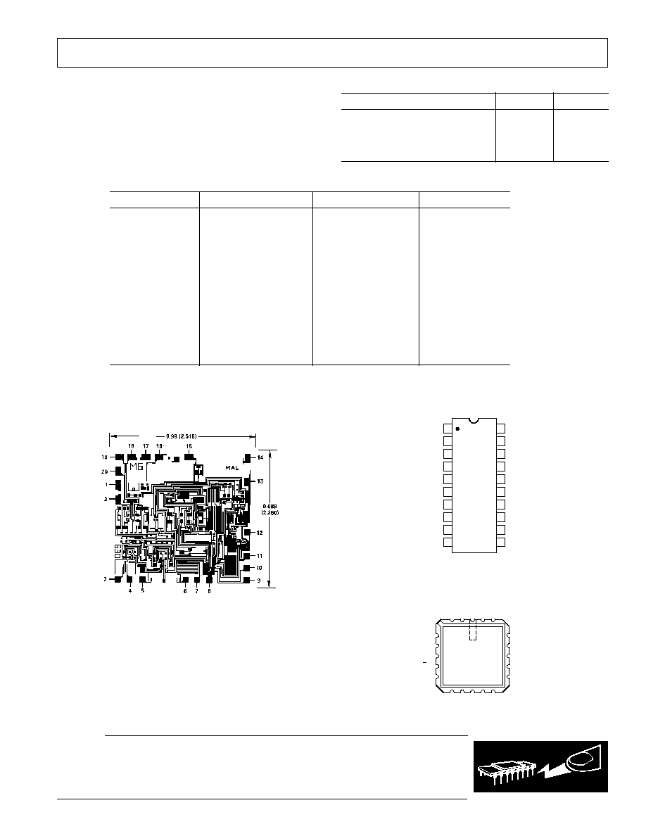
PIN CONFIGURATIONS
20-Lead DIP (D-20 and N-20), 20-Lead SOIC (R-20)
14
13
12
11
17
16
15
20
19
18
10
9
8
1
2
3
4
7
6
5
TOP VIEW
(Not to Scale)
AD630
R
IN
A
R
IN
B
CH B+
CH B
CH A
CH A+
DIFF OFF ADJ
DIFF OFF ADJ
R
B
R
F
R
A
CM OFF ADJ
CM OFF ADJ
V
S
SEL B
SEL A
+V
S
COMP
V
OUT
CHANNEL STATUS B/
A
20-Contact LCC (E-20A)
20 19
1
2
3
18
14
15
16
17
4
5
6
7
8
9 10 11 12 13
TOP VIEW
(Not to Scale)
AD630
DIFF OFF ADJ
CM OFF ADJ
CM OFF ADJ
CHANNEL STATUS B/A
V
S
CH B+
R
IN
B
R
A
R
F
R
B
DIFF
OFF ADJ
CH A+
R
IN
A
CH A
CH B
SEL B
SEL A
+V
S
COMP
V
OUT
ORDERING GUIDE
Model
Temperature Ranges
Package Description
Package Option
AD630JN
0
°C to 70°C
Plastic DIP
N-20
AD630KN
0
°C to 70°C
Plastic DIP
N-20
AD630AR
25
°C to +85°C
SOIC
R-20
AD630AR-REEL
25
°C to +85°C
13" Tape and Reel
R-20
AD630AD
25
°C to +85°C
Side Brazed DIP
D-20
AD630BD
25
°C to +85°C
Side Brazed DIP
D-20
AD630SD
55
°C to +125°C
Side Brazed DIP
D-20
AD630SD/883B
55
°C to +125°C
Side Brazed DIP
D-20
5962-8980701RA
55
°C to +125°C
Side Brazed DIP
D-20
AD630SE/883B
55
°C to +125°C
LCC
E-20A
5962-89807012A
55
°C to +125°C
LCC
E-20A
AD630JCHIPS
0
°C to 70°C
Chip
AD630SCHIPS
55
°C to +125°C
Chip
THERMAL CHARACTERISTICS
JC
JA
20-Lead Plastic DIP (N)
24
°C/W
61
°C/W
20-Lead Ceramic DIP (D)
35
°C/W
120
°C/W
20-Lead Leadless Chip Carrier (E)
35
°C/W
120
°C/W
20-Lead SOIC (R-20)
38
°C/W
75
°C/W
CHIP METALIZATION AND PINOUT
Dimensions shown in inches and (mm).
Contact factory for latest dimensions.
CHIP AVAILABILITY
The AD630 is available in laser trimmed, passivated chip
form. The figure shows the AD630 metalization pattern, bond-
ing pads and dimensions. AD630 chips are available; consult
factory for details.
CAUTION
ESD (electrostatic discharge) sensitive device. Electrostatic charges as high as 4000 V readily
accumulate on the human body and test equipment and can discharge without detection. Although
the AD630 features proprietary ESD protection circuitry, permanent damage may occur on devices
subjected to high-energy electrostatic discharges. Therefore, proper ESD precautions are
recommended to avoid performance degradation or loss of functionality.
WARNING!
ESD SENSITIVE DEVICE
REV. D
AD630
4
REV. D
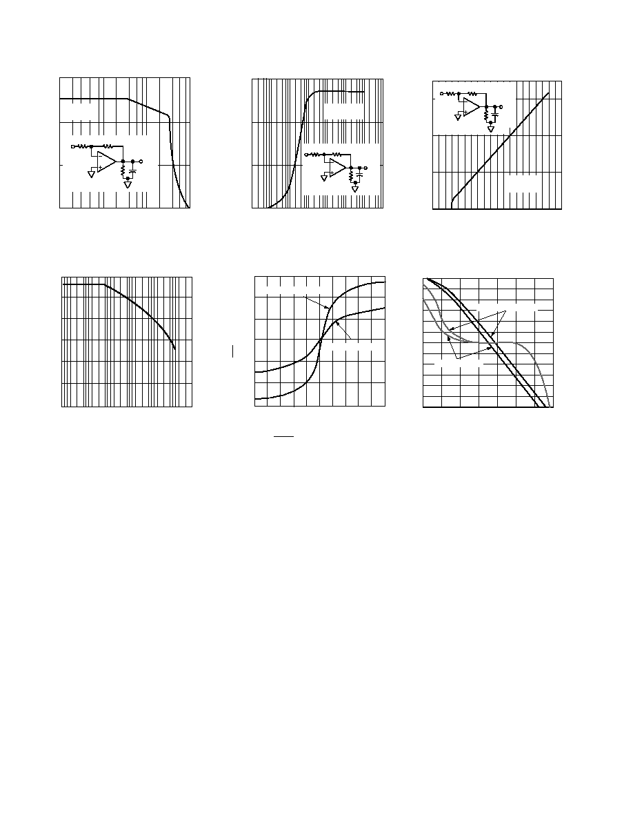
10
15
5
1
10
100
1k
10k
100k
1M
RESISTIVE LOAD
C
L
= 100pF
f = 1kHz
CAP IN
5k
V
O
100pF
R
L
V
i
5k
OUTPUT VOLTAGE
V
TPC 2. Output Voltage vs. Resistive
Load
INPUT VOLTAGE V
DV
O
dt
V/
s
60
0
60
5
3
4
2
1
1
40
20
40
20
4
0
2
3
5
UNCOMPENSATED
COMPENSATED
TPC 5.
dV
dt
O
vs. Input Voltage
10
18
5
0
5
10
15
SUPPLY VOLTAGE V
OUTPUT VOLTAGE
V
15
5k
100pF
V
i
5k
2k
V
O
f = 1kHz
C
L
= 100pF
TPC 3. Output Voltage Swing vs.
Supply Voltage
FREQUENCY Hz
120
60
0
1M
100
100
80
20
40
10
1k
100k
10k
UNCOMPENSATED
10M
0
45
90
OPEN LOOP GAIN
dB
135
180
COMPENSATED
OPEN LOOP PHASE
Degrees
TPC 6. Gain and Phase vs. Frequency
FREQUENCY Hz
15
10
5
1k
10k
1M
100k
R
L
=
2k
C
L
= 100pF
2k
5k
5k
V
i
V
O
100pF
OUTPUT VOLTAGE
V
TPC 1. Output Voltage vs. Frequency
FREQUENCY Hz
COMMON MODE REJECTION
dB
120
60
0
1
10
100k
100
1k
10k
100
80
40
20
TPC 4. Common-Mode Rejection
vs. Frequency
AD630Typical Performance Characteristics
4
REV. D
AD630
5
20mV
500ns
20mV
100
90
10
0%
20mV/DIV
(V
o
)
20mV/DIV
(V
i
)
TOP TRACE: Vo
BOTTOM TRACE: Vi
5k
10k
10k
V
i
CH
A
CH
B
12
V
O
2
20
19
18
13
9
10
14
16
15
TPC 7. Channel-to-Channel Switch-Settling Characteristic
100
90
10
0%
100mV
500ns
50mV
1mV
50mV/DIV
(V
i
)
1mV/DIV
(A)
TOP TRACE: Vi
MIDDLE TRACE: SETTLING
ERROR (A)
BOTTOM TRACE: Vo
100mV/DIV
(V
o
)
12
CH A
MIDDLE
TRACE
(A)
10k
10k
V
O
BOTTOM
TRACE
TEKTRONIX
7A13
10k
1k
30pF
10k
V
i
TOP
TRACE
2
20
13
14
15
TPC 8. Small Signal Noninverting Step Response
100
90
10
0%
10V
10V
1mV
TOP TRACE: Vi
MIDDLE TRACE: SETTLING
ERROR (B)
BOTTOM TRACE: Vo
5 s
10V 20kHz
(V
i
)
1mV/DIV
(B)
10V/DIV
(V
o
)
12
CH A
10k
10k
V
O
BOTTOM
TRACE
10k
V
i
TOP
TRACE
(B)
MIDDLE
TRACE
10k
HP5082-2811
20
2
13
14
15
TPC 9. Large Signal Inverting Step Response
REV. D
AD630
6
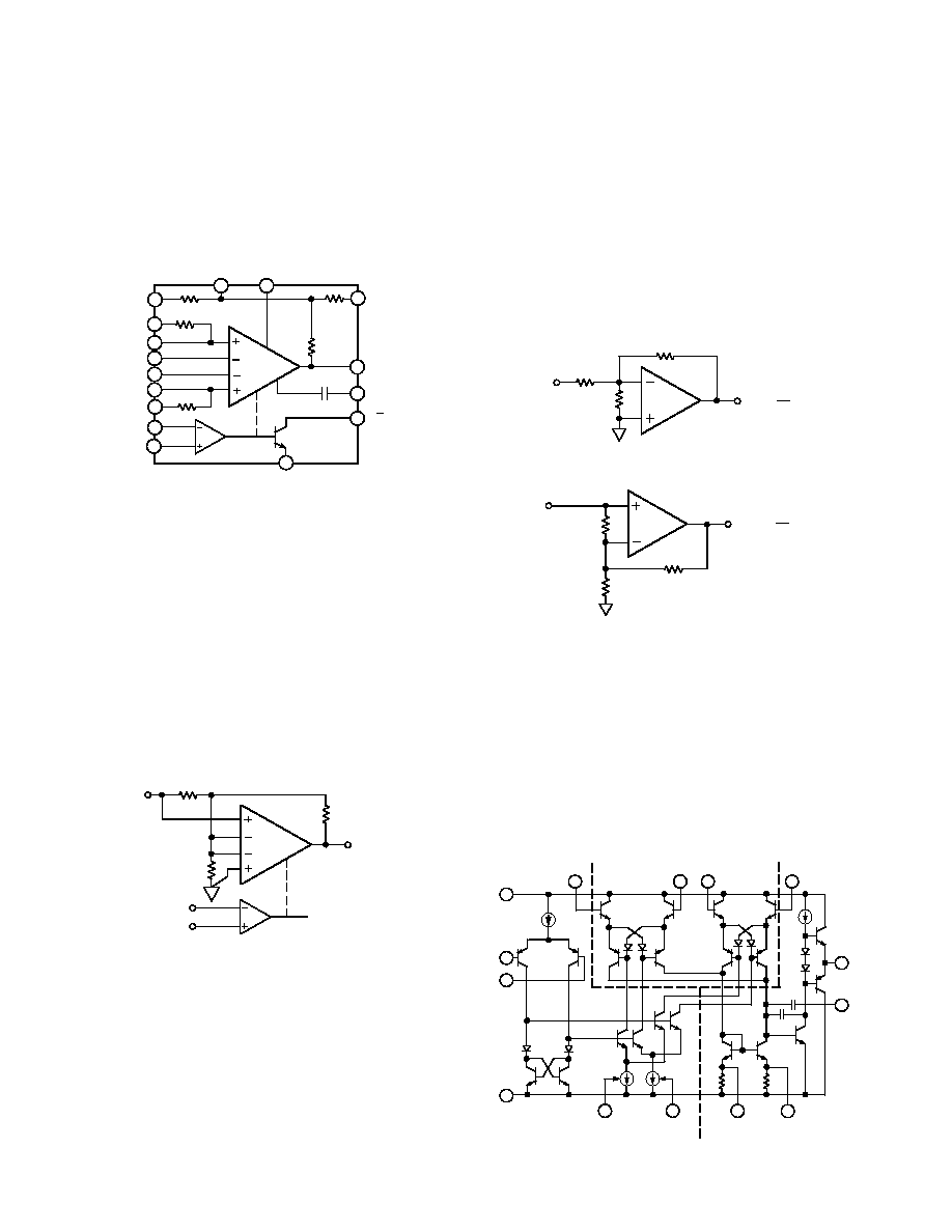
TWO WAYS TO LOOK AT THE AD630
The functional block diagram of the AD630 (see page 1) also
shows the pin connections of the internal functions. An alternative
architectural diagram is shown in Figure 1. In this diagram, the
individual A and B channel preamps, the switch, and the inte-
grator output amplifier are combined in a single op amp. This
amplifier has two differential input channels, only one of which
is active at a time.
11
15
2
20
19
18
17
8
7
12
14
13
9
10
R
A
5k
2.5k
R
F
10k
1
16
2.5k
+V
S
R
B
10k
SEL B
SEL A
B/A
A
B
V
S
Figure 1. Architectural Block Diagram
HOW THE AD630 WORKS
The basic mode of operation of the AD630 may be more easy to
recognize as two fixed gain stages which may be inserted into the
signal path under the control of a sensitive voltage comparator.
When the circuit is switched between inverting and noninverting
gain, it provides the basic modulation/demodulation function. The
AD630 is unique in that it includes Laser-Wafer-Trimmed thin-
film feedback resistors on the monolithic chip. The configuration
shown in Figure 2 yields a gain of
±2 and can be easily changed to
±1 by shifting R
B
from its ground connection to the output.
The comparator selects one of the two input stages to complete
an operational feedback connection around the AD630. The
deselected input is off and has negligible effect on the operation.
A
B
R
A
5k
R
F
10k
V
O
R
B
10k
V
i
2
20
19
18
13
15
16
14
9
10
Figure 2. AD630 Symmetric Gain (
±2)
When channel B is selected, the resistors R
A
and R
F
are con-
nected for inverting feedback as shown in the inverting gain
configuration diagram in Figure 3. The amplifier has sufficient
loop gain to minimize the loading effect of R
B
at the virtual
ground produced by the feedback connection. When the sign of
the comparator input is reversed, input B will be deselected and
A will be selected. The new equivalent circuit will be the nonin-
verting gain configuration shown below. In this case R
A
will appear
across the op amp input terminals, but since the amplifier drives
this difference voltage to zero, the closed loop gain is unaffected.
The two closed loop gain magnitudes will be equal when R
F
/R
A
= 1 + R
F
/R
B
, which will result from making R
A
equal to R
F
R
B
/
(R
F
+ R
B
) the parallel equivalent resistance of R
F
and R
B
.
The 5 k
and the two 10 k resistors on the AD630 chip can
be used to make a gain of two as shown here. By paralleling
the 10 k
resistors to make R
F
equal 5 k
and omitting R
B
the circuit can be programmed for a gain of
± 1 (as shown in
Figure 9a). These and other configurations using the on-chip
resistors present the inverting inputs with a 2.5 k
source imped-
ance. The more complete AD630 diagrams show 2.5 k
resistors
available at the noninverting inputs which can be conveniently
used to minimize errors resulting from input bias currents.
R
A
5k
R
F
10k
R
B
10k
V
i
V
O
=
R
F
R
A
V
i
Figure 3. Inverting Gain Configuration
R
A
5k
R
F
10k
R
B
10k
V
i
V
O
=
(
1+
R
F
R
B
)
V
i
Figure 4. Noninverting Gain Configuration
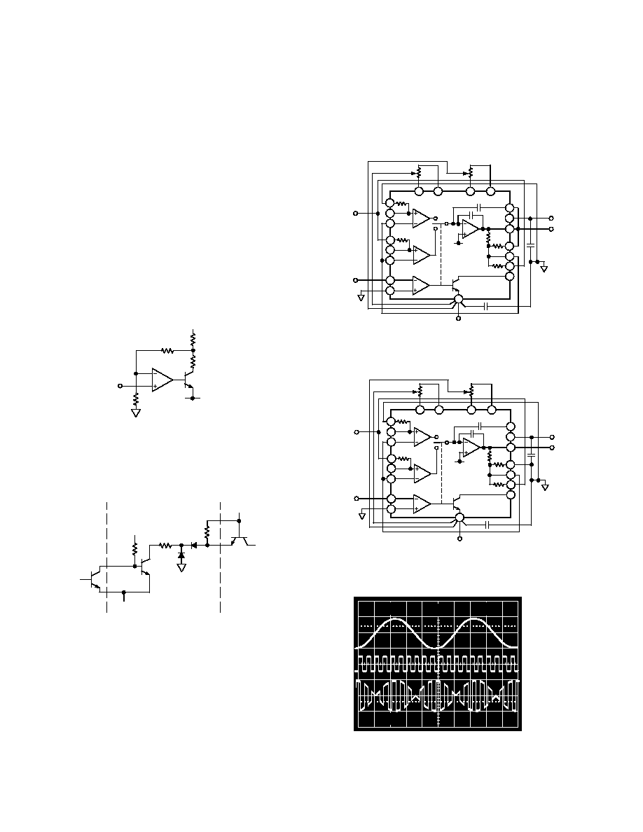
CIRCUIT DESCRIPTION
The simplified schematic of the AD630 is shown in Figure 5.
It has been subdivided into three major sections, the comparator,
the two input stages and the output integrator. The compara-
tor consists of a front end made up of Q52 and Q53, a flip-flop
load formed by Q3 and Q4, and two current steering switching
cells Q28, Q29 and Q30, Q31. This structure is designed so that
a differential input voltage greater than 1.5 mV in magnitude
applied to the comparator inputs will completely select one the
switching cells. The sign of this input voltage determine which
of the two switching cells is selected.
20
11
3
4
5
6
19
2
18
13
12
SEL A
SEL B
DIFF
OFF ADJ
DIFF
OFF ADJ
CM
OFF ADJ
CM
OFF ADJ
COMP
Q74
Q44
CH B
CH B+
CH A+
CH A
i55
Q4
Q3
Q28
Q31
Q30
Q32
C122
C121
i22
i23
V
S
V
O
i73
Q52
Q53
+V
S
Q65
Q34
Q33
Q62
Q35
Q36
Q67
Q70
Q25
Q24
Q29
10
9
8
Figure 5. AD630 Simplified Schematic
REV. D
AD630
7
The collectors of each switching cell connect to an input trans-
conductance stage. The selected cell conveys bias currents i
22
and i
23
to the input stage it controls, causing it to become active.
The deselected cell blocks the bias to its input stage which, as a
consequence, remains off.
The structure of the transconductance stages is such that they
present a high impedance at their input terminals and draw no
bias current when deselected. The deselected input does not
interfere with the operation of the selected input insuring maxi-
mum channel separation.
Another feature of the input structure is that it enhances the
slew rate of the circuit. The current output of the active
stage follows a quasi-hyperbolic-sine relationship to the dif-
ferential input voltage. This means that the greater the input
voltage, the harder this stage will drive the output integrator,
and hence, the faster the output signal will move. This feature
helps insure rapid, symmetric settling when switching between
inverting and noninverting closed loop configurations.
The output section of the AD630 includes a current mirror-
load (Q24 and Q25), an integrator-voltage gain stage (Q32),
and complementary output buffer (Q44 and Q74). The outputs of
both transconductance stages are connected in parallel to the
current mirror. Since the deselected input stage produces no
output current and presents a high impedance at its outputs,
there is no conflict. The current mirror translates the differen-
tial output current from the active input transconductance
amplifier into single ended form for the output integrator. The
complementary output driver then buffers the integrator output
produce a low impedance output.
OTHER GAIN CONFIGURATIONS
Many applications require switched gains other than the
±1 and
±2 which the self-contained applications resistors provide. The
AD630 can be readily programmed with three external resistors
over a wide range of positive and negative gain by selecting and
R
B
and R
F
to give the noninverting gain 1 + R
F
/R
B
and subsequent
R
A
to give the desired inverting gain. Note that when the inverting
magnitude equals the noninverting magnitude, the value of R
A
is
found to be R
B
R
F
/(R
B
+ R
F
). That is, R
A
should equal the parallel
combination of R
B
and R
F
to match positive and negative gain.
The feedback synthesis of the AD630 may also include reactive
impedance. The gain magnitudes will match at all frequencies if
the A impedance is made to equal the parallel combination of
the B and F impedances. Essentially the same considerations
apply to the AD630 as to conventional op-amp feedback circuits.
Virtually any function which can be realized with simple nonin-
verting "L network" feedback can be used with the AD630.
A common arrangement is shown in Figure 6. The low fre-
quency gain of this circuit is 10. The response will have a pole
(3 dB) at a frequency f 1/(2
100 kC) and a zero (3 dB
from the high frequency asymptote) at about 10 times this
frequency. The 2 k
resistor in series with each capacitor mitigates
the loading effect on circuitry driving this circuit, eliminates stabil-
ity problems, and has a minor effect on the pole-zero locations.
As a result of the reactive feedback, the high frequency com-
ponents of the switched input signal will be transmitted at
unity gain while the low frequency components will be ampli-
fied. This arrangement is useful in demodulators and lock-in
amplifiers. It increases the circuit dynamic range when the
modulation or interference is substantially larger than the
desired signal amplitude. The output signal will contain the
desired signal multiplied by the low frequency gain (which may
be several hundred for large feedback ratios) with the switching
signal and interference superimposed at unity gain.
C
V
S
A
B
10k
V
O
11.11k
12
V
i
100k
2k
C
2k
2
20
19
18
13
7
8
9
10
Figure 6. AD630 with External Feedback
SWITCHED INPUT IMPEDANCE
The noninverting mode of operation is a high input impedance
configuration while the inverting mode is a low input impedance
configuration. This means that the input impedance of the
circuit undergoes an abrupt change as the gain is switched
under control of the comparator. If gain is switched when the
input signal is not zero, as it is in many practical cases, a tran-
sient will be delivered to the circuitry driving the AD630. In
most applications, this will require the AD630 circuit to be
driven by a low impedance source which remains "stiff " at high
frequencies. Generally this will be a wideband buffer amplifier.
FREQUENCY COMPENSATION
The AD630 combines the convenience of internal frequency
compensation with the flexibility of external compensation by
means of an optional self-contained compensation capacitor.
In gain of
±2 applications the noise gain which must be addressed
for stability purposes is actually 4. In this circumstance, the
phase margin of the loop will be on the order of 60
° without the
optional compensation. This condition provides the maximum
bandwidth and slew-rate for closed-loop gains of |2| and above.
When the AD630 is used as a multiplexer, or in other configura-
tions where one or both inputs are connected for unity gain
feedback, the phase margin will be reduced to less than 20
°.
This may be acceptable in applications where fast slewing is a
first priority, but the transient response will not be optimum.
For these applications, the self-contained compensation capacitor
may be added by connecting Pin 12 to Pin 13. This connection
reduces the closed loop bandwidth somewhat, and improves the
phase margin.
For intermediate conditions, such as gain of
± 1 where loop
attenuation is 2, use of the compensation should be determined
by whether bandwidth or settling response must be optimized.
The optional compensation should also be used when the AD630
is driving capacitive loads or whenever conservative frequency
compensation is desired.
OFFSET VOLTAGE NULLING
The offset voltages of both input stages and the comparator
have been pretrimmed so that external trimming will only be
required in the most demanding applications. The offset adjust-
ment of the two input channels is accomplished by means of a
differential and common-mode scheme. This facilitates fine
adjustment of system errors in switched gain applications. With
REV. D
AD630
8
system input tied to 0 V, and a switching or carrier waveform
applied to the comparator, a low level square wave will appear at
the output. The differential offset adjustment pot can be used to
null the amplitude of this square wave (Pins 3 and 4). The
common-mode offset adjustment can be used to zero the residual
dc output voltage (Pins 5 and 6). These functions should be
implemented using 10k trim pots with wipers connected directly
to Pin 8 as shown in Figures 9a and 9b.
CHANNEL STATUS OUTPUT
The channel status output, Pin 7, is an open collector output
referenced to V
S
which can be used to indicate which of the
two input channels is active. The output will be active (pulled
low) when Channel A is selected. This output can also be used
to supply positive feedback around the comparator. This produces
hysteresis which serves to increase noise immunity. Figure 7
shows an example of how hysteresis may be implemented. Note
that the feedback signal is applied to the inverting () terminal
of the comparator to achieve positive feedback. This is because
the open collector channel status output inverts the output sense
of the internal comparator.
1M
100k
100k
15V
+5V
100
7
8
9
10
Figure 7. Comparator Hysteresis
The channel status output may be interfaced with TTL inputs
as shown in Figure 8. This circuit provides appropriate level
shifting from the open-collector AD630 channel status output to
TTL inputs.
15V
+5V
TTL INPUT
AD630
+15V
IN 914's
6.8k
22k
100k
2N2222
7
8
Figure 8. Channel Status--TTL Interface
APPLICATIONS: BALANCED MODULATOR
Perhaps the most commonly used configuration of the AD630 is
the balanced modulator. The application resistors provide precise
symmetric gains of
±1 and ±2. The ±1 arrangement is shown in
Figure 9a and the
±2 arrangement is shown in Figure 9b. These
cases differ only in the connection of the 10 k
feedback resistor
(Pin 14) and the compensation capacitor (Pin 12). Note the use
of the 2.5 k
bias current compensation resistors in these
examples. These resistors perform the identical function in the
±1 gain case. Figure 10 demonstrates the performance of the
AD630 when used to modulate a 100 kHz square wave carrier
with a 10 kHz sinusoid. The result is the double sideband sup-
pressed carrier waveform.
These balanced modulator topologies accept two inputs, a signal
(or modulation) input applied to the amplifying channels, and a
reference (or carrier) input applied to the comparator.
MODULATED
OUTPUT
SIGNAL
CARRIER
INPUT
CM
ADJ
DIFF
ADJ
2.5k
AMP A
AMP B
V
10k
10k
5k
9
10
COMP
1
15
7
16
14
13
12
2
20
+V
S
V
S
AD630
A
B
2.5k
19
18
17
11
8
6
5
10k
4
3
10k
MODULATION
INPUT
Figure 9a. AD630 Configured as a Gain-of-One Balanced
Modulator
MODULATED
OUTPUT
SIGNAL
CARRIER
INPUT
CM
ADJ
DIFF
ADJ
2.5k
AMP A
AMP B
V
10k
10k
5k
9
10
COMP
1
15
7
16
14
13
12
2
20
+V
S
V
S
AD630
A
B
2.5k
19
18
17
11
8
6
5
10k
4
3
10k
MODULATION
INPUT
Figure 9b. AD630 Configured as a Gain-of-Two Balanced
Modulator
10V
5V
5V
20 s
MODULATION
INPUT
CARRIER
INPUT
OUTPUT
SIGNAL
Figure 10. Gain-of-Two Balanced Modulator Sample
Waveforms
REV. D
AD630
9
BALANCED DEMODULATOR
The balanced modulator topology described above will also act as
a balanced demodulator if a double sideband suppressed carrier
waveform is applied to the signal input and the carrier signal is
applied to the reference input. The output under these circumstances
will be the baseband modulation signal. Higher order carrier
components will also be present which can be removed with a
low-pass filter. Other names for this function are synchronous
demodulation and phase-sensitive detection.
PRECISION PHASE COMPARATOR
The balanced modulator topologies of Figures 9a and 9b can
also be used as precision phase comparators. In this case, an ac
waveform of a particular frequency is applied to the signal input
and a waveform of the same frequency is applied to the refer-
ence input. The dc level of the output (obtained by low-pass
filtering) will be proportional to the signal amplitude and phase
difference between the input signals. If the signal amplitude is
held constant, then the output can be used as a direct indication
of the phase. When these input signals are 90
° out of phase, they
are said to be in quadrature and the AD630 dc output will be zero.
PRECISION RECTIFIER-ABSOLUTE VALUE
If the input signal is used as its own reference in the balanced
modulator topologies, the AD630 will act as a precision recti-
fier. The high-frequency performance will be superior to that
which can be achieved with diode feedback and op amps. There
are no diode drops which the op amp must "leap over" with the
commutating amplifier.
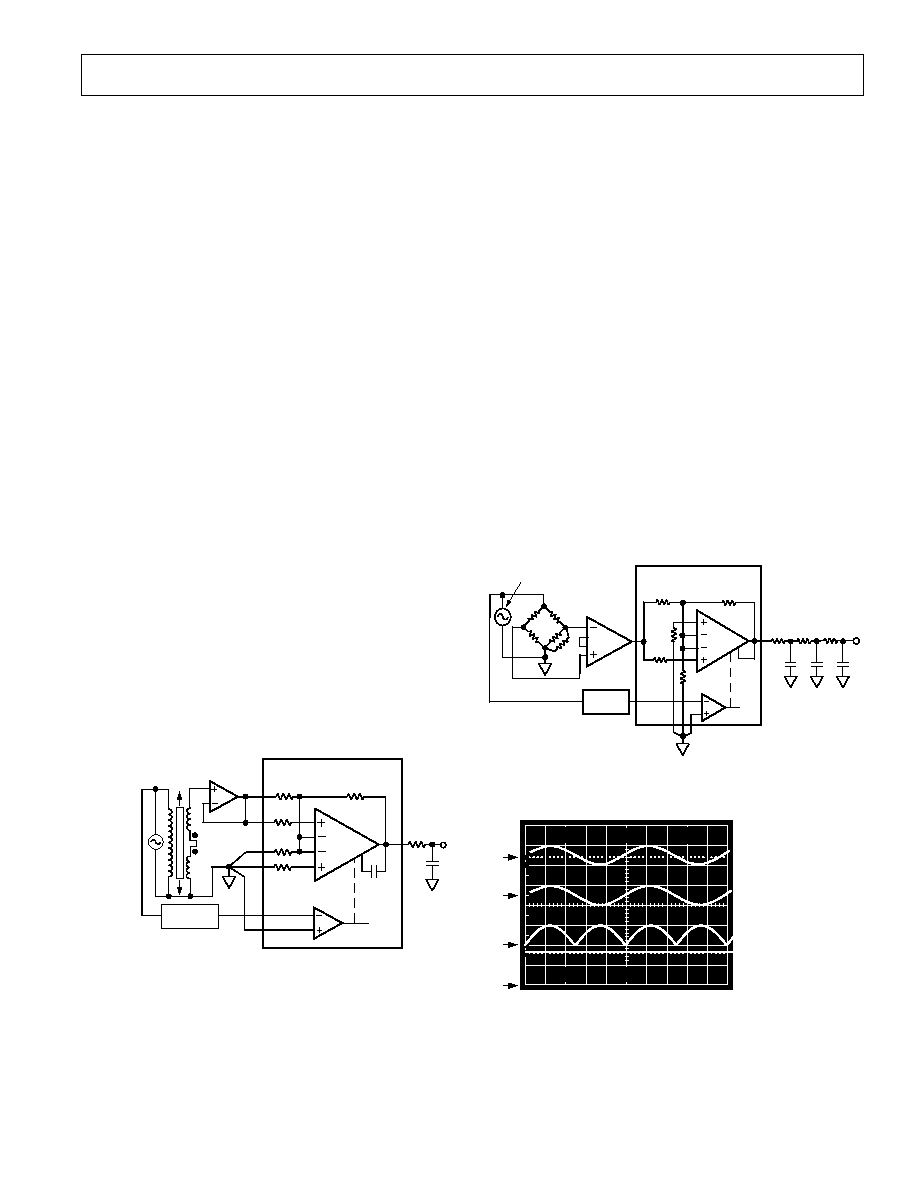
LVDT SIGNAL CONDITIONER
Many transducers function by modulating an ac carrier. A Linear
Variable Differential Transformer (LVDT) is a transducer of
this type. The amplitude of the output signal corresponds to
core displacement. Figure 11 shows an accurate synchronous
demodulation system which can be used to produce a dc voltage
which corresponds to the LVDT core position. The inherent
precision and temperature stability of the AD630 reduce
demodulator drift to a second order effect.
A
B
10k
10k
5k
2.5k
2.5k
C
100k
D
1 F
AD630
2 DEMODULATOR
AD544
FOLLOWER
B
PHASE
SHIFTER
A
E1000
SCHAEVITZ
LVDT
2.5kH
Z
2V p-p
SINUSOIDAL
EXCITATION
16
1
14
17
9
10
20
19
12
13
15
Figure 11. LVDT Signal Conditioner
AC BRIDGE
Bridge circuits which use dc excitation are often plagued by
errors caused by thermocouple effects, 1/f noise, dc drifts in the
electronics, and line noise pick-up. One way to get around these
problems is to excite the bridge with an ac waveform, amplify
the bridge output with an ac amplifier, and synchronously demodulate
the resulting signal. The ac phase and amplitude information
from the bridge is recovered as a dc signal at the output of the
synchronous demodulator. The low frequency system noise, dc
drifts, and demodulator noise all get mixed to the carrier frequency
and can be removed by means of a low-pass filter. Dynamic response
of the bridge must be traded off against the amount of attenuation
required to adequately suppress these residual carrier components
in the selection of the filter.
Figure 12 is an example of an ac bridge system with the AD630
used as a synchronous demodulator. The oscilloscope photo-
graph shows the results of a 0.05% bridge imbalance caused by
the 1 Meg resistor in parallel with one leg of the bridge. The top
trace represents the bridge excitation, the upper-middle trace is
the amplified bridge output, the lower-middle trace is the out-
put of the synchronous demodulator and the bottom trace is the
filtered dc system output.
This system can easily resolve a 0.5 ppm change in bridge impedance.
Such a change will produce a 3.2 mV change in the low-pass
filtered dc output, well above the RTO drifts and noise.
1M
1k
1k
1k
1k
B
A
B
A
5k
10k
10k
2.5
k
2.5
k
C
D
5k
5k
5k
FILTER
2 F
20
2
13
12
AD524
GAIN 1000
1
AD630
2 DEMODULATOR
1kHz
BRIDGE
EXCITATION
PHASE
SHIFTER
2 F
2 F
16
15
17
14
9
10
Figure 12. AC Bridge System
100
90
10
0%
5V
20V
5V
200 s
2V
0V
0V
0V
0V
BRIDGE EXCITATION
(20V/DIV) (A)
AMPLIFIED BRIDGE
OUTPUT (5V/DIV) (B)
DEMODULATED BRIDGE
OUTPUT (5V/DIV) (C)
FILTER OUTPUT (2V/DIV) (D)
Figure 13. AC Bridge Waveforms
REV. D
AD630
10
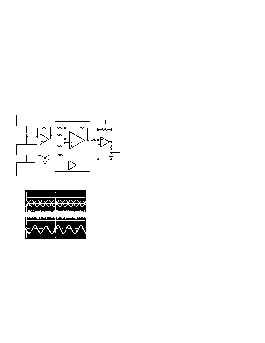
LOCK-IN AMPLIFIER APPLICATIONS
Lock-in amplification is a technique which is used to separate a
small, narrow band signal from interfering noise. The lock-in
amplifiers acts as a detector and narrow band filter combined.
Very small signals can be detected in the presence of large
amounts of uncorrelated noise when the frequency and phase of
the desired signal are known.
The lock-in amplifier is basically a synchronous demodulator
followed by a low-pass filter. An important measure of performance
in a lock-in amplifier is the dynamic range of its demodulator.
The schematic diagram of a demonstration circuit which exhibits
the dynamic range of an AD630 as it might be used in a lock-in
amplifier is shown in Figure 14. Figure 15 is an oscilloscope
photo showing the recovery of a signal modulated at 400 Hz
from a noise signal approximately 100,000 times larger; a dynamic
range of 100 dB.
A
B
10k
100R
C
OUTPUT
LOW PASS
FILTER
A
B
C
R
100R
AD630
10k
5k
2.5k
2.5k
20
19
17
1
16
AD542
13
AD542
14
10
9
CLIPPED
BAND-LIMITED
WHITE NOISE
100dB
ATTENUATION
0.1Hz
MODULATED
400Hz
CARRIER
CARRIER
PHASE
REFERENCE
15
Figure 14. Lock-In Amplifier
100
90
10
0%
5V
5V
5s
5mV
MODULATED SIGNAL (A)
(UNATTENUATED)
ATTENUATED SIGNAL
PLUS NOISE (B)
OUTPUT
Figure 15. Lock-In Amplifier Waveforms
The test signal is produced by modulating a 400 Hz carrier with
a 0.1 Hz sine wave. The signals produced, for example, by
chopped radiation (IR, optical, etc.) detectors may have similar
low frequency components. A sinusoidal modulation is used for
clarity of illustration. This signal is produced by a circuit similar
to Figure 9b and is shown in the upper trace of Figure 15. It is
attenuated 100,000 times normalized to the output, B, of the
summing amplifier. A noise signal which might represent, for
example, background and detector noise in the chopped radia-
tion case, is added to the modulated signal by the summing
amplifier. This signal is simply band limited clipped white noise.
Figure 15 shows the sum of attenuated signal plus noise in the
center trace. This combined signal is demodulated synchro-
nously using phase information derived from the modulator,
and the result is low-pass filtered using a 2-pole simple filter
which also provides a gain of 100 to the output. This recovered
signal is the lower trace of Figure 15.
The combined modulated signal and interfering noise used for
this illustration is similar to the signals often requiring a lock-in
amplifier for detection. The precision input performance of the
AD630 provides more than 100 dB of signal range and it
dynamic response permits it to be used with carrier frequencies
more than two orders of magnitude higher than in this example.
A more sophisticated low-pass output filter will aid in rejecting
wider bandwidth interference.
REV. D
AD630
11
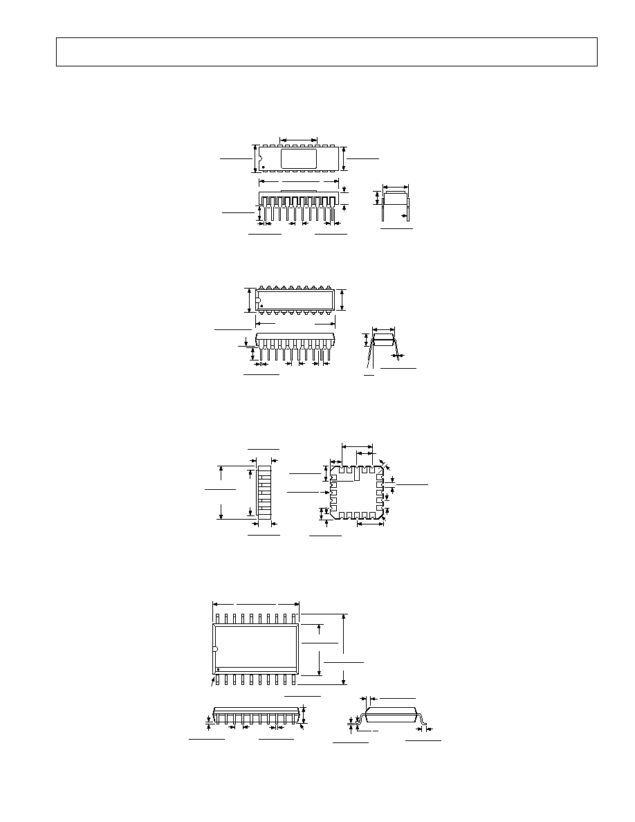
20-Lead Ceramic DIP (D-20)
20
1
10
11
0.280 (7.11)
0.300 (7.62)
0.430 (10.16)
0.300 (7.62)
0.320 (8.13)
0.085 (2.16)
0.150 (3.81)
0.210 (5.33)
0.990 (25.15)
1.010 (25.65)
0.10
(2.54)
0.015 (0.38)
0.020 (0.51)
0.040 (1.01)
0.054 (1.37)
0.300 (7.62)
0.300
(7.62)
0.008 (0.20)
0.012 (0.30)
20-Lead Plastic DIP (N-20)
20
1
10
11
1.070 (27.18)
0.250
(6.350)
TYP
0.180
(4.572)
MAX
0.300 (7.62)
TYP
0.025 (0.635)
0.045 (1.143)
0.015 (0.381)
0.021 (0.533)
0.125 (3.18)
MIN
0.100
(2.54)
TYP
0.033 (0.838)
TYP
0.310
(7.874)
TYP
15
0
0.008 (0.203)
0.014 (0.356)
LCC (E-20A)
1
20
4
9
8
13
19
14
3
18
BOTTOM
VIEW
0.028 (0.71)
0.022 (0.56)
45° TYP
0.015 (0.38)
MIN
0.055 (1.40)
0.045 (1.14)
0.050 (1.27)
BSC
0.075 (1.91)
REF
0.011 (0.28)
0.007 (0.18)
R TYP
0.095 (2.41)
0.075 (1.90)
0.100 (2.54) BSC
0.200 (5.08)
BSC
0.150 (3.81)
BSC
0.075
(1.91)
REF
0.358 (9.09)
0.342 (8.69)
SQ
0.358
(9.09)
MAX
SQ
0.100 (2.54)
0.064 (1.63)
0.088 (2.24)
0.054 (1.37)
20-Lead Small Outline Package
(R-20)
0.0125 (0.32)
0.0091 (0.23)
8
0
0.0291 (0.74)
0.0098 (0.25)
45
0.0500 (1.27)
0.0157 (0.40)
SEATING
PLANE
0.0118 (0.30)
0.0040 (0.10)
0.0192 (0.49)
0.0138 (0.35)
0.1043 (2.65)
0.0926 (2.35)
0.0500
(1.27)
BSC
20
11
10
1
0.4193 (10.65)
0.3937 (10.00)
0.2992 (7.60)
0.2914 (7.40)
PIN 1
0.5118 (13.00)
0.4961 (12.60)
OUTLINE DIMENSIONS
Dimensions shown in inches and (mm).

REV. D
12
Location
Page
Data Sheet changed from REV. C to REV. D.
Changes to SPECIFICATIONS Table . . . . . . . . . . . . . . . . . . . . . . . . . . . . . . . . . . . . . . . . . . . . . . . . . . . . . . . . . . . . . . . . . . . . . . . 2
Changes to THERMAL CHARACTERISTICS . . . . . . . . . . . . . . . . . . . . . . . . . . . . . . . . . . . . . . . . . . . . . . . . . . . . . . . . . . . . . . . . 3
Changes to ORDERING GUIDE . . . . . . . . . . . . . . . . . . . . . . . . . . . . . . . . . . . . . . . . . . . . . . . . . . . . . . . . . . . . . . . . . . . . . . . . . . . 3
Changes to PIN CONFIGURATIONS . . . . . . . . . . . . . . . . . . . . . . . . . . . . . . . . . . . . . . . . . . . . . . . . . . . . . . . . . . . . . . . . . . . . . . . 3
Changes to OUTLINE DIMENSIONS . . . . . . . . . . . . . . . . . . . . . . . . . . . . . . . . . . . . . . . . . . . . . . . . . . . . . . . . . . . . . . . . . . . . . 10
C0078406/01(D)
PRINTED IN U.S.A.
AD630Revision History