 | ÐлекÑÑоннÑй компоненÑ: AD6402ARS | СкаÑаÑÑ:  PDF PDF  ZIP ZIP |
Äîêóìåíòàöèÿ è îïèñàíèÿ www.docs.chipfind.ru
REV. 0
Information furnished by Analog Devices is believed to be accurate and
reliable. However, no responsibility is assumed by Analog Devices for its
use, nor for any infringements of patents or other rights of third parties
which may result from its use. No license is granted by implication or
otherwise under any patent or patent rights of Analog Devices.
a
AD6402
One Technology Way, P.O. Box 9106, Norwood, MA 02062-9106, U.S.A.
Tel: 617/329-4700
World Wide Web Site: http://www.analog.com
Fax: 617/326-8703
© Analog Devices, Inc., 1997
IF Transceiver Subsystem
FEATURES
On-Chip Regulator
PLL Demodulator
On-Chip VCO
No Trims
Excellent Sensitivity
28-Lead SSOP Package
APPLICATIONS
DECT/PWT/WLAN
TDMA FM/FSK Systems
GENERAL DESCRIPTION
The AD6402 is a complete transceiver subsystem for use in
high bit rate radio systems employing FM or FSK modulation.
It is optimized for use in time domain multiple access (TDMA)
systems with communications rates of approximately 1 MBPS.
The AD6402 integrates key functions, including VCOs and a
low drop-out voltage regulator. The AD6402 operates directly
from an unregulated battery supply of 3.1 V to 4.5 V and pro-
vides a regulated voltage output which can be used for VCO
supply regulation on a companion RF chip such as the AD6401.
The AD6402 transceiver consists of a mixer, integrated IF
bandpass filter, IF limiter with RSSI detection, VCO, PLL
demodulator and a low dropout voltage regulator. On receive, it
downconverts an IF signal in the 110 MHz range to a second
IF frequency, this frequency being determined by the demodu-
lator reference divide ratios. It then filters, amplifies, and de-
modulates this signal. The AD6402 provides a filtered baseband
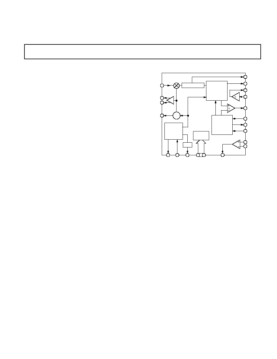
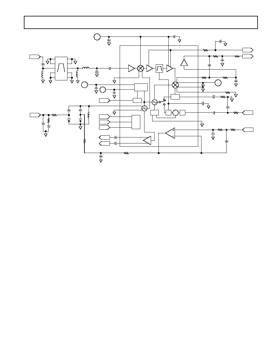
FUNCTIONAL BLOCK DIAGRAM
PLL
DEMOD
1
IF
VCO
VOLTAGE
REGULATOR
V
REF
MODE
CONTROL
DC
OFFSET
COMP
LIMITER/FILTER
2
AD6402
RSSI
CFILT
DOUT
DFILP
PLLOUT
FMMOD2
FMMOD1
IFIN
TXOUT
TXOUTB
VCO
VREG VBATT SLREF
CTL1...3
MODOUT
REFSEL
COFF
REFIN
data output. On transmit, it accepts a Gaussian Frequency Shift
Keying (GFSK) baseband signal, low-pass filters the signal if
required using the on-chip op amp and modulates the IF VCO
by varying the bias voltage on an off-chip varactor diode used in
the tank circuit.
The AD6402 has multiple power-down modes to maximize
battery life. It operates over a temperature range of 25
°
C to
+85
°
C and is packaged in a JEDEC standard 28-lead small-
shrink outline (SSOP) surface-mount package.

2
REV. 0
AD6402SPECIFICATIONS
AD6402ARS
Parameter
Conditions
Min
Typ
Max
Units
IF BANDPASS FILTER
Center Frequency Rejection
REFIN = 13.824 MHz, REFSEL <0.2 V
CC
20.736
MHz
F
O
±
3.0 MHz
7
dBc
F
O
±
4.7 MHz
13
dBc
F
O
±
6.0 MHz
16
dBc
Stop Band Rejection
30
dBc
RECEIVER
Sensitivity
FM Modulated 576 kHz, FM Deviation 288 kHz
80
dBm
BT = 0.5, Demod Output SNR = 10 dB, R
S
= 150
RSSI
Low
V
OUT
= 0.2 V, R
S
= 150
85
dBm
High
V
OUT
= 1.8 V, R
S
= 150
5
dBm
Slope
See Figure 4
20
mV/dB
Output Impedance
4
k
DEMODULATOR
Gain
At Data Filter Output
1.2
1.55
V/MHz
Offset
Referred to SLREF
200
+200
mV
Lock Time
From SLEEP Mode
200
µ
s
From RXLOCK Mode
20
µ
s
DATA FILTER OP AMP
Gain
2
Slew Rate
C
LOAD
= 30 pF
8
V/
µ
s
Gain Bandwidth
C
LOAD
= 30 pF
15
MHz
Output Swing Low
0.2
V
Output Swing High
V
CC
0.2
V
Output Impedance
50
IF VCO
Frequency
Note 1
131
MHz
SSB Phase Noise
@ 5 MHz Offset
139
dBc/Hz
Output Power
Differential R
LOAD
= 300
12
dBm
2nd Harmonic
22
dB
3rd Harmonic
24
dB
TRANSMIT FILTER OP AMP
Open Loop Gain
75
dB
Unity Gain Bandwidth
C
LOAD
= 30 pF
12
MHz
Output Slew Rate
C
LOAD
= 30 pF
5
V/
µ
s
Minimum Input Voltage
1
V
Maximum Input Voltage
V
CC
0.2
V
Minimum Output Voltage
0.2
V
Maximum Output Voltage
V
CC
0.2
V
POWER CONTROL
Logical High Threshold
0.8
×
V
CC
V
Logical Low Threshold
0.2
×
V
CC
V
Turn-On Response Time
V
CC
Steady State
0.5
µ
s
VOLTAGE REFERENCE
SLREF
1.3
1.5
V
SUPPLY REGULATOR
Output Voltage
For Battery Voltages from 3.1 V to 4.5 V
2.75
2.95
V
Turn-On Time
1 mV Settling, C
LOAD
= 100 nF
200
µ
s
Line Regulation
200 mV Battery Step; 5 mV Settling
1
µ
s
Load Regulation
10
µ
A to 30 mA Step; 5 mV Settling
200
µ
s
POWER SUPPLY
All V
CC
at 2.85 V
Supply Current
RXLOCKP
30
mA
RXLOCK
17
mA
RXDEMOD
26
mA
TRANSMIT
6
mA
STANDBY
300
µ
A
SLEEP
10
µ
A
NOTES
1
Using test tank circuit as shown.
Specifications subject to change without notice.
AD6402
3
REV. 0
WARNING!
ESD SENSITIVE DEVICE
CAUTION
ESD (electrostatic discharge) sensitive device. Electrostatic charges as high as 4000 V readily
accumulate on the human body and test equipment and can discharge without detection.
Although the AD6402 features proprietary ESD protection circuitry, permanent damage may
occur on devices subjected to high energy electrostatic discharges. Therefore, proper ESD
precautions are recommended to avoid performance degradation or loss of functionality.
RECOMMENDED OPERATING CONDITIONS
VBAT . . . . . . . . . . . . . . . . . . . . . . . . . . . . . . . . . 3.1 V4.5 V
IFVCC1, IFVCC2, PLLVCC . . . . . . . . . . . . . . . . . . . .2.85 V
Operating Temperature Range . . . . . . . . . . . 25
°
C to +85
°
C
ABSOLUTE MAXIMUM RATINGS*
Supply Voltage . . . . . . . . . . . . . . . . . . . . . . . . . . . . . . . +5.5 V
Storage Temperature Range . . . . . . . . . . . . 65
°
C to +150
°
C
Lead Temperature, Soldering (60 sec) . . . . . . . . . . . . +300
°
C
*Stresses above those listed under Absolute Maximum Ratings may cause perma-
nent damage to the device. This is a stress rating only; functional operation of the
device at these or any other conditions above those indicated in the operational
section of this specification is not implied. Exposure to absolute maximum rating
conditions for extended rating conditions for extended periods may affect device
reliability.
Thermal Characteristics:
28-lead SSOP package:
JA
= 109
°
C/W.
ORDERING GUIDE
Temperature
Package
Model
Range
Description
AD6402ARS
25
°
C to +85
°
C
28-Lead SSOP
AD6402ARS-REEL
25
°
C to +85
°
C
28-Lead SSOP
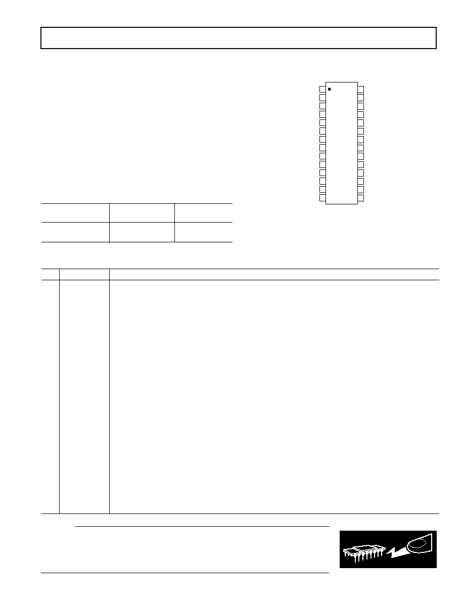
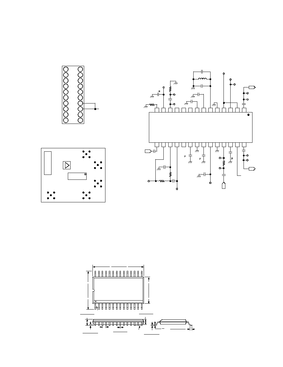
PIN CONFIGURATION
14
13
12
11
17
16
15
20
19
18
10
9
8
1
2
3
4
7
6
5
TOP VIEW
(Not to Scale)
28
27
26
25
24
23
22
21
AD6402
TXOUTB
IFIN
IFVCC1
REFSEL
TXOUT
MODOUT
FMMOD2
FMMOD1
IFVCC2
RSSI
IFGND
VCOGND
VCO
VREG
VBAT
CTL3
CTL2
SLREF
PLLVCC
PLLGND
CTL1
CFILT
COFF
REXT
DOUT
REFIN
PLLOUT
DFILP
PIN FUNCTION DESCRIPTIONS
Pin
Mnemonic
Function
1
TXOUTB
Transmit IF VCO Buffer Inverting Output
2
MODOUT
Frequency Modulator Filter Op Amp Output
3
FMMOD2
Frequency Modulator Filter Op Amp Noninverting input
4
FMMOD1
Frequency Modulator Filter Op Amp Inverting input
5
VCOGND
IF VCO Ground
6
VCO
IF VCO Tank Connection
7
VREG
Regulated Supply Output for RF VCO (Supplies Internal IF VCO, Mode Control, Bandgap Reference,
and COFF Buffer)
8
VBAT
Battery Supply Voltage Input to Internal Regulator and COFF Charge Pump
9
CTL3
Mode Control Input 3, CMOS Logical Level
10
CTL2
Mode Control Input 2, CMOS Logical Level
11
CTL1
Mode Control Input 1, CMOS Logical Level
12
CFILT
PLL Demodulator Loop Filter Capacitor
13
COFF
PLL Demodulator Frequency Offset Voltage Track/Hold Capacitor
14
REXT
External Current-Setting Resistor
15
REFIN
Baseband Reference Frequency Input, 100 mV p-p, AC Coupled
16
PLLOUT
PLL Demodulator Output
17
DFILP
Data Filter Voltage-Follower Input
18
DOUT
Data Filter Voltage-Follower Output
19
SLREF
PLL Demodulator Output DC Reference Voltage
20
PLLVCC
PLL Demodulator and Data Filter Supply Input
21
PLLGND
PLL Demodulator and Data Filter Ground
22
IFVCC2
IF Limiter Supply Input 1
23
RSSI
RSSI Output
24
IFGND
IF Stage, Mixer, Band Pass Filter, IF VCO Buffer, Tx Op Amp, Mode Control, and Regulator Ground
25
IFIN
IF Mixer Input, Z
O
= 150 Z
26
IFVCC1
IF Mixer, Limiter 1, IF Filter, IF VCO Buffer
27
REFSEL
Reference Frequency Select; IF = 1.5
×
or 2.5
×
Reference Frequency, CMOS Logical Level Input
28
TXOUT
Transmit IF VCO Buffer Output
AD6402
4
REV. 0
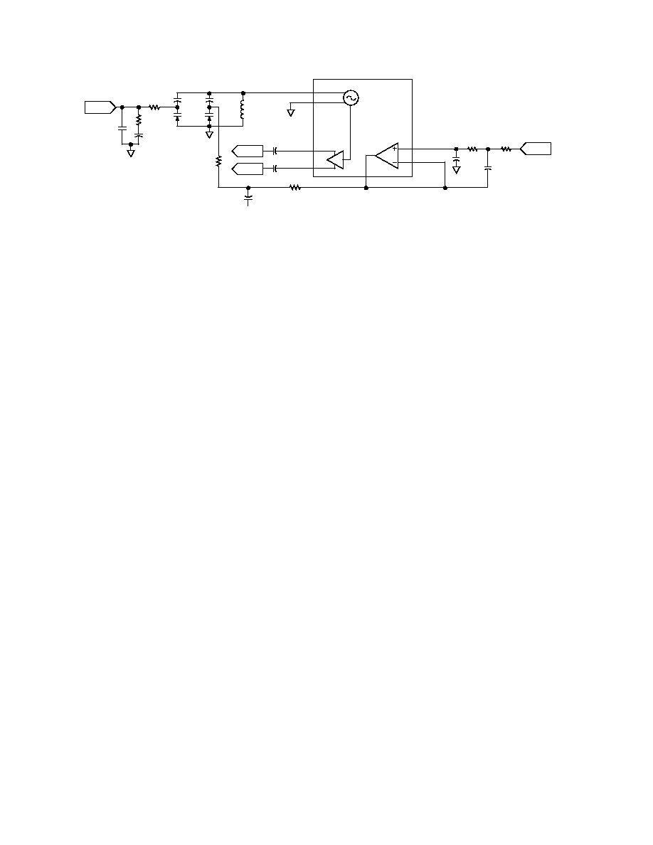
AD6402
VCO
VCOGND
TXOUT
TXOUTB
MODOUT
FMMOD2
FMMOD1
1nF
1nF
SMV
1204-36
39nH
8pF
47pF
1.2k
4.7nF
1nF
SMV
1204-37
240
150pF
VCCI
330
100pF
330
180pF
330
TXMOD
TXIF+
TXIF
V
TUNE
Figure 1.
OVERVIEW
The AD6402 forms the basis of a highly integrated RF trans-
ceiver with the benefits of increased sensitivity and wide dy-
namic range that a dual-conversion architecture provides. The
IC contains a low dropout voltage regulator to isolate the IF and
demodulator VCOs from variation in the battery voltage, such
as power-supply transients caused by the PA. The AD6402 also
provides control circuitry that allows subcircuits to be turned off
and on as necessary to minimize power consumption.
Operation During Receive
The AD6402 contains the second mixer, integrated second-IF
bandpass filter, logarithmic-limiting amplifier, and PLL de-
modulator. A SAW IF bandpass filter is usually required at the
IF input in order to provide channel selectivity.
The placement of the SAW filter in the signal path between
the AD6402 and the RF section and the partitioning of the
receiver's RF and IF receive circuits minimizes the leakage
around the SAW filter and maximizes the RF to IF isolation.
The output of the SAW filter enters the AD6402 via the second
downconversion mixer. This mixer is a high gain, doubly-
balanced Gilbert-cell type. The mixer downconverts the signal
to the second IF, which is 1.5
×
or 2.5
×
the reference frequency.
This multiple is determined by the state of the REFSEL pin. An
on-chip two section bandpass filter provides additional selectiv-
ity to provide attenuation of adjacent channels. The VCO con-
trol voltage output of the PLL demodulator tunes this filter to
the second IF.
The bandpass filter's output enters a successive-detection loga-
rithmic-limiting IF amplifier. The RSSI detectors are distrib-
uted across the entire IF strip, including the mixer, and provide
80 dB RSSI range. The IF strip's limiting gain also exceeds 80
dB. The RSSI signal is low-pass filtered and proceeds off-chip
to the baseband subsystem. The limited output of the logarith-
mic amplifier enters a PLL demodulator, which provides de-
modulation of the received signal. The PLL uses an integrated
VCO with no external components.
Operation During Transmit
The transmit signal path consists of a low-pass filter that can be
user configured for antialiasing of a baseband transmit signal.
An IF VCO, which should be tuned to a frequency equal to the
receive IF frequency plus the desired demodulator input fre-
quency, may be open-loop modulated by the transmit signal for
FM and FSK schemes. The receive IF mixer uses high side
mixing and therefore the IF VCO should be set to a frequency
equal to the sum of the IF frequency plus the frequency of the
PLL demodulator input as defined by the reference clock
divider ratios.
The transmit IF VCO uses an external tank circuit. This signal
is upconverted to the transmit frequency in the RF mixer sec-
tion of the radio. Using a transmit IF VCO prevents two prob-
lems: feedback from the PA at the RF frequency does not cause
distortion in the modulating circuit because the frequencies are
widely separated and the IF tank circuit can be optimized for
modulation linearity.
The output of the transmit VCO passes through buffer amplifier
and leaves the AD6402 via an optional LC filter between the RF
and IF ICs. The output of the LC filter may then be fed to a
transmit upconversion mixer for conversion to the final RF
frequency.
Onboard Voltage Regulation
The AD6402 contains a low dropout voltage regulator to spe-
cifically isolate the VCOs and synthesizer from the voltage
"kick" that occurs when a power amplifier switches on and the
battery voltage abruptly drops. The AD6402 uses an integral
vertical PNP pass transistor.
The regulator in the AD6402 IF IC supplies the voltage for the
VCOs on both the RF section and AD6402. The other sections
of the AD6402 should be powered from an independently regu-
lated source at 2.85 V. Since the VCOs are isolated from this
source, possible problems due to VCO supply pushing are con-
siderably reduced.
Frequency Control
The AD6402 requires an external synthesizer to provide the
control voltages for the tank circuit of the IF VCO. Normally
this will be the IF section of a dual synthesizer controlling both
IF and RF frequency generation.
It is recommended that the VCO on the RF section implement
the channel selection on transmit and receive; the VCO on the
AD6402 may therefore operate at a fixed frequency. This ac-
complishes two goals: first, the IF VCO being modulated can be
optimized for modulation linearity and the RF VCO can be
optimized for tuning range, and second, feedback from the PA
at will not couple into the modulating circuit to cause spurious
responses.
All key sections of the AD6402 may be powered up or down as
necessary to minimize power consumption and maximize
battery life.
AD6402
5
REV. 0
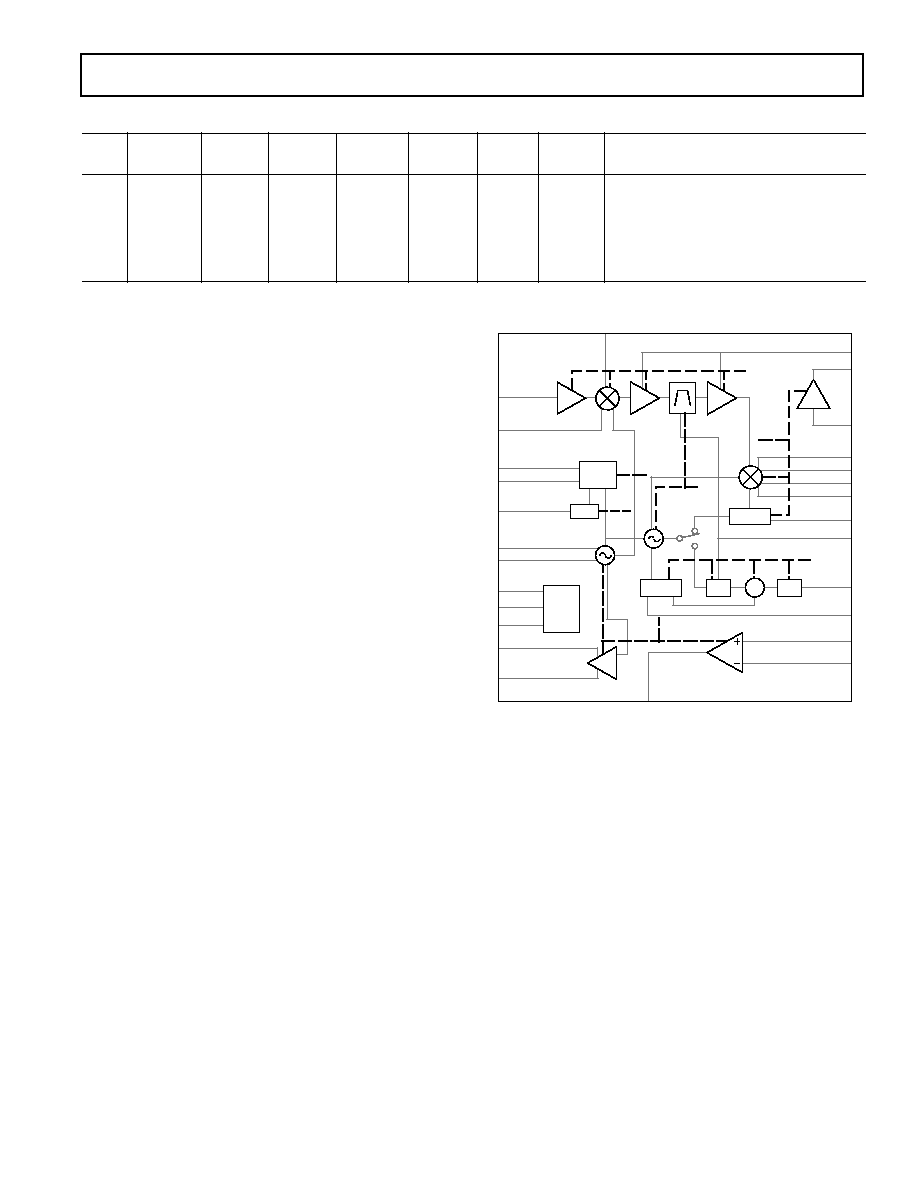
Table I. Power Management Functionality
PLL
PLL
PLL
TL1
CTL2
CTL3
BIAS
LOCK
DMOD
REF
REG
RX
VCO
MODE
0
0
0
OFF
OFF
SLEEP
0
0
1
OFF
ON
STANDBY
0
1
0
ON
ON
OFF
ON
ON
OFF
ON
RXLOCK
1
X
0
ON
OFF
ON
ON
ON
ON
ON
RXDMOD
1
0
1
OFF
OFF
OFF
ON
ON
OFF
ON
TRANSMIT
1
1
1
ON
ON
OFF
ON
ON
ON
ON
RXLOCKP
REF
RX
PLL DMOD
PLL BIAS
REF
REG
PLL LOCK
VCO
IFVCC1
IFVCC2
RSSI
DOUT
DFLIP
PLLOUT
PLLVCC
PLLGND
REXT
CFILT
REFSEL
FMMOD2
FMMOD1
MODOUT
TXOUTB
TXOUT
CTL1
CTL2
CTL3
VCOGND
VCO
SLREF
VREG
VBAT
IFGND
IFIN
COFF
REFIN
REG
CP
/2
CP
/3,/5
PD
Figure 2. Power Management Scheme
The AD6402 has six operating modes: SLEEP, STANDBY,
RXLOCK, RXDMOD, TRANSMIT and RXLOCKP. These
are summarized in Table I. The blocks referred to in Table I are
shown also in Figure 4. These modes are described as follows:
SLEEP:
The entire device is shut down.
STANDBY:
All functions except the regulator are shut down.
RXLOCK:
The device locks to a local reference clock using
the lock PLL. The lock charge pump and divid-
ers are powered up. The VCO is also powered up.
RXDMOD:
In this mode the lock charge pump and loop
dividers are shut down. The receive mixer, IF strip,
reference and demodulator are powered up.
TRANSMIT: This mode enables the VCO and transmit op
amp. The reference and regulator are also enabled.
RXLOCKP:
This mode may be used in a "prior to" timeslot,
i.e., the slot before the actual active receive
timeslot. In this mode, after lock has been
achieved in the RXLOCK mode, the receive
mixer, VCO and IF strip may then be indepen-
dently powered up from the demodulator loop.
This can result is power savings, since the de-
modulator may be powered down during the
IF VCO lock acquisition time.
AD6402
6
REV. 0
Demodulator Operation
The PLL itself uses two loops: one for rapid frequency acquisi-
tion and a second for demodulation. The first, or frequency-
acquisition loop, locks the VCO to a noninteger multiple of the
system clock, either 3/2 or 5/2 (using one fixed /2 and one pro-
grammable /3 or /5 divider). This allows not only a choice of IF
and system clocks but also prevents blocking of the receiver by
keeping integer multiples of the system clock out of the IF
passband.
Once locked, this loop voltage is stored on an external capacitor
and this sets the free-running frequency of the VCO during
demodulation. The first loop is opened and, using the second
loop and phase detector, the PLL compares the free-running
frequency of its VCO to the frequency of the incoming IF. The
VCO is then fast frequency locked, and slow phase locked to the
incoming IF. Preconditioning of the PLL to the local reference
clock facilitates the fast frequency lock to the received IF. The
PLL now generates a baseband voltage proportional to the fre-
quency deviation of the received signal.
The demodulator uses a third-order PLL to track the incoming
modulation signal. A simplified diagram of the demodulator is
shown in Figures 3a and 3b. The loop bandwidth and damping
factor can be adjusted by changing the values of C and R as
indicated. An internal pole is present on the demodulator loop
at approximately 9 MHz. For a loop
n
of 800 kHz, values of
910 pF and 330
respectively are optimum. The loop band-
width will approximately scale inversely as the square root of the
value of C. To preserve a satisfactory damping factor, R should
be adjusted linearly with the loop bandwidth. At low loop band-
widths however the value of C offset must also be increased to
enable the loop to lock to the reference frequency during prior
to receive time slots.
APPLICATIONS
The AD6402 is optimized for use in applications where a data
rate of the order of 1 megabit per second is required and the
modulation scheme employed is constant envelope, i.e., FM or
FSK. Because the demodulator uses a track and hold technique
that locks to an externally supplied reference clock, the device is
optimized for use in TDMA systems. If used in continuous
demodulation applications, the dc offset hold voltage on the
demodulator differential amplifier will ultimately leak away,
resulting in the average dc value of the demodulator output
eventually limiting against the supply rail. In a TDMA system,
the voltage on the capacitor is refreshed just before the active
PLLOUT
COFF
COFFSET
1.4k
500
34pF
VCO
220 A/RAD
CFILT
C
R
LIMITER
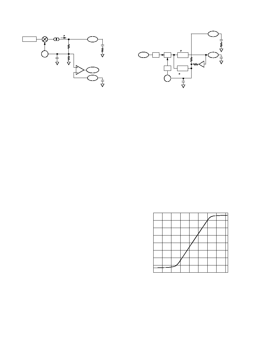
Figure 3a. Demodulator Block Diagram (Lock Mode)
COFF
COFFSET
CFILT
C
R
CPUMP
14 A/RAD
34pF
PD
/3,/5
VCO
/2
REFIN
160 A/RAD
CPUMP
Figure 3b. Demodulator Block Diagram (Dmod Mode)
timeslot, thereby enabling a very accurate dc offset compensa-
tion of system frequency errors.
The on-chip IF filter has been designed to provide some rejec-
tion of adjacent channel signals for channel bandwidths in the
1 MHz2 MHz range. This filter has the benefit of reducing the
contribution of broadband noise through the IF strip, hence
improving the overall sensitivity of the receiver for a given
demodulator output signal to noise ratio.
It is also possible to use the AD6402 in applications where non-
constant envelope modulation schemes are used, such as QPSK.
In these applications the amplitude information will be lost
through the limiting action of the IF strip, but in certain appli-
cations, sufficient eye-opening will be observed in the demodu-
lated signal to allow the use of hard decision bit-slicers as in the
FM or FSK case. The actual performance of the subsystem in
the presence of a QPSK signal will depend on factors such as bit
rate, modulation index and BT employed.
Figure 4 shows the RSSI response to a DECT signal at the IF
port. It can be seen from the plot that the AD6402 can detect
signals below 85 dBm and continues to detect linearly up to
and above 5 dBm.
INPUT POWER dBm
1.6
0.6
0
95
91
87
75
55
35
15
1.4
0.8
0.4
0.2
1.2
1.0
3
1
RSSI V
Figure 4. RSSI Response
Figure 5 shows an implementation for a DECT IF subsystem.
DECT is a 1.152 megabit/second radio, employing Gaussian
FSK modulation at a BT = 0.5 and uses a channel spacing of
1.728 MHz. It is a TDMA/TDD system. The IF frequency used
in this application is 110.592 MHz. The AD6402's flexible
power management scheme enables the part to operate at low
AD6402
7
REV. 0
supply current levels when not allocated to an active transmit or
receive timeslot in a TDMA system.. The respective transmit
and receive blocks can be turned on only as needed thereby
reducing power consumption and extending battery life of
handheld terminals.
The component selection in Figure 5 is explained as follows:
The IF input is driven from the output of a SAW filter via an
impedance matching circuit as shown. This matching minimizes
the insertion loss of the filter and follows the filter manufactur-
ers recommendations. The tank circuit shown uses two varactor
diodes. One diode (D3) is biased by the output of the IF PLL
loop filter and ensures that the IF VCO frequency is correctly
centered. The second diode is provided to enable a modulation
signal, which is generated at the output of the on-chip op amp
(MODOUT), to be coupled into the VCO tank and thereby
implement a modulation of the VCO frequency. In the case of
DECT, the IF VCO control loop is opened while the VCO is
being modulated by the transmit bit stream. The loop is opened
by tri-stating the output of the IF VCO PLL charge pump.
The exact component values used around the modulation am-
plifier will be determined by the amount of attenuation required
for suppression of baseband transmit spurii and images. These
artifacts are usually present if the baseband FSK signal is gener-
ated by a ROMDAC. In most instances a second or third order
Bessel or Butterworth filter will be required.
A capacitor to ground is required to be connected to COFF.
This capacitor stores the demodulator charge-pump voltage
required to lock the demodulator VCO to the reference fre-
quency. The dynamic response of the demodulator loop is con-
trolled by selection of the values for C45 and R22 which are
connected in series to CFILT. These components determine the
IFVCC1
IFVCC2
DOUT
DFILP
C71
1nF
C44
100nF
VRF
CP
REG
REF
CP
/3,/5
PD
RSSI
PLLOUT
PLLVCC
PLLGND
REXT
CFILT
REFSEL
FMMOD2
FMMOD1
MODOUT
TXOUTB
TXOUT
CTL1
CTL2
CTL3
VCOGND
VCO
SLREF
VREG
VBAT
IFGND
IFIN
COFF
REFIN
C30
150pF
R16
330
C28
1nF
C29
1nF
L11
39nH
C41
8pF
C42
47pF
R26
1.2k
C50
4.7nF
C25
1nF
R21
240
D2
D3
C43
100nF
VIF
C44
1nF
V
CC
12pF
C10
1nF
L7
100nH
L6
150nH
10
9
8
7
6
1
2
3
4
5
L5
150nH
C69
1nF
CP
C52
100pF
R28
330
C51
180pF
R32
330
R70
C32
100nF
C45
131nF
R22
330
C13
1nF
C31
R17
10k
C11
100pF
VRF
R10
2k
R9
1k
C14
68pF
C12
33pF
R30
2k
C58
47pF
RXBB
RSSI
C4
3.3nF
R8
4.7k
AD6402
SMV
1204-37
SMV
1204-36
TXIF
TXIF+
IFC0
IFC1
IFC2
VREF
V
TUNE
B4535
IFIN
TXBB
R35
4.7k
RCLK
Figure 5. Application Circuit for DECT GFSK Transceiver
transfer characteristic of the loop filter and hence the lock time,
settling time and bandwidth of the loop. REXT should use the
recommended value as shown.
Finally, the demodulator is followed by a voltage follower,
which is configured as a data filter. This data filter is used to
bandlimit the FM noise generated in the demodulator. It also
attenuates undesired adjacent channel interferers. The compo-
nent values chosen will be a trade-off between the amount of
band limiting required and attenuation of the in-band desired
signal.
DECT Application Circuit Notes (Figure 5)
1. Signal Description
VRF: Regulated Supply Voltage; Nominal Value 2.85 V.
V
CC
: Unregulated battery voltage; 3.1 V4.5 V
VTUNE: Synthesizer Control Voltage; Range dependent on
loop filter and synth charge pump compliance.
TXBB: Baseband transmit modulation voltage; typically
SLREF
±
0.7 V
RCLK: Reference clock for PLL demodulator; 13.824 MHz
(2nd IF frequency = (N/M)
×
Frclk where N = 3 or 5, and
M = 2. Maximum 2nd IF = c.26 MHz)
2. Typical IF input sensitivity referred to the input of SAW
filter for the above application will be 72 dBm.
3. TxBB filter is user configurable. In the above application, the
filter is implemented to remove images generated by ROM
DAC baseband signal generators. Other implementations are
possible including passive pulse shaping circuits which elimi-
nate the need for such filtering.
AD6402
8
REV. 0
OUTLINE DIMENSIONS
Dimensions shown in inches and (mm).
C3155127/97
PRINTED IN U.S.A.
28-Lead Small Shrink Outline Package
(RS-28)
28
15
14
1
0.407 (10.34)
0.397 (10.08)
0.311 (7.9)
0.301 (7.64)
0.212 (5.38)
0.205 (5.21)
PIN 1
SEATING
PLANE
0.008 (0.203)
0.002 (0.050)
0.07 (1.79)
0.066 (1.67)
0.0256
(0.65)
BSC
0.078 (1.98)
0.068 (1.73)
0.015 (0.38)
0.010 (0.25)
0.009 (0.229)
0.005 (0.127)
0.03 (0.762)
0.022 (0.558)
8
°
0
°
EVALUATION BOARD
An evaluation board is available for the AD6402. This board
facilitates test and measurement of the subsystem. Parameters
such as sensitivity, ACI, CCI, demodulator gain, demodulator
offset, etc., can be quickly evaluated using this board. Contact
20
18
16
14
12
10
8
6
4
2
19
17
15
13
11
9
7
5
3
1
PLLOUT
DOUT
SLREF
PLLVCC
GND
IFVCC2
RSSI
GND
IFVCC1
REFSEL
NC
MODIN
MODOUT
CTL1
CTL2
CTL3
VBATX
VBAT
GND
VREG
NC = NO CONNECT
J1
Figure 6. Evaluation Board Header
AD6402
20
1
J1
SYNTH IN
TXOUTB
TXOUT
IFIN
REFIN
NOTE:
SYNTH IN, TXOUTB, TXOUT, IFIN AND REFIN
CONNECTED VIA SMA CONNECTORS
Figure 7. Evaluation Board Connectors
your local ADI sales office or ADI representative for further
details on pricing and availability of the evaluation boards.
Header connections details are shown in Figure 6 and available
signals are shown in Figure 7. A schematic for the evaluation
board is shown in Figure 8.
8k
0.1 F
TP2
330
1000pF
TP
100nF
1nF
MODOUT
MODIN
REFIN
100pF
PLLOUT
91pF
2.2k
1.3k
0.01 F
0.01 F
2.2nF
RSSI
TO REFSEL
PIN 2
DC
CONNECTOR
100
IF INPUT
IFIN
DOUT
47pF
100pF
56pF
TP10
TXOUTB
14
13
12
11
10
9
8
7
6
5
4
3
2
1
15
16
17
18
19
20
21
22
23
24
25
26
27
28
TXOUTB
MODOUT
FMMOD2
FMMOD1
VCOGND
VCO
VREG
VBAT
CTL3
CTL2
CTL1
CFILT
COFF
REXT
IFIN
IFVCC1
REFSEL
TXOUT
IFVCC2
RSSI
IFGND
SLREF
PLLVCC
PLLGND
DOUT
REFIN
PLLOUT
DFILP
AD6402
TP
3pF
33nH
33pF
TP11
TP9
56pF
TXOUT
TP7
TP8
0.01
F
TP5
TP6
Figure 8. Evaluation Board Schematic