 | ÐлекÑÑоннÑй компоненÑ: AD6426XB | СкаÑаÑÑ:  PDF PDF  ZIP ZIP |
Äîêóìåíòàöèÿ è îïèñàíèÿ www.docs.chipfind.ru
a
Enhanced GSM Processor
Preliminary Technical Information
AD6426
This Information applies to a product under development. Its characteristics and specifications are subject to change without notice. Analog Devices assumes no
obligation regarding future manufacture unless otherwise agreed to in writing. No responsibility is assumed by Analog Devices for its use; nor for any
infringements of patents or other rights of third parties which may result from its use. No license is granted by implication or otherwise under any patent or patent
rights of Analog Devices.
Revision Preliminary 2.3 (June 9, ´98)
- 1 -
Confidential Information
FEATURES
Complete Single Chip GSM Processor
Channel Codec Subsystem including
Channel Coder/Decoder
Interleaver/De-interleaver
Encryption/Decryption
Control Processor Subsystem including
16-bit Control Processor (H8/300H)
Parallel and Serial Display Interface
Keypad Interface
EEPROM Interface
SIM-Interface
Universal System Connector Interface
Interface to AD6425
Control of Radio Subsystem
Programmable backlight duty cycle
Real Time Clock with Alarm
Battery ID Chip Interface
DSP Subsystem including
16-bit DSP with ROM coded firmware for
Full rate Speech Encoding/Decoding (GSM 06.10)
Enhanced Full Rate Speech
Encoding/Decoding (GSM 06.60)
Equalization with 16-state Viterbi (Soft Decision)
DTMF and Call Progress Tone Generation
Power Management of Mobile Radio
Slow Clocking scheme for low Idle Mode current
Ultra Low Power Design
On-chip GSM Data Services up to 14.4 kbit/s
JTAG Test Interface
2.4V to 3.3V Operating Voltage
144-Lead LQFP and 144-Lead PBGA packages
APPLICATIONS
GSM 900 / DCS1800 / PCS1900 Mobile Stations (MS)
Compliant to Phase 1 and Phase 2 specifications
GENERAL DESCRIPTION
The AD6426 Enhanced GSM Processor (EGSMP) is the
central component of the highly integrated AD20msp425 GSM
Chipset. Offering a low total chip count, low bill of materials
cost and long talk and standby times, the chipset offers
designers a straightforward route to a highly competitive
product in the GSM/DCS1800 market.
The EGSMP performs all the baseband functions of the Layer
1 processing of the GSM air interface. This includes all data
encoding and decoding processes as well as timing and radio
sub-system control functions.
The EGSMP supports full rate and enhanced full rate speech
traffic as well as a full range of data services including F14.4.
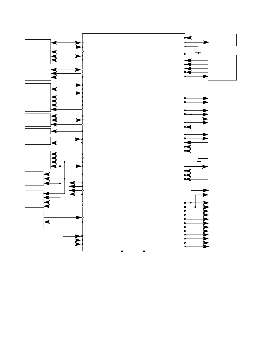
CONTROL
PROCESSOR
DSP
CHANNEL
EQUALIZER
SPEECH
CODEC
CHANNEL
CODEC
KEYPAD /
BACKLIGHT
INTERFACE
ACCESSORY
INTERFACE
RADIO
INTERFACE
SIM
INTERFACE
MEMORY
INTERFACE
UNIVERSAL
SYSTEM CONN.
INTERFACE
EEPROM
INTERFACE
TEST
INTERFACE
VOICEBAND /
BASEBAND
CODEC
INTERFACE
DISPLAY
INTERFACE
Figure 1. Functional Block Diagram
In addition, the EGSMP supports both A5/1 and A5/2
encryption algorithms as well as operation in non-encrypted
mode.
The EGSMP integrates a high performance 16-bit
microprocessor (Hitachi H8/300H), that supports all the GSM
terminal software, including Layer 1, 2 and 3 of the GSM
protocol stack, the MMI and applications software such as
data services, test and maintenance.
The use of the standard H8 processor allows the use of HIOS,
the Hitachi real time kernel, as well as a full range of software
development tools including C compilers, debuggers and in-
circuit emulators. The EGSMP also integrates a high
performance 16-bit Digital Signal Processor (DSP), which
provides speech transcoding and supports all audio functions
in both transmit and receive. In receive it equalizes the
received signal using a 16-state (Viterbi) soft decision
equalizer.
The EGSMP interfaces with all the peripheral sub-systems of
the terminal, including the keypad, memories, display driver,
SIM, DTE and DTA data services interface and radio. It also
has a general purpose interface that can be used to support an
external connection to a car kit or battery charger.
The EGSMP interfaces with the AD6425 or the AD6421
Voiceband/Baseband Codec through a dedicated serial port.
ORDERING GUIDE
Model
Temperature Range
Package
AD6426XST
-25°C to +85°C
144-Lead LQFP
AD6426XB
-25°C to +85°C
144-Lead PBGA
Preliminary Technical Information
AD6426
This Information applies to a product under development. Its characteristics and specifications are subject to change without notice. Analog Devices assumes no
obligation regarding future manufacture unless otherwise agreed to in writing. No responsibility is assumed by Analog Devices for its use; nor for any
infringements of patents or other rights of third parties which may result from its use. No license is granted by implication or otherwise under any patent or patent
rights of Analog Devices.
Revision Preliminary 2.3 (June 9, ´98)
- 2 -
Confidential Information
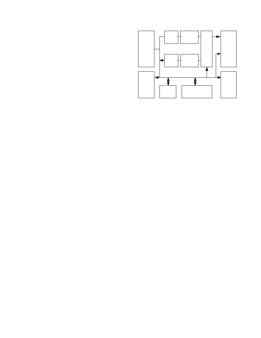
ENHANCED
GSM
PROCESSOR
AD6426
VDD(10) GND(10)
VBC / EVBC
AD6421 / 25
MCLK
RESET
ASDI
ASDIFS
ASDOFS
ASCLK
ASDO
BSDI
BSDIFS
BSCLK
BSDO
BSDOFS
MODE
VSDI
VSDO
VSCLK
VSFS
RXON
TXON
CLKOUT
VBCRESET
ASDO
ASOFS
ASCLK
ASDI
BSDO
BSOFS
BSCLK
BSDI
BSIFS
VSDO
VSDI
VSCLK
VSFS
RXON
TXENABLE
TXPHASE
TXPA
CALIBRATERADIO
RADIOPWRCTL
SYNTHEN0
SYNTHEN1
SYNTHDATA
SYNTHCLK
AGCA
AGCB
RADIO
VCTCXO
JTAGEN
TCK
TMS
TDI
TDO
JTAG
PORT
IRQ6
RESET
BOOTCODE
SYSTEM
CONNECTOR
ACCESSORY
SIM
SIMCARD
SIMDATAOP
SIMDATAIP
SIMCLK
SIMRESET
SIMPROG
SIMSUPPLY
EEPROM
EEPROMEN
EEPROMDATA
EEPROMCLK
DISPLAY
FLASH
ROM
SRAM
FLASHPWD
ROMCS
ADD [20:0]
DATA [15:0]
RAMCS
RD
WR
HWR
LWR
LCDCTL
DISPLAYCS
BACKLIGHT
BACKLIGHT
KEYPADROW [5:0]
KEYPADCOL [3:0]
KEYPAD
GPIO [9:0]
GPCS
GPPWRCTL
USCRI
USCRX
USCTX
USCCTS
USCRTS
CLKIN
OSC13MON
OSCIN
OSCOUT
POWER
SUB-
SYSTEM
VDDRTC
PWRON
Figure 2. External Interfaces of the AD6426

Preliminary Technical Information
AD6426
This Information applies to a product under development. Its characteristics and specifications are subject to change without notice. Analog Devices assumes no
obligation regarding future manufacture unless otherwise agreed to in writing. No responsibility is assumed by Analog Devices for its use; nor for any
infringements of patents or other rights of third parties which may result from its use. No license is granted by implication or otherwise under any patent or patent
rights of Analog Devices.
Revision Preliminary 2.3 (June 9, ´98)
- 3 -
Confidential Information
Table of Contents
GENERAL DESCRIPTION ...................................................1
PIN FUNCTIONALITY ( Normal Mode) ...............................4
OVERVIEW..........................................................................7
FUNCTIONAL PARTITIONING ...........................................7
Channel Codec Sub-System ...............................................7
Processor Sub-System ........................................................8
DSP Sub-System................................................................8
Speech Transcoding .......................................................8
Equalization...................................................................8
Audio Control ................................................................8
Tone Generation ............................................................8
Automatic Frequency Control (AFC) ..............................8
Automatic Gain Control (AGC) ......................................8
REGISTERS..........................................................................9
GENERAL CONTROL........................................................14
Clocks .............................................................................14
Slow Clocking .................................................................14
Real Time Clock and Alarm.............................................14
Reset ...............................................................................15
Interrupts .........................................................................15
NMI.................................................................................15
Wait ................................................................................16
Automatic Booting ...........................................................16
Power Control..................................................................16
INTERFACES .....................................................................16
Memory Interface.............................................................16
EEPROM Interface ..........................................................16
SIM Interface...................................................................17
Accessory Interface ..........................................................17
Universal System Connector Interface ..............................18
Operating modes of the USC............................................18
Buffered UART Mode (Booting/Data Services)................18
Keypad / Backlight / Display Interface .............................19
Battery ID Interface..........................................................20
EVBC Interface ...............................................................20
Radio Interface ................................................................22
Dual Band Control .......................................................22
Tx Timing Control .......................................................23
Rx Timing Control .......................................................24
Synthesizer Control ......................................................24
AGC Control................................................................25
TEST INTERFACE .............................................................27
JTAG Port....................................................................27
Debug Port Interface ....................................................29
MODES OF OPERATION...................................................29
Normal Mode (Mode A) ..................................................29
Emulation Mode (Mode D) ..............................................29
FEATURE MODES.............................................................30
DAI Mode........................................................................30
High Speed Logging.........................................................30
SPECIFICATIONS ..............................................................32
General............................................................................32
ABSOLUTE MAXIMUM RATINGS ...............................32
TIMING CHARACTERISTICS............................................33
Clocks .............................................................................33
Memory Interface.............................................................34
Radio Interface ................................................................35
High Speed Logging Interface ..........................................36
Data Interface ..................................................................37
Test Interface...................................................................38
EVBC Interface ASPORT ................................................39
EVBC Interface BSPORT ................................................40
EVBC Interface VSPORT ................................................41
Parallel Display Interface .................................................42
Serial Display Interface....................................................43
PACKAGING......................................................................44
LQFP Pin Locations.........................................................44
PBGA Pin Locations ........................................................45
LQFP Outline Dimensions ...............................................47
PBGA Outline Dimensions ..............................................48

Preliminary Technical Information
AD6426
This Information applies to a product under development. Its characteristics and specifications are subject to change without notice. Analog Devices assumes no
obligation regarding future manufacture unless otherwise agreed to in writing. No responsibility is assumed by Analog Devices for its use; nor for any
infringements of patents or other rights of third parties which may result from its use. No license is granted by implication or otherwise under any patent or patent
rights of Analog Devices.
Revision Preliminary 2.3 (June 9, ´98)
- 4 -
Confidential Information
PIN FUNCTIONALITY ( Normal Mode)
Group
Pin Name
Pins
I/O
Default / Alternative Function(s) *
General
CLKIN
1
I
13 MHz Clock Input
RESET
1
I
Reset input
IRQ6
1
I / I
Interrupt Request # 6 / Non-Maskable Interrupt (NMI) *
OSC13MON
1
O
13 MHz Oscillator Power Control Signal
BOOTCODE
1
I
Boot Code Enable
VDD
10
Supply Voltage
GND
10
Ground
Memory
ADD19 : 0
20
O
Processor Address Bus
Interface
GPO10
1
O / O
General Purpose Output 10 / Address (20) *
DATA15 : 0
16
I/O
Processor Data Bus
RD
1
O
Processor Read Strobe
HWR
1
O
Processor High Write Strobe / Upper Byte Strobe
LWR
1
O
Processor Low Write Strobe / Lower Byte Strobe
WR
1
O
Processor Write Strobe
FLASHPWD
1
O / I /
O
FLASH Power Down / WAIT / General Purpose Output
11*
RAMCS
1
O
External RAM Chip Select
ROMCS
1
O
External ROM Chip Select
SIM
SIMCARD
1
I /
I/O
SIM Card Detect / General Purpose I/O 16 *
Interface
SIMDATAOP
1
O
SIM Data Output
SIMDATAIP
1
I
SIM Data Input
SIMCLK
1
O
SIM Clock
SIMRESET
1
O
SIM Reset
SIMPROG
1
O /
I/O
SIM Program Enable / General Purpose I/O 15 *
SIMSUPPLY
1
O
SIM Supply Enable
EEPRROM
EEPROMDATA
1
I/O
EEPROM Data
Interface
EEPROMCLK
1
O
EEPROM Clock / High Speed Logger Clock
EEPROMEN
1
O
EEPROM Enable / High Speed Logger Frame Sync
Display /
DISPLAYCS
1
O
Display Controller Chip Select / Chip Enable
Backlight /
LCDCTL
1
O
LCD Control / Serial Display Data Output
Keypad
BACKLIGHT
1
O
Backlight Control
Interface
KEYPADROW5 : 0
6
I
Keypad Row Inputs
KEYPADCOL3 : 0
4
O
Keypad Column Strobes (open drain, pull low)
* Note: Functionality of these pins can be changed under software control.

Preliminary Technical Information
AD6426
This Information applies to a product under development. Its characteristics and specifications are subject to change without notice. Analog Devices assumes no
obligation regarding future manufacture unless otherwise agreed to in writing. No responsibility is assumed by Analog Devices for its use; nor for any
infringements of patents or other rights of third parties which may result from its use. No license is granted by implication or otherwise under any patent or patent
rights of Analog Devices.
Revision Preliminary 2.3 (June 9, ´98)
- 5 -
Confidential Information
Pin Functionality ( NORMAL MODE)
Group
Pin Name
Pins
I/O
Default / Alternative Function(s) *
EVBC Interface
CLKOUT
1
O
Clock Output to EVBC
EVBCRESET
1
O
EVBC Reset Output (also for Display reset)
ASPORT
ASDO
1
O
EVBC Auxiliary Serial Port Data Output
ASOFS
1
O
EVBC Auxiliary Serial Port Output Framing Signal
ASCLK
1
O
EVBC Auxiliary Serial Port Clock Output
ASDI
1
I
EVBC Auxiliary Serial Port Data Input
BSPORT
BSDO
1
O
EVBC Baseband Serial Port Data Output
BSOFS
1
O
EVBC Baseband Serial Port Output Framing Signal
BSCLK
1
I
EVBC Baseband Serial Port Clock Input
BSDI
1
I
EVBC Baseband Serial Port Data Input
BSIFS
1
I
EVBC Baseband Serial Port Input Framing Signal
VSPORT
VSDO
1
O
EVBC Voiceband Serial Port Data Output
VSDI
1
I
EVBC Voiceband Serial Port Data Input
VSCLK
1
I
EVBC Voiceband Serial Port Clock Input
VSFS
1
I
EVBC Voiceband Serial Port Framing Signal
Radio Interface
RXON
1
O
Receiver On
TXPHASE
1
O
Switches between Rx and Tx
TXENABLE
1
O
Transmit Enable / General Purpose Output 14 *
TXPA
1
O / O
Power Amplifier Enable / General Purpose Output 12 *
CALIBRATERADIO
1
O / O
Radio Calibration / General Purpose Output 13 *
RADIOPWRCTL
1
O
Radio Power-Down Control
SYNTHEN0
1
O
Synthesizer 1 Enable
SYNTHEN1
1
O
Synthesizer 2 Enable / General Purpose Output 17 *
SYNTHDATA
1
O
RF Serial Port Data
SYNTHCLK
1
O
RF Serial Port Clock
AGCA
1
O
AGC Gain Select / General Purpose Output 18
AGCB
1
O
AGC Gain Select / General Purpose Output 19
Universal
USCRI
1
1/O
USC Ring Indicator / Serial Clock / GPO20
System
USCRX
1
I
USC Receive Data
Connector
USCTX
1
O
USC Transmit Data / Baseband Serial Port Data Input
Interface
USCCTS
1
I/O
USC Clear to Send / Serial Frame Sync / GPI22
USCRTS
1
O
USC Ready to Send / GPO21
* Note: Functionality of these pins can be changed under software control.

Preliminary Technical Information
AD6426
This Information applies to a product under development. Its characteristics and specifications are subject to change without notice. Analog Devices assumes no
obligation regarding future manufacture unless otherwise agreed to in writing. No responsibility is assumed by Analog Devices for its use; nor for any
infringements of patents or other rights of third parties which may result from its use. No license is granted by implication or otherwise under any patent or patent
rights of Analog Devices.
Revision Preliminary 2.3 (June 9, ´98)
- 6 -
Confidential Information
Pin Functionality ( NORMAL MODE)
Group
Pin Name
Pins
I/O
Default / Alternative Function(s) *
Accessory
GPIO0
1
I/O
General Purpose Inputs/Output 0
Interface
GPIO1
1
I/O
General Purpose Inputs/Output 1 / Radio BANDSELECT1
*
GPIO2
1
I/O
General Purpose Inputs/Output 2 / Radio BANDSELECT0
*
GPIO3
1
I/O
General Purpose Inputs/Outputs 3 / Serial Display Address
Output *
GPIO4
1
I/O
General Purpose Inputs/Outputs 4 / Serial Display Clock
Output *
GPIO5
1
I/O
General Purpose Inputs/Outputs 5 / Battery ID Interface *
GPIO6
1
I/O
General Purpose Inputs/Output 6 / VBIAS *
GPIO7
1
I/O
General Purpose Inputs/Output 7 / Antenna Select *
GPIO8
1
I/O
General Purpose Inputs/Output 8 / DEBUG UART
Transmit Data *
GPIO9
1
I/O
General Purpose Inputs/Output 9 / DEBUG UART
Receive Data *
GPCS
1
O
General Purpose Chip Select
Real Time
OSCIN
1
I
32.768 kHz Crystal Input
Clock
OSCOUT
1
O
32.768 kHz Oscillator Output and Feedback to Crystal
Interface
VDDRTC
1
RTC Supply Voltage
PWRON
1
O
Power ON/OFF Control
Test Interface
JTAGEN
1
I
JTAG Enable
TCK
1
I
JTAG Test Clock / HSL Data 0
TMS
1
I
JTAG Test Mode Select / HSL Data 1 / DAI Reset
TDI
1
I
JTAG Test Data Input / HSL Data 3 / DAI Data 1
TDO
1
O
JTAG Test Data Output / HSL Data 2 / DAI Data 0
* Note: Functionality of these pins can be changed under software control.
Preliminary Technical Information
AD6426
This Information applies to a product under development. Its characteristics and specifications are subject to change without notice. Analog Devices assumes no
obligation regarding future manufacture unless otherwise agreed to in writing. No responsibility is assumed by Analog Devices for its use; nor for any
infringements of patents or other rights of third parties which may result from its use. No license is granted by implication or otherwise under any patent or patent
rights of Analog Devices.
Revision Preliminary 2.3 (June 9, ´98)
- 7 -
Confidential Information
OVERVIEW
The GSM air interface has been formulated to provide high
quality digital mobile communication. As well as supporting
the traffic channels (speech and/or data), the air interface
specifies a number of signaling channels that are used for call
set up and communications between the network infrastructure
and the mobile. These signaling channels provide the mobile
specific features such as handover, as well as a number of
other intelligent features.
The GSM system closely follows the OSI 7-layer model for
communications. Specifically, GSM defines Layers 1, 2 and 3
of the protocols. The lowest level being Layer 1, or the
Physical Layer. It is this part of the network processing for
which the EGSMP is responsible, performing some of the
Layer 1 functions in dedicated hardware for minimum power
consumption and some in software for increased flexibility.
Layer 1 covers those signal processing functions required to
format the speech/data for transmission on the physical
medium. Data must be structured to allow for identification,
recovery and error correction so that the information can be
supplied error free to the layer 2 sub-systems and to the traffic
sources. In addition, the physical layer processing includes the
timing of both transmit and receive data, the encryption of
data for security purposes and the control of the Radio sub-
system to provide timing and to optimize the radio frequency
characteristics. An object code license to Layer 1 software is
supplied with the AD20msp425 chipset.
FUNCTIONAL PARTITIONING
This datasheet gives only an overview about the functionality
of the EGSMP. The EGSMP consists of three main elements;
the Channel Codec and the Control Processor Sub-System
including several interfaces and the DSP as shown in
Figure
1
. The Channel Codec is responsible for the Layer 1 channel
coding and decoding of traffic and control information. The
Processor Sub-system supports the software functions of the
protocol stack and interfaces with the bus peripheral sub-
systems of the terminal. The DSP performs the channel
equalization and speech transcoding.
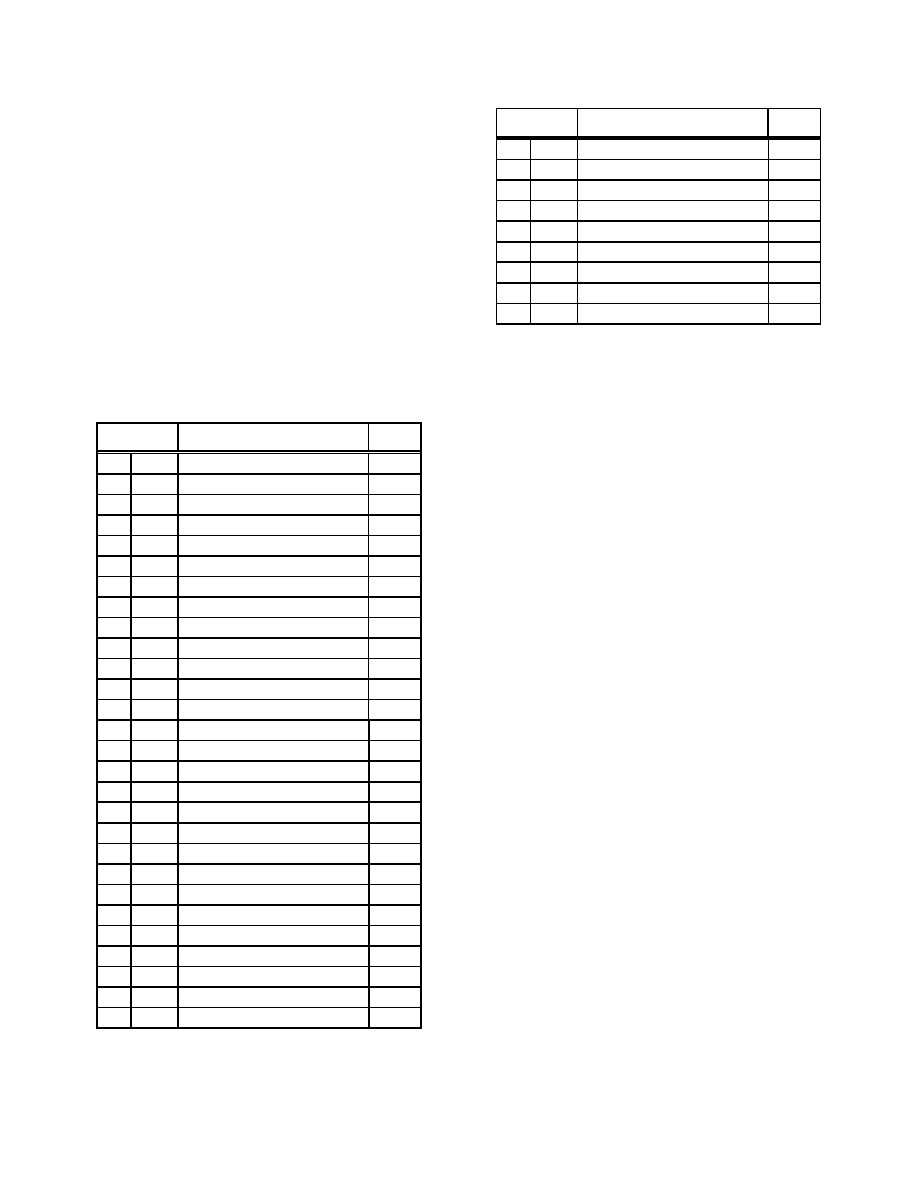
Channel Codec Sub-System
The Channel Codec processes data from two principal sources;
traffic and signaling. The former is normally continuous and
the latter determined on demand. Traffic comes in two forms;
speech and user data. The various traffic sources and the
signaling sources are all processed differently at the physical
layer. Speech traffic data is supplied by the speech transcoder
and the remaining data types are sourced from the Control
Processor and interfaced via a dedicated data interface. The
Channel Codec subsystem functional block diagram is shown
in Figure 3.
DSP
INTERFACE
REGISTERS
DEINTERLEAVE
INTERLEAVE
ENCODE
DECODE
ENCRYPT
DECRYPT
VBC
INTERFACE
TEST
INTERFACE
H8
INTERFACE
RADIO / SYNTHESIZER
TIMING AND CONTROL
Figure 3. Channel Codec Subsystem
The transmit and receive functions of the Channel Codec are
timed by an internal timebase that maintains accurate timing
of all sub-systems. This timebase is aligned with the on-air
receive signal and all system control signals, both internal and
external, are derived from it.
The physical layer processing can be divided into 4 phases,
two each for up- and downlink. The data in the transmit path
undergoes an ENCODE phase and then a TRANSMIT phase.
Similarly, data in the downlink path is termed the receive data
and it undergoes a RECEIVE phase followed by a DECODE
phase. The buffer between the ENCODE and TRANSMIT
functions is the INTERLEAVE module that holds the data and
permits the building of the transmit burst structure. Similarly
the DEINTERLEAVE module forms the buffer between the
RECEIVE and the DECODE processes.
Each of these four phases is controlled explicitly by the
Control Processor via control registers that define the mode of
operation of each sub-module and the data source they should
process. Typically these control values are updated every
TDMA frame in response to interrupts from the internal
timebase.
The ENCODE process involves the incorporation of error
protection codes. All data is sourced in packets and two forms
of error coding applied; block coding (parity or Fire code) and
convolution coding. The resultant data block is then written to
the INTERLEAVE module where it is buffered in a RAM.
Data is read from the interleave buffer memories contiguously
but written in non-contiguous manner, thereby implementing
the interleaving function. The TRANSMIT process uses a
different time structure now associated with the on-air TDMA
structure. The data is read from the INTERLEAVE module
and formatted into bursts with the requisite timing. This
involves adding fixed patterns such as the tail bits and training
sequence code. The resultant burst is written to the external
Baseband Converter where the modulation is performed and
the output timed to the system timebase before transmission.

Preliminary Technical Information
AD6426
This Information applies to a product under development. Its characteristics and specifications are subject to change without notice. Analog Devices assumes no
obligation regarding future manufacture unless otherwise agreed to in writing. No responsibility is assumed by Analog Devices for its use; nor for any
infringements of patents or other rights of third parties which may result from its use. No license is granted by implication or otherwise under any patent or patent
rights of Analog Devices.
Revision Preliminary 2.3 (June 9, ´98)
- 8 -
Confidential Information
A feature of the GSM system is the application, as part of the
TRANSMIT process, of data encryption for the purpose of link
security. After the INTERLEAVE module the data may be
encrypted using the prescribed A5/1 or A5/2 encryption
algorithm.
The RECEIVE function requires unmodulated baseband data
from the equalizer. As necessary the data is decrypted and
written to the DEINTERLEAVE module. This is conducted at
TDMA frame rate, although precise timing is not necessary at
this stage.
The DECODING process reads data from the
DEINTERLEAVE module, inverting the interleave algorithm
and decodes the error control codes, correcting and flagging
errors as appropriate. The data also includes a measure of
confidence expressed as two additional bits per received
symbol. These are used in the convolution decoder to improve
the error decoding performance. The resultant data is then
presented to the original sources as determined by the control
programming. The Channel Codec interfaces with the speech
transcoder for speech traffic data and with an equalizer for
recovered receive data. In the AD6426 the equalizer and
speech transcoder are implemented in the DSP.
Processor Sub-System
The Processor Sub-System consists of a high performance 16-
bit microcontroller together with a selection of peripheral
elements. The processor is a version of the Hitachi H8/300H
that has been developed to support GSM applications and
which is well suited to support the Protocol Stack and
Application Layer software.
DSP Sub-System
The DSP Sub-System consists of a high performance 16-bit
digital signal processor (DSP) with integrated RAM and ROM
memories. The DSP performs two major tasks: speech
transcoding and channel equalization. Additionally several
support functions are performed by the DSP. The instruction
code, which advises the DSP to perform these tasks, is stored
in the internal ROM. The DSP sub-system is completely self-
contained, no external memory or user-programming is
necessary.
Speech Transcoding
In Full Rate mode the DSP receives the speech data stream
from the EVBC and encodes the data from 104 kbit/s to 13
kbit/s. The algorithm used is Regular Pulse Excitation, with
Long Term Prediction (RPE-LTP) as specified in the 06-series
GSM Recommendations.
In Enhanced Full Rate mode, the DSP encodes the 104 kbit/s
speech data into 12.2 kbit/s (speech) +0.8 kbit/s (CRC and
repetition bits) as additionally specified in the Phase 2 version
of the 06-series GSM Recommendations. In both modes, the
DSP also performs the appropriate voice activity detection and
discontinuous transmission (VAD/DTX) functions.
Alternatively the DSP receives encoded speech data from the
channel codec sub-system including the Bad Frame Indicator
(BFI). The Speech decoder supports a Comfort Noise Insertion
(CNI) function that inserts a predefined silence descriptor into
the decoding process. The resulting data, at 104 kbit/s, is
transferred to the EVBC.
Equalization
The Equalizer recovers and demodulates the received signal
and establishes local timing and frequency references for the
mobile terminal as well as RSSI calculation. The equalization
algorithm is a version of the Maximum Likelihood Sequence
Estimation (MLSE) using the Viterbi algorithm. Two
confidence bits per symbol provide additional information
about the accuracy of each decision to the channel codec's
convolutional decoder. The equalizer outputs a sequence of
bits including the confidence bits to the channel codec sub-
system.
Audio Control
The DSP subsystem is also responsible for the control of the
audio path. The EVBC provides two audio inputs and two
audio outputs, as well as a separate buzzer output, which are
switched and controlled by the DSP. Furthermore the EVBC
provides for variable gain and sensitivity which is also
controlled by the DSP under command of the Layer 1
software.
Tone Generation
All alert signals are generated by the DSP and output to the
EVBC. These alerts can be used for the buzzer or for the
earpiece. The tones used for alert signals can be fully defined
by the user by means of a description which provides all the
parameters required such as frequency content and duration of
components of the tone. The tone descriptions are provided by
the Layer 1 software.
Automatic Frequency Control (AFC)
The detection of the frequency correction burst provides the
frequency offset between the mobile terminal and the received
signal. This measure is supplied to the Layer 1 software which
then requests a correction of the master clock oscillator
frequency via the AFC-DAC in the EVBC. In order to do so
the Layer 1 software includes a transfer function for the
oscillator frequency against the voltage applied. The DSP
provides the measurements for the AFC.
Automatic Gain Control (AGC)
The DSP is also responsible for making measurements of the
power in the received signal. This is used for a number of
functions including RSSI measurement, adjacent channel
monitoring and AGC. The Layer 1 software passes the
requested gain level to the DSP, which then analyzes the
received signal and generates an AGC control signal.
Depending on the radio architecture, this control signal will be
used in digital form or, converted by the AD6425 in analog
form.
Preliminary Technical Information
AD6426
This Information applies to a product under development. Its characteristics and specifications are subject to change without notice. Analog Devices assumes no
obligation regarding future manufacture unless otherwise agreed to in writing. No responsibility is assumed by Analog Devices for its use; nor for any
infringements of patents or other rights of third parties which may result from its use. No license is granted by implication or otherwise under any patent or patent
rights of Analog Devices.
Revision Preliminary 2.3 (June 9, ´98)
- 9 -
Confidential Information
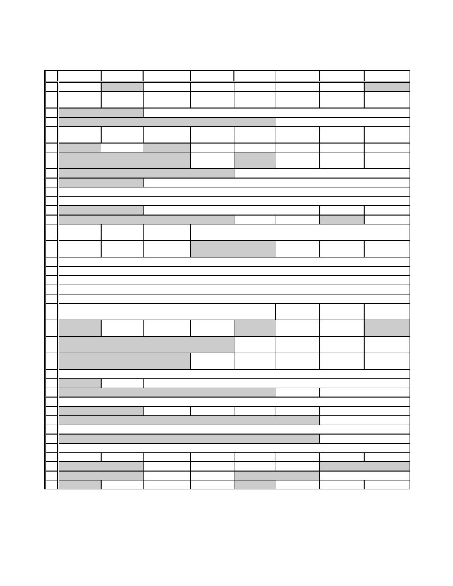
REGISTERS
The AD6426 contains 88 Channel Codec Control Registers, 69
H8 Peripheral Registers mapped into the Channel Codec
address space starting at 8000h. All registers are normally
accessed by the Layer 1 software provided with the
AD20msp425 chipset. The user is not expected to read or
write to any registers other than through the Layer 1 software.
Therefore only a limited description of these registers is given
here to ease the understanding of the functional behavior of
the AD6426. Only registers which can be modified or
monitored by the user under control of the Layer 1 software
are shown. The Channel Codec Control Registers are listed in
Table 1, and the H8 Peripheral Control Registers in Table 3
A description of the Channel Codec Control Register contents
is shown in Table 2, and of the H8 Peripheral Registers in
Table 4.
Table 1. CC Control Registers
Address
Name
0
00 H
SYSTEM
R/W
2
02 H
RADIO CONTROL
R/W
4
04 H
BSIC
R/W
5
05 H
TSC
R/W
6
06 H
TRAFFIC MODE
R/W
7
07 H
DAI
R/W
8
08 H
EEPROM
R/W
9
09 H
KEYPAD COLUMN
R/W
10
0A H
KEYPAD ROW
RD
28
1C H
EVBC SERIAL 1
RMW
29
1D H
EVBC SERIAL 2
RMW
30
1E H
EVBC IF CONTROL
R/W
35
23 H
RESET
R/W
37
25 H
SYNTH BIT COUNT
R/W
38
26 H
SYNTH CONTROL
R/W
39
27 H
ERROR COUNT
RMW
40
28 H
SYNTHESIZER 1
WR
41
29 H
SYNTHESIZER 2
WR
42
2A H
SYNTHESIZER 3
WR
43
2B H
SYNTHESIZER 4
WR
44
2C H
POWER CONTROL INT
R/W
45
2D H
POWER CONTROL EXTERNAL
R/W
46
2E H
SWRESET 1
R/W
47
2F H
SWRESET 2
R/W
48
30 H
INTERRUPT COUNTER
R/W
49
31 H
BBC TX ADDRESS
R/W
50
32 H
BACKLIGHT
WR
51
33 H
VERSION CONTROL
RD
Address
Name
72
48 H
SYNTHESIZER PROGRAM
R/W
73
49 H
TXPA OFFSET 1
R/W
74
4A H
TXPA OFFSET 2
R/W
75
4B H
TXPA WIDTH 1
R/W
76
4C H
TXPA WIDTH 2
R/W
77
4D H
IRQ ENABLE
R/W
78
4E H
IRQ LATCH
RMW
79
4F H
CC GPIO
R/W
88
58 H
ccGPO
R/W
Preliminary Technical Information
AD6426
This Information applies to a product under development. Its characteristics and specifications are subject to change without notice. Analog Devices assumes no
obligation regarding future manufacture unless otherwise agreed to in writing. No responsibility is assumed by Analog Devices for its use; nor for any
infringements of patents or other rights of third parties which may result from its use. No license is granted by implication or otherwise under any patent or patent
rights of Analog Devices.
Revision Preliminary 2.3 (June 9, ´98)
- 10 -
Confidential Information
Table 2. CC Control Register Contents
#
7
6
5
4
3
2
1
0
0
Autocalibrate
Backlight 1
Test Data Enable Calibrate Radio
Encryption Type
Encrypt Key Load
2
Tx Monitor
Enable
Tx Phase
Polarity
Rx Radio Control
Polarity
Tx Radio Control
Polarity
Tx PHASE
Enable
Monitor
Enable
Receive
Enable
Transmit
Enable
4
Base Station Identity Code
5
Training Sequence Code
6
TxPA
Polarity
INT COUNT[8]
OCE OVERRIDE
Interrupt Counter
Override
Autocalibration
Type
Traffic Frame
Enable
Decryption
Enable
Encryption
Enable
7
BAND ENABLE
NMI Select
GPO10 Data
GPO10 Select
Data Ser. Select
DAIRESET
8
EEPROM Data
Output Enable
EERPOM
Clock
EEPROM
Enable
EERPOM
Data
9
Keypad Column
10
Keypad Row
28
EVBC Serial Port ( 15 : 8 )
29
EVBC Serial Port ( 7 : 0 )
30
Tx Data Delay
EVBC Rx-Buff. full EVBC Tx-Buf.empty
35
EVBC Reset
DSP Reset
CC Reset
37
Isolate
Synthesizer
Config. Dynam.
Synthesizer
Synthesizer
Interface active
Synthesizer Bit Count
38
Synthesizer
Enable Polarity
Synthesizer
Enable Type
Synthesizer
Clock Polarity
Synthesizer
Load Dynamic 1
Synthesizer
Load Dynamic 2
Synthesizer
Clock
39
Error Count
40
Synthesizer (31: 24)
41
Synthesizer (23: 16)
42
Synthesizer (15: 8)
43
Synthesizer (7: 0)
44
Backlight Duty Cycle
Synth. Interface
Power Enable
DSP Interface
Power Enable
Encryption Power
Enable
45
Coprocessor
Power Control
Output Clock
Enable
GP Power
Control
DSP Power
Control
Radio Power
Control
46
Encryption
SW-Reset
EVBC Interface
SW-Reset
DSP Interface
SW-Reset
Synthes. Interface
SW-Reset
47
INT CNT RST
Decode
SW-Reset
Deinterleave
SW-Reset
interleave
SW-Reset
Encode
SW-Reset
48
Interrupt Counter
49
EVBC Read
EVBC Tx Address
50
Modulate 1
Backlight LED Control
51
Version
72
Disable Synth.1
Disable Synth. 0 Synt. Enable Sel.
Synt. Mode
Pin Mode
73
TD ( 9 : 8 )
74
TD ( 7 : 0 )
75
TW ( 9 : 8 )
76
TW ( 7 : 0 )
77
GPO11 Data
GPO11 Select
IRQ5 Enable
IRQ4 Enable
IRQ3 Enable
IRQ2 Enable
FLASHPWD dis.
NMI Edge Pol.
78
IRQ5 active
IRQ4 active
IRQ3 active
IRQ2 active
79
GPIO9 OP En
GPIO8 OP En
GPIO9 Data
GPIO8 Data
88
GPO19 Sel
GPO18 Sel
GPO17 Sel
GPO19
GPO18
GPO17
Preliminary Technical Information
AD6426
This Information applies to a product under development. Its characteristics and specifications are subject to change without notice. Analog Devices assumes no
obligation regarding future manufacture unless otherwise agreed to in writing. No responsibility is assumed by Analog Devices for its use; nor for any
infringements of patents or other rights of third parties which may result from its use. No license is granted by implication or otherwise under any patent or patent
rights of Analog Devices.
Revision Preliminary 2.3 (June 9, ´98)
- 11 -
Confidential Information
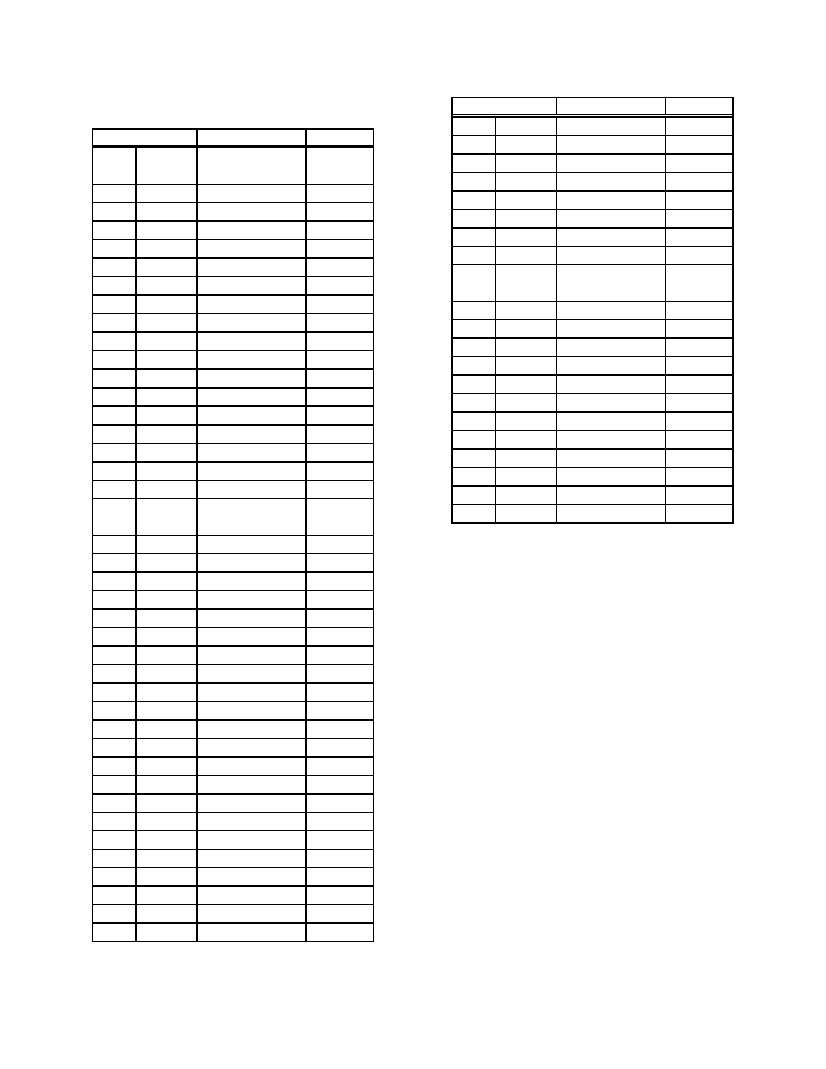
Table 3. H8 Peripheral Control Registers
Address
Name
0
8000h
SMSMR
R/W
1
8001h
SMBRR
R/W
2
8002h
SMSCR
R/W
3
8003h
SMDR
W
4
8004h
SMSSR
R/W
5
8005h
SMDR
R
6
8006h
SMSCMR
R/W
10
8010h
BUFRBR
R
10
8010h
BUFTHR
W
10
8010h
BUFDLL
R/W
11
8011h
BUFIER
R/W
11
8011h
BUFDLM
R/W
12
8012h
BUFIIR
R
12
8012h
BUFFCR
W
13
8013h
BUFLCR
R/W
14
8014h
BUFMCR
R/W
15
8015h
BUFLSR
R/W
16
8016h
BUFMSR
R/W
17
8017h
BUFSCR
R/W
18
8018h
UIBRBR
R
18
8018h
UIBTHR
W
19
8019H
UIBSSR
R/W
26
801AH
UIBER
R
27
801BH
UIBTSR
R
28
801CH
UIBTLR
R/W
29
801Dh
UIBBLR
R
32
8020h
FIXRBR
R
32
8020h
FIXTHR
W
32
8020h
FIXDLL
R/W
33
8021h
FIXIER
R/W
33
8021h
FIXDLM
R/W
34
8022h
FIXIIR
R
35
8023h
FIXLCR
R/W
36
8024h
FIXMCR
R/W
37
8025h
FIXLSR
R/W
38
8026h
FIXMSR
R/W
39
8027h
FIXSCR
R/W
48
8030h
SCCR
R/W
49
8031h
SPSSR
R/W
50
8032h
SDIR1 (MS)
R
51
8033h
SDIR0 (LS)
R
52
8034h
SDOR1 (MS)
W
53
8035h
SDOR0 (LS)
W
Address
Name
64/65
8040/1h
DISPDDR
W
66
8042h
DISPCR
R/W
67
8043h
DDOR
W
68
8044h
DDIR
R
69
8045h
DRR
R/W
72
8048h
WDTR
W
80
8050h
MEM IF
R/W
81
8051h
PERST
R/W
82
8052h
PERCR
R/W
84
8054h
TAR
R/W
85
8055h
PERCLK
R/W
96
8060h
RTCTR1
R/W
97
8061h
RTCTR2
R/W
98
8062h
RTCTR3
R/W
99
8063h
RTCTR4
R/W
100
8064h
RTCTR5
R/W
101
8065h
RTCAR1
R/W
102
8066h
RTCAR2
R/W
103
8067h
RTCAR3
R/W
104
8068h
RTCCR
R/W
105
8069h
RTCSRZ
R/W
106
8074h
SERDISPLAY/NMI
R/W
Preliminary Technical Information
AD6426
This Information applies to a product under development. Its characteristics and specifications are subject to change without notice. Analog Devices assumes no
obligation regarding future manufacture unless otherwise agreed to in writing. No responsibility is assumed by Analog Devices for its use; nor for any
infringements of patents or other rights of third parties which may result from its use. No license is granted by implication or otherwise under any patent or patent
rights of Analog Devices.
Revision Preliminary 2.3 (June 9, ´98)
- 12 -
Confidential Information
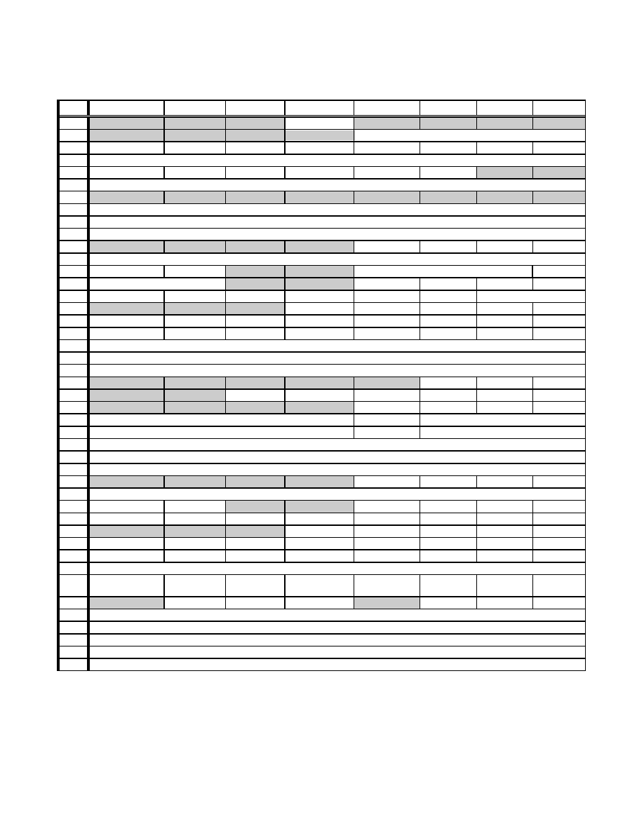
Table 4. H8 Peripheral Register Contents
#
7
6
5
4
3
2
1
0
0
ODD
1
BRR[3:0]
2
TIE
RIE
TE
RE
AE
DATEN
CLKPOL
CLKEN
3
Transmit[7:0]
4
TDRE
RDRF
ORER
ERS
PER
TEND
5
Receive[7:0]
6
10
RxData[7:0]
10
TxData[7:0]
10
BRR[7:0]
11
EDSSI
ELSI
ETBEI
ERBFI
11
BRR[15:8]
12
FIFO ST
FIFO ST
InterruptID[2:0]
Int Pend
12
RxLevel[1:0]
DMA
TX FIFO
RX FIFO
FIFO EN
13
DLAB
SET BRK
Stick Par.
Ev. Parity
Parity EN
Stop Bits
WLS[1:0]
14
Loop
Out2
Out1
RTS
DTR
15
Error Rx FIFO
TEMT
THRE
Break Interrupt
Framing Error
Parity Error
Overrun Error
Data Ready
16
DCD
RI
DSR
CTS
DDCD
TERI
DDSR
DCTS
17
SCR[7:0]
18
RxData[7:0]
18
TxData[7:0]
19
MRESET
UIB Enable
PROC
26
TE
RE
FE
PE
BI
OE
27
MODEM
TX Level
RX Time
RX Level
28
Tx Trigger Level [3:0]
Rx Trigger Level [3:0]
29
Chars in TX Buffer [3:0]
Chars in Rx Buffer [3:0]
32
RxData[7:0]
32
TxData[7:0]
32
BRR[7:0]
33
EDSSI
ELSI
ETBEI
ERBFI
33
BRR[15:8]
34
FIFO ST
FIFO ST
InterruptID[2:0]
Int Pend
R
35
DLAB
SET BRK
Stick Par.
Ev. Parity
Parity EN
Stop Bits
WLS[1:0]
R/W
36
Loop
Out2
Out1
RTS
DTR
37
Error Rx FIFO
TEMT
THRE
Break Interrupt
Framing Error
Parity Error
Overrun Error
Data Ready
38
DCD
RI
DSR
CTS
DDCD
TERI
DDSR
DCTS
39
SCR[7:0]
48
TEST
RX MODE
CLOCK
TX ENABLE
CROSSPOINT
SWITCH
UCONN
SWITCH
R/W
49
SDORIE
SDIROE IE
SDIRIE
SDOR EMT
SDIR OE
SDIR FULL
50
Receive[15:8]
51
Receive[7:0]
52
Transmit[15:8]
53
Transmit[7:0]
64/65
Data[7:0]
Preliminary Technical Information
AD6426
This Information applies to a product under development. Its characteristics and specifications are subject to change without notice. Analog Devices assumes no
obligation regarding future manufacture unless otherwise agreed to in writing. No responsibility is assumed by Analog Devices for its use; nor for any
infringements of patents or other rights of third parties which may result from its use. No license is granted by implication or otherwise under any patent or patent
rights of Analog Devices.
Revision Preliminary 2.3 (June 9, ´98)
- 13 -
Confidential Information
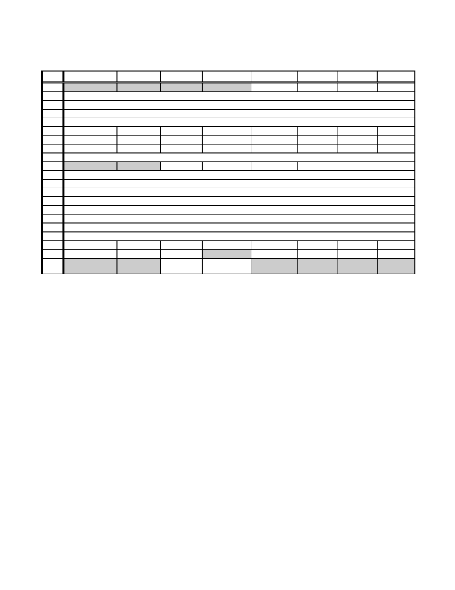
H8 Peripheral Register Contents (Continued)
#
7
6
5
4
3
2
1
0
66
SDISP POL
DISP CLKEN
CLK FREQ
DDREMT
67
Transmit Data [7:0]
68
Receive Data [7:0]
69
Reset Data [7:0]
72
WDT[7:0]
80
TEST CLK
Unused
Unused
UART SEL
DALLAS EN
RAM SEL7
DISP
SRAM16
81
WDT INT
RTC INT
KEYINT
DALLAS INT
FA INT
UA INT
SSINT
MONINT
82
WDT IE
RTC IE
KEY IE
DALLAS IE
FA IE
UA IE
SS IE
MONIE
84
Test Key[7:0]
85
USCCLK EN
BUCLK EN
FUCLK EN
DSPPLL[2:0]
96
TR[1]
97
TR[2]
98
TR[3]
99
TR[4]
100
TR[5]
101
AR[1]
102
AR[2]
103
AR[3]
104
INTEN
TIMWEN
ALAWEN
PWRUEN
AGCENN
FBENN
Unused
Unused
105
INT
TIMER
ALARM
APWRUP
OSCFAIL
32K PRESENT
TESTOUT
106
TXENABLE
NMI
SERDISP MODE
Preliminary Technical Information
AD6426
This Information applies to a product under development. Its characteristics and specifications are subject to change without notice. Analog Devices assumes no
obligation regarding future manufacture unless otherwise agreed to in writing. No responsibility is assumed by Analog Devices for its use; nor for any
infringements of patents or other rights of third parties which may result from its use. No license is granted by implication or otherwise under any patent or patent
rights of Analog Devices.
Revision Preliminary 2.3 (June 9, ´98)
- 14 -
Confidential Information
GENERAL CONTROL
Clocks
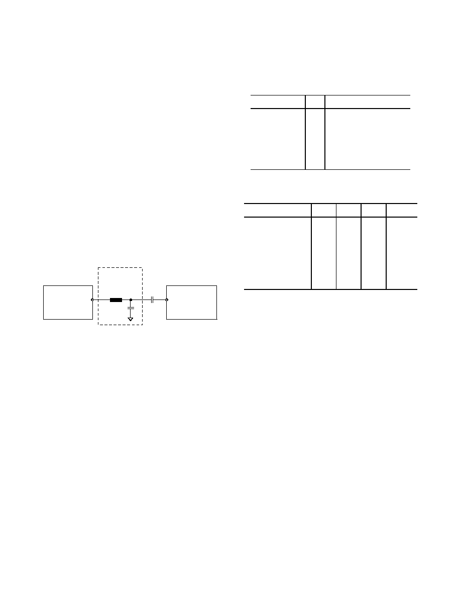
Clock Input
The AD6426 requires a single 13 MHz, low level clock signal,
which has to be provided at the pin CLKIN. For proper
operation a signal level of 250 mV
PP
minimum is required.
This feature eases system design and reduces the need for
external clock buffering. Only minimal external components
are required as shown in Figure 4.
The internal clock buffer can accept any regular waveform as
long as it can find voltage points in the signal, for which a
50% duty cycle can be determined. This condition is met for
sinewaves, triangles, or slew-limited square waves. Dedicated
circuitry searches for these points and generates the respective
bias voltage internally.
The external capacitor (1nF) decouples the bias voltage of the
clock signal generated by the oscillator from the internally
generated bias voltage of the clock buffer circuitry.
The LC-filter shown is optional. It ensures, that the input
signal is "well behaved" and sinusoidal. Additionally it filters
out harmonics and noise, that may be on top of the pure 13
MHz signal.
13 MHz
VCTCXO
AD6422
OUT
CLKIN
1nF
2.2
µ
H
68 pF
Optional
13 MHz Filter
Figure 4. Clock Input Circuitry
Clock Output
The input clock drives both the H8 and the Channel Codec
directly. A gated version, controlled by the Output Clock
Enable flag in CC Control Register 45, drives the CLKOUT
pin of the EVBC interface. The stand-by state of CLKOUT is
logic zero. The CLKOUT output will be active on reset.
Slow Clocking
To reduce power consumption of AD20msp425 solutions, a
new slow clocking scheme has been designed into the
AD6426. This scheme allows the VCTCXO to be powered
down between paging blocks during Idle Mode and for a
32.768kHz oscillator to keep the time reference during this
period. Only a common 32.768kHz watch crystal is required to
take advantage of this scheme. As in previous generations,
power consumption is also kept to a minimum using
asynchronous design techniques and by stopping all
unnecessary clocks.
Layer 1 software and logic built into the AD6426 are
responsible for maintaining synchronization and calibration of
the slow clock and ensure the validity of the time reference
under all circumstances. The active-high OSC13MON output
is prevented from becoming inactive if the 32.768kHz signal is
not present. The following table describes the functionality of
the relevant pins.
Name
I/O
Function
OSCIN
I
32.768kHz Crystal Input
OSCOUT
O
32.768kHz Oscillator
Output
OSC13MON
O
13 MHz Oscillator Power
Control
PWRON
O
Power ON/OFF Control
The following table lists the recommended specification for a
32kHz crystal.
Parameter
Min
Typ
Max
Units
ESR
50
k
Shunt Capacitance
2
pF
Load Capacitance
6
12.5
30
pF
Turnover
Temperature (T
o
)
25
°C
Parabolic Curvature
Constant (K)
0.040
ppm/°C
Real Time Clock and Alarm
The AD6426 provides a simple Real Time Clock (RTC) using
the 32.768kHz clock input. A 40 bit counter allows for more
than one year of resolution. The RTC module contains a
32.768kHz on chip oscillator buffer designed for very low
power consumption and a set of registers for a timer, alarm,
control and status functions.
The RTC circuit is supplied by two sources; a VDDRTC
supply pin and the main system VDD. It is the handset
designer's responsibility to provide suitable switching
between the main system VDD and a backup supply to ensure
the RTC module is permanently powered.
The VDDRTC pin is intended to interface to a backup battery
circuit or charge holding network in order for the RTC to
maintain timing accuracy when the main battery is removed
and the handset is powered down.
The user can set an alarm time at which the handset powers
up. If an alarm time is set, the current time matches the alarm
time, and the power on alarm feature is enabled, the handset is
powered up by asserting the PWRON pin for a period of
approximately 2 seconds.
Preliminary Technical Information
AD6426
This Information applies to a product under development. Its characteristics and specifications are subject to change without notice. Analog Devices assumes no
obligation regarding future manufacture unless otherwise agreed to in writing. No responsibility is assumed by Analog Devices for its use; nor for any
infringements of patents or other rights of third parties which may result from its use. No license is granted by implication or otherwise under any patent or patent
rights of Analog Devices.
Revision Preliminary 2.3 (June 9, ´98)
- 15 -
Confidential Information
The VDDRTC was designed to interface with either a:
·
Lithium Battery or
·
Capacitor in the range of 0.4F (maximum for ~24 hours
standby) to 8mF (~30 minutes standby)
Reset
The AD6426 is reset by setting the RESET pin to GND. This
will reset the H8-processor, the Channel Codec, the internal
DSP as well as the LCD controller interface and Boot ROM
logic. Both the DSP and the Channel Codec will be held in
reset until the RESET register is written to by the H8. At least
50 CLKIN cycles must elapse before deasserting the RESET
pin and at least a further 100 cycles before writing to the
RESET register.
For reset at power up, the DSP must be held in reset for at
least 2000 clock cycles to enable the internal PLL to lock.
The RESET CC Control Register 35 contains the following
flags:
Bit
Function
3
EVBC Reset
2
DSP Reset
0
Channel Codec Reset
Additionally 8 functional modules can be reset under control
of the two SWRESET registers:
Bit
SWRESET 1 CC Control Register 46
3
Encryption Software Reset
2
EVBC Interface Software Reset
1
DSP Interface Software Reset
0
Synthesizer Interface Software Reset
Bit
SWRESET 2 CC Control Register 47
3
Decode Software Reset
2
Deinterleave Software Reset
1
Interleave Software Reset
0
Encode Software Reset
The JTAG circuitry is reset by a power-on reset mechanism.
Further resets must be done by asserting the TMS input high
for at least five TCK clock cycles. When JTAG compliance is
re-enabled, the JTAG is reset forcing the AD6426 into its
normal mode of operation, selecting the BYPASS register by
default.
The H8 fetches its program start vector from location 0x0000
in segment zero. This can either be from external ROM or
internal Boot ROM, depending on the status of the
BOOTCODE pin.
Interrupts
The interrupts are controlled by the two CC Control Registers
77 and 78. These registers only apply to Emulation Mode, in
that they define which of the interrupts are able to assert
CCIRQ2.
Bit
IRQ ENABLE CC Control Register 77
5
IRQ 5 Enable
4
IRQ 4 Enable
3
IRQ 3 Enable
2
IRQ 2 Enable
Bit
IRQ LATCH CC Control Register 78
5
IRQ 5 active
4
IRQ 4 active
3
IRQ 3 active
2
IRQ 2 active
NMI
The non-maskable interrupt NMI input of the H8 processor is
multiplexed with the IRQ6 pin. IRQ6 is the default function,
though asserting the NMI Select flag in CC Control Register 7
will select the NMI function. When not selected, NMI will be
tied off high internally, though it remains driven by the JTAG
port for test purposes. The signal is programmable to be edge
or level sensitive. It defaults to falling edge. The edge polarity
can be changed by programming the H8. However, if
FLASHPWD is used then the same setting must be applied to
CC Control Register 77. The default of zero implies falling
edge sensitive. This way NMI going active can correctly de-
assert FLASHPWD. The NMI can be used for test purposes or
user defined features. NMI is capable of bringing the control
processor out of software standby mode and therefore suitable
for functions such as alarm inputs, power management etc.
During manufacture the NMI can be used to trigger special
test code.
In addition NMI can be generated internally thus freeing up
the IRQ6 PIN. In this mode the TXENABLE NMI will occur
on the rising edge of the TXENABLE as seen at the pin. The
H8 should be set up for a negative edge NMI in this case.
Setting bit 5 in the SERDISPLAY/NMI H8 Peripheral Control
Register 106 to a ONE enables the TXENABLE NMI.
However, the Layer 1 Software must program the external INT
pin to INT6 before the register bit is set.
Preliminary Technical Information
AD6426
This Information applies to a product under development. Its characteristics and specifications are subject to change without notice. Analog Devices assumes no
obligation regarding future manufacture unless otherwise agreed to in writing. No responsibility is assumed by Analog Devices for its use; nor for any
infringements of patents or other rights of third parties which may result from its use. No license is granted by implication or otherwise under any patent or patent
rights of Analog Devices.
Revision Preliminary 2.3 (June 9, ´98)
- 16 -
Confidential Information
Wait
The H8 microprocessor WAIT input signal can be controlled
externally by programming the FLASHPWD pin to switch to
the WAIT input function. Setting the flag FLASHPWD Disable
in CC Control Register 77 to 1 and GPO11 Select to 0,
transforms the FLASHPWD output pin into a WAIT input pin.
External devices driving WAIT must drive high on reset and
until the software has changed the FLASHPWD pin to the
WAIT function.
Automatic Booting
To allow download of FLASH memory code into the final
system, the AD6426 provides a small dedicated routine to
transfer code through the Data Interface into the FLASH
memory. This routine is activated by asserting the
BOOTCODE pin.
Power Control
The AD6426 and Layer 1 software is optimized to minimize
the mobile radio power consumption in all modes of operation.
Two power control registers are dedicated for activating and
deactivating functional modules:
Bit
POWER CONTROL INTERNAL CC Control
Register 44
2
Synthesizer Interface Power Enable
1
DSP Interface Power Enable
0
Encryption Power Enable
Bit
POWER CONTROL EXTERNAL CC Control
Register 45
5
Output Clock Enable (will reset to 1)
4
General Purpose Power Control
2
DSP Power Control
1
Radio Power Control
INTERFACES
The GSM Processor provides eleven external interfaces for
dedicated purposes:
1. Memory Interface
2. EEPROM Interface
3. SIM Interface
4. Accessory Interface
5. Universal System Connector Interface
6. Keypad / Backlight / Display Interface
7. Battery ID Interface
8. Voiceband/Baseband Converter (EVBC)
Interface
9. Radio Interface
10. Test Interface
11. Debug Interface
Memory Interface
The memory interface of the AD6426 serves two purposes.
Primarily, it provides the data, address, and control lines for
the external memories (RAM and ROM / FLASH Memory).
Secondly, the data and address lines are used to interface with
the display. The pins of the memory interface are listed in
Table 5.
Table 5. Memory Interface
Name
I/O
Function
ADD20 : 0
O
Address bus
DATA15:0
I/O
Data bus
RD
O
Read strobe
HWR
O
High write strobe / Upper
Byte Strobe
LWR
O
Low write strobe / Lower
Byte Strobe
WR
O
Write Strobe
RAMCS
O
RAM chip select
ROMCS
O
FLASH / ROM chip select
FLASHPWD
O
FLASH Powerdown
The HWR and LWR pins can be configured to function as
UBS and LBS, respectively, by setting the SRAM16 bit (bit 0)
of the MEMIF H8 Peripheral Control Register 80. This bit is
reset at power-up. When configured as UBS and LBS, these
pins facilitate access of 16-bit SRAM in conjunction with the
Read/Write Strobes.
The pin FLASHPWD is automatically asserted low when the
H8 enters the Software Standby Mode, and de-asserted when
an interrupt causes the H8 to exit the Software Standby Mode.
This allows the use of "deep power down mode" for certain
FLASH memories. Also the entire data bus is driven low
during software standby mode.
EEPROM Interface
The AD6426 provides a 3-wire interface to an external
EEPROM by using three GPIOs of the control processor.
Table 6 shows the functionality of these three pins.
Table 6. EEPROM Interface
Name
I/O
Function
EEPROMDATA
I/O
EEPROM data
EEPROMCLK
O
EEPROM clock
EEPROMEN
O
EEPROM enable
Preliminary Technical Information
AD6426
This Information applies to a product under development. Its characteristics and specifications are subject to change without notice. Analog Devices assumes no
obligation regarding future manufacture unless otherwise agreed to in writing. No responsibility is assumed by Analog Devices for its use; nor for any
infringements of patents or other rights of third parties which may result from its use. No license is granted by implication or otherwise under any patent or patent
rights of Analog Devices.
Revision Preliminary 2.3 (June 9, ´98)
- 17 -
Confidential Information
The EEPROM interface is controlled entirely through software
via the EEPROM register. This allows support for every
desired timing and protocol.
Bit
EEPROM CC Control Register 8
4
EEPROM Data Output Enable
when set to 1, the content of bit 0 will be written to
the pin.
2
EEPROM Clock
Connected to the EEPROMCLK pin
1
EEPROM Enable
Connected to the EEPROMENABLE pin
0
EEPROM Data
Connected to the EEPROMDATA pin
SIM Interface
The AD6426 allows direct interfacing to the SIM card via a
dedicated SIM interface. This interface consists of 7 pins as
shown in Table 7. Some applications may not require
SIMPROG and SIMCARD; thus SIMPROG and SIMCARD
can be re-used as additional general purpose I/O-pins.
Table 7. SIM Interface
Name
I/O
Function
SIMCARD
I
SIM card detect
SIMDATAOP
O
SIM data output
SIMDATAIP
I
SIM data input
SIMCLK
O
SIM clock
SIMRESET
O
SIM reset
SIMPROG
O
SIM program enable
SIMSUPPLY
O
SIM supply enable
Accessory Interface
The AD6426 provides 12 interface pins listed in Table 8 for
control of peripheral devices such as a car kit. However, two
general purpose I/O-pins of the Accessory Interface are
proposed to be used for additional control of the radio section
as described in the Radio Interface chapter.
Table 8. Accessory Interface
Name
I/O
Function
GPIO9:0
I/O
General purpose
inputs/outputs
GPCS
O
General purpose chip select
All GPIO pins start up as inputs. GPIO8 and GPIO9 are
controlled by flags in CC Control Register 79. When the
GPIOn OP Enable flag is set to 0, the GPIOn Data flag
reflects the input pin state when read and writing to GPIOn
Data has no effect.
When the GPIOn OP Enable flag is set to 1, the GPIOn Data
flag returns when read the last value written to it and controls
the GPIOn pin when written to it.
Additional general purpose inputs and outputs are available
under software control. The following pins shown in Table 9
become general purpose inputs/outputs or outputs.
Table 9. Additional GPIO / GPO Pins
Pin Name
I/O
New Function
SIMCARD
I/O
GPIO16
SIMPROG
I/O
GPIO15
ADD20
O
GPO10
FLASHPWD
O
GPO11
TXPA
O
GPO12
CALIBRATERADIO
O
GPO13
TXENABLE
O
GPO14
SYNTHEN1
O
GPO17
AGCA
O
GPO18
AGCB
O
GPO19
USCRI
O
GPO20
USCRTS
O
GPO21
USCCTS
I
GPI22
If the pins SIMCARD and SIMPROG are not required in the
application, they can be used as additional H8 programmable
general purpose inputs or outputs.
Setting GPO10 Select (CC Control Register 7) to 1, will
transform the pin ADD20 into a general purpose output
allowing the pin to be directly controlled via GPO10 Data.
By setting GPO11 Select (CC Control Register 77) to 1 and
FLASHPWD Disable to 1, the pin FLASHPWD becomes a
general purpose output. The pin state is toggled by setting the
GPO11 Data flag.
To increase the flexibility of the AD6426, three pins in the
Radio Interface are multiplexed within GPO functions. The
pins multiplexed are: SYNTHEN1, AGCA and AGCB, with
the default function being the Radio Interface. The mode of
these pins is controlled by the Channel Codec Register
ccGPO.
The GPO[n]Sel bit selects the function of the pin. Setting
GPO[n]Sel to one will enable the pin to be controlled by the
GPO[n] bit. The GPO[n]Sel bit will override any other pin
function selection.

Preliminary Technical Information
AD6426
This Information applies to a product under development. Its characteristics and specifications are subject to change without notice. Analog Devices assumes no
obligation regarding future manufacture unless otherwise agreed to in writing. No responsibility is assumed by Analog Devices for its use; nor for any
infringements of patents or other rights of third parties which may result from its use. No license is granted by implication or otherwise under any patent or patent
rights of Analog Devices.
Revision Preliminary 2.3 (June 9, ´98)
- 18 -
Confidential Information
To transform the TXPA pin into a general purpose output, set
TXPA Width = 0 (CC Control Register 75 and 76), then use
TxPA Polarity flag (CC Control Register 6) to toggle pin state.
To use the CALIBRATERADIO pin as a general purpose
output, set the AUTOCALIBRATE flag to zero and use the
CALIBRATERADIO flag to toggle pin state.
Universal System Connector Interface
A typical GSM handset requires multiple serial connections to
provide data during normal phone operation, manufacturing,
testing, and debug. In an ideal case many of these functions
could be combined into a single multi-purpose system
connector. For example, the USC port can be used for:
·
Flash code download for manufacturing and updates
·
Booting - UART interface used to download programs to
H8 memory
·
DAI Acoustic mode testing - connects System Simulator
(SS) directly to EVBC
·
DAI Transcoding mode - connects SS to 6426 for speech
codec testing
·
External DTA (Data Terminal Adapter) - asynchronous
link for MSDI interface
·
RS232 port - for on-board data services
·
H8 debug / monitor
·
Hands-free operation - time shared VBC and H8 port
·
Receive I/Q monitoring
The Universal System Connector (USC) of the 6426 is
designed such that no external glue logic is required to achieve
this multi-purpose functionality. Furthermore, since the USC's
function is related to the voiceband and I/Q data serial ports,
the USC block is also responsible for the correct configuration
of these serial data streams.
The actual system connector has the minimum number of pins
to achieve the needed functionality. This save system pins, and
allows for a more reliable connector from a manufacturing and
mechanical standpoint. The USC defines a 5 pin connector
that multiplexes asynchronous, synchronous, and modem
control signals as needed:
Name
I/O
Function
USCRX
I
Receive Data
USCTX
O
Transmit Data
USCRTS
O
Ready to Send
USCCTS
I/O
Clear to Send / Transmit Frame Sync
USCRI
1/O
Ring Indicator / Serial Clock
Operating modes of the USC
Buffered UART Mode (Booting/Data Services)
This mode attaches the H8/DSP buffered UART to the USC,
bringing out either the serial bit rate clock or the Modem
Control Signal RI. This is the default mode when the phone is
powered up.
The BOOTCODE pin will be latched on RESET high. If
BOOTCODE is high at RESET, execution begins from the
Boot ROM which will configure the buffered UART to
download the FLASH programming code into RAM. The
FLASH program itself is also downloaded via the UART.
An external Data Terminal Adapter can also be used. In this
case Data Services are done external to the phone and then
transferred to and from the H8. With the external Data
Terminal Adapter, the serial bit rate clock output is selected
for USCRI pin.
This mode can be used for a variety of H8 debug tasks as the
UART can be used to simply shift debug information out.
Note that when in this mode if the handshake signals and
serial bit clock are not required, the RTS and RI pins can be
used as extra GPO, and the CTS pin used as an extra GPI.
Time-shared Mode (Multi-switch)
This mode allows time multiplexed communication with both
the H8 and DSP. This is most useful as a hands-free solution,
but can be used for other purposes also e.g., DAI Transcoding
Testing. This mode is used for DAI testing of the DSP's
speech transcoder in which the DSP's SPORT0 is connected to
the USC through the Multi-switch.
DAI Acoustic Mode Testing
This mode is used for DAI testing of the 6425's phone's
acoustic properties. The VSPORT of the 6425 connects to the
USC through the Multi-switch.
IQ Monitoring
This mode is used for testing the RF receive path and allows
access to the I and Q samples from the AD6425. The AD6425
signals are simply routed to the USC. This means that the
clock and frame sync are provided by the 6425 as well.
16 bit Mode
This mode connects the synchronous data path to the
SDIR/SDOR H8 Peripheral Control Registers, giving the H8
full access to the synchronous port bandwidth. This allows a
fast synchronous communication to an external device, and is
intended to be used for a fast download mechanism.
Preliminary Technical Information
AD6426
This Information applies to a product under development. Its characteristics and specifications are subject to change without notice. Analog Devices assumes no
obligation regarding future manufacture unless otherwise agreed to in writing. No responsibility is assumed by Analog Devices for its use; nor for any
infringements of patents or other rights of third parties which may result from its use. No license is granted by implication or otherwise under any patent or patent
rights of Analog Devices.
Revision Preliminary 2.3 (June 9, ´98)
- 19 -
Confidential Information
Keypad / Backlight / Display Interface
This interface combines all functions of display and keyboard
as shown in Table 10.
Table 10. Keypad / Backlight / Display Interface
Name
I/O
Function
KEYPADROW5 : 0
I
Keypad row inputs
KEYPADCOL3 : 0
O
Keypad column strobes
BACKLIGHT
O
Backlight control
DISPLAYCS
O
Display Controller chip
select
LCDCTL
O
LCD Control / Serial Display
Data Output
GPIO3
O
Serial Display Data Output
GPIO4
O
Serial Display Clock Output
By providing 4 keypad-column outputs (open drain, pull low)
and 6 keypad-row inputs the AD6426 can monitor up to 24
keys. Additionally, an extra column can be implemented by
using the "ghost column" method for a total of 30 keys. The
H8 processor is interrupted whenever a key is pressed. The
KEYPADCOL pins are connected to the Keypad Column3-0
flags in the KEYPAD COLUMN CC Control Register 9.
Bit
KEYPAD COLUMN CC Control Register 9
3 : 0
Keypad Column 3-0
The six KEYPADROW pins are connected to the Keypad Row
5-0 flags in the KEYPADROW CC Control Register 10.
Bit
KEYPADROW CC Control Register 10
5 : 0
Keypad Row 5-0
One backlight control output (BACKLIGHT) is provided,
which can be modulated to provide the same perceived
brightness for a reduced average current. Switching frequency
as well as duty cycle can be modified to compensate for
ambient lighting levels and changing battery voltage.
The BACKLIGHT output is activated by setting the
Backlight1 flag in the SYSTEM CC Control Register 0.
Bit
SYSTEM CC Control Register 0
5
Backlight 1
Once activated, an internal PWM circuit can control the
frequency and the duty cycle of the output signal. The PWM
circuit is enabled by the Modulate1 flag in the BACKLIGHT
CC Control Register 50. To switch the backlight continuously
on, enable the Backlight 1 flag and disable the Modulate 1
flag.
Bit
BACKLIGHT CC Control Register 50
2
Modulate 1
1: 0
Backlight LED Control (1:0)
The frequency is determined by the flags Backlight LED
Control (1:0) in the same register as shown in Table 11.
Table 11. Backlight Frequency
Bit 1
Bit 0
Frequency
0
0
6.3475 kHz
0
1
12.695 kHz
1
0
25.390 kHz
1
1
50.780 kHz
Duty cycle can be selected between 0 and 124/128 in 32 steps
of 4/128 by programming the Backlight Duty Cycle (4:0) flags
in the POWER CONTROL INTERNAL CC Control Register
44.
Bit
POWER CONTROL INTERNAL CC Control
Register 44
7 : 3
Backlight Duty Cycle (4:0)
The active period is determined according to the formula:
Active (high) Period =
Backlight Duty Cycle (4:0) × 4
128
The 6426 offers both parallel and serial interfaces for
connecting to LCD display controllers.
The parallel interface to a LCD controller is provided by two
dedicated control signals (LCDCTL and DISPLAYCS) and
parts of the address and data bus. A typical interface is shown
in Figure 5.
LCD
Controller
AD6426
DATA (15:8)
HWR
LCDCTL
ADD(0)
DISPLAYCS
DATA (7:0)
R/W
E
RS
CS
Figure 5. Parallel Display Interface
The on-chip control circuit automatically generates wait states
for interfacing to external display devices.

Preliminary Technical Information
AD6426
This Information applies to a product under development. Its characteristics and specifications are subject to change without notice. Analog Devices assumes no
obligation regarding future manufacture unless otherwise agreed to in writing. No responsibility is assumed by Analog Devices for its use; nor for any
infringements of patents or other rights of third parties which may result from its use. No license is granted by implication or otherwise under any patent or patent
rights of Analog Devices.
Revision Preliminary 2.3 (June 9, ´98)
- 20 -
Confidential Information
Serial Display Interface
The serial display interface is compatible with display drivers
by Motorola and Seiko-Epson. The display driver by Motorola
uses an SPI serial bus which requires an inverted or delayed
clock in comparison to the Seiko-Epson type display driver.
In the Motorola mode the data is delayed by one half clock
cycle such that the data is driven on the rising edge of SCLK
instead of on the falling edge.
The serial display interface consists of four pins; a serial data
output (DISPD0), clock (DISPCLK), chip enable (DISPEN)
and address (DISPA0). These pins are multiplexed with
GPIO4, GPIO3, LCDCTL and DISPLAYCS.
Bit 1 (DISP) of the MEMIF H8 Peripheral Control Register 80
controls the configuration of the display interface. With this
set to 0, the parallel display interface is used. Setting this bit
to one enables the use of the serial display interface. This bit
is set to 0 on reset.
Bit 4 (SERDISP MODE) of the SERDISPLAY/NMI H8
Peripheral Control Register 106 controls the serial display
mode. The default setting is Seiko-Epson mode. To enable the
Motorola mode the user must set the register bit to ONE.
Display Reset
No dedicated pin is used to reset the display sub system. It is
recommended that the VBCRESET pin is used for this
function by connecting the Reset input on the display and the
Reset input on the VBC to the AD6426 VBCRESET pin. The
VBC and display cannot be reset independently. However one
of the GPIO pins can be used to reset the display separately.
Battery ID Interface
The AD6426 provides a single-wire interface compatible with
the Dallas Semiconductor
TM
DS2434or DS2435 Battery
Identification chip. The communication protocol supports three
operations: RESET, READ and WRITE. These operations
permit reading the present status off the battery and writing
updated information to the ID chip. The interface is available
as the BATID function multiplexed on the GPIO5 pin.
Bit 3 (DALLAS EN) of the MEMIF H8 Peripheral Control
Register 80 controls the enabling of the battery ID interface
module. Setting this bit to zero enables the interface, resetting
the bit disables it. This bit is set to one on reset.
EVBC Interface
The AD6426 interfaces directly to the Enhanced Voiceband
Baseband Converter AD6425 through the pins shown in
Table
12
.The communication is performed through three serial ports:
the Auxiliary Serial Port (ASPORT), the Baseband Serial Port
(BSPORT) and the Voiceband Serial Port (VSPORT). Layer 1
software enables/disables the clock output in order to reduce
system power consumption to a minimum if operation of the
AD6425 is not required. Figure 6 shows the interface between
the AD6426 and the AD6425 as well as to the AD6432 IF
chip.
Table 12. EVBC Interface
Name
I/O
Function
CLKOUT
O
Clock Output to EVBC
EVBCRESET
O
Reset Output to EVBC
ASPORT
ASDO
O
Data Output
ASOFS
O
Output Framing Signal
ASCLK
O
Clock Output
ASDI
I
Data Input
BSPORT
BSDO
O
Data Output
BSOFS
O
Output Framing Signal
BSCLK
I
Clock Input
BSIFS
I
Input Framing Signal
BSDI
I
Data Input
VSPORT
VSDO
O
Data Output
VSDI
I
Data Input
VSCLK
I
Clock Input
VSFS
I
Input/Output Framing Signal
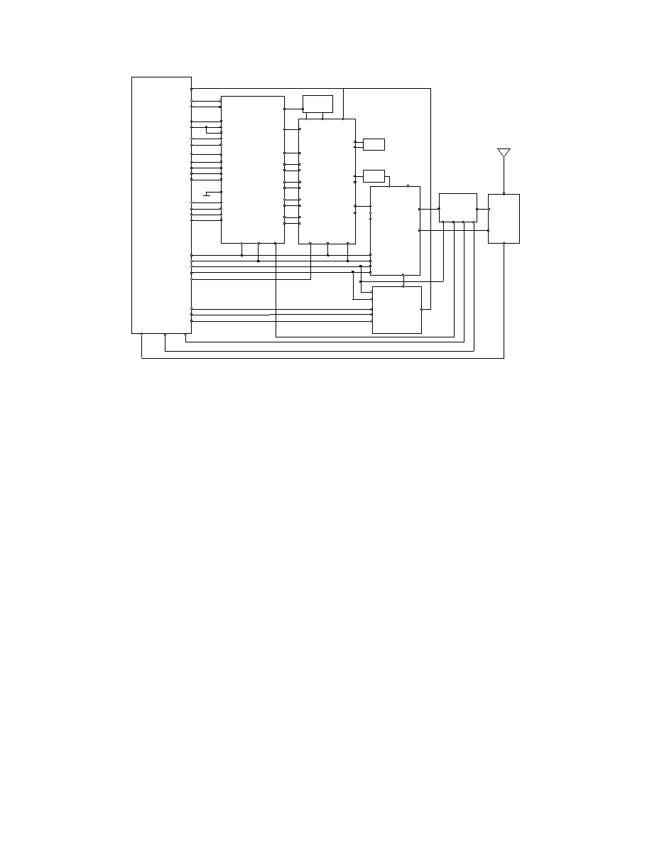
Preliminary Technical Information
AD6426
This Information applies to a product under development. Its characteristics and specifications are subject to change without notice. Analog Devices assumes no
obligation regarding future manufacture unless otherwise agreed to in writing. No responsibility is assumed by Analog Devices for its use; nor for any
infringements of patents or other rights of third parties which may result from its use. No license is granted by implication or otherwise under any patent or patent
rights of Analog Devices.
Revision Preliminary 2.3 (June 9, ´98)
- 21 -
Confidential Information
AFC
BREFOUT
AGC
ITXP
ITXN
QTXP
QTXN
IRXP
IRXN
QRXP
QRXN
RAMP
13 MHz
XTAL
RXON TXON
FILTER
GREF
GAIN
ITXP
ITXN
QTXP
QTXN
IRXP
IRXN
QRXN
QRXP
OSEN RXPU TXPU
FILTER
TMX_OUT
LNA-IN
RXON
TXON
GSM_ON
DCS_ON
RMX_OUT FREF
MXOP
IFHI
RFHI
RFLO
MODP
MODM
XTAL
MCLK
RESET
ASDI
ASDIFS
ASDOFS
ASCLK
ASDO
BSDI
BSDIFS
BSCLK
BSDO
BSDOFS
MODE
VSDI
VSDO
VSCLK
VSFS
CLKOUT
VBCRESET
ASDO
ASOFS
ASCLK
ASDI
BSDO
BSOFS
BSCLK
BSDI
BSIFS
VSDO
VSDI
VSCLK
VSFS
PAs &
Control
FILTERS
ANTENNASELECT
RX
TX
DUALBAND
RF FRONT-END
AD6432
AD6425
RXON
TXENABLE
GPIO2
GPIO1
RADIOPWRCTL
SYNTHCLK
SYNTHDATA
SYNTHEN0
AD6426
BANDSELECT0
BANDSELECT1
TCOR
RFCLK
TX_IN
TXPA
TXPHASE
DCLK
DATA
ENB
GPIO7
RFLO
RFLO
RFCLK
VCOs
+
SYNTHESIZERS
GSM_ON
DCS_ON
CLKIN
Figure 6. EVBC and Radio Interface

Preliminary Technical Information
AD6426
This Information applies to a product under development. Its characteristics and specifications are subject to change without notice. Analog Devices assumes no
obligation regarding future manufacture unless otherwise agreed to in writing. No responsibility is assumed by Analog Devices for its use; nor for any
infringements of patents or other rights of third parties which may result from its use. No license is granted by implication or otherwise under any patent or patent
rights of Analog Devices.
Revision Preliminary 2.3 (June 9, ´98)
- 22 -
Confidential Information
Radio Interface
The AD6426 Radio Interface has been designed to support
direct connection to the ADI IF-Chips AD6432, while
providing full backwards compatibility to existing radio
designs interfacing to the AD20msp410 and AD20msp415.
Additionally the AD6426 Radio Interface supports radio
architectures based on Siemens, TTP/Hitachi or Philips RF
chipsets.
The Radio Interface of the AD6426 consists of 16 dedicated
output pins listed in Table 13. Together with two optional
general purpose I/O-pins they provide a flexible interface to a
variety of radio architectures for both 900 MHz and 1800/1900
MHz operation.
Dual Band Control
To support dual band handsets BANDSELECT[1:0] signals
are provided. BANDSELECT0 is multiplexed with GPIO[2],
with the default function of this being GPIO[2].
BANDSELECT1 is multiplexed with GPIO[1], the default
function being GPIO[1].
For Dual Band solutions requiring a single band select bit, the
BANDSELECT0 function is enabled by asserting the BAND
EN bit. In order to set BANDSELECT0 high/low and cause
the radio module to operate in the appropriate band, the least
significant bit (bit 0) of the relevant 32 bit register for
Dynamic Synthesizer 1 must be written, i.e. different values
may be set for Rx, Tx and Monitor but only for Dynamic
Synthesizer 1.
BANDSELECT0 is sampled internally and is valid from the
beginning of data serialization, both for on demand
(immediate) loading and ordinary interrupt driven loading.
The BANDSELECT0 signal will remain in this known state
until the next time there is any serialization of data for
Dynamic Synthesizer 1, when a new sample will be taken of
the least significant bit of the 32 bit synthesizer register
currently being serialized.
Full control is provided over the number of bits to be shifted
out to the synthesizer and so it is intended that this bit count
will always be less than 32 when using the BANDSELECT0
feature in order to prevent shifting the control bit out.
BANDSELECT0 is gated with RADIO POWER CONTROL to
ensure that whenever the RADIO is off, BANDSELECT0 is
forced to a low state.
For Dual Band Solution requiring two band select bits, one for
GSM900, and one for DCS1800, then both BANDSELECT0
and BANDSELECT1 are enabled by asserting both the BAND
EN and DCSSEL EN bits. The BANDSELECT0 output is
driven as in the single enable mode (described above), and the
BANDSELECT1 output is the inverted output of the raw
BANDSELECT0 output (prior to gating with RADIO POWER
CONTROL), gated with RADIO POWER CONTROL to force
a low output when the Radio is off.
In order to increase the flexibility of the AD6426, three pins in
the Radio Interface are multiplexed with GPO functions. The
pins multiplexed are: SYTHEN1, AGCA and AGCB, with the
default function being the Radio Interface.
The mode of these pins is controlled by the new ccGPO
Channel Codec Register:
The GPO[n]Sel bit selects the function of the pin. Setting
GPO[n]Sel to one will enable the pin to be controlled by the
GPO[n] bit. The GPO[n]Sel bit will override any other pin
function selection.
Generic Pins
The following three pins have the same functionality in all
types of radio architectures:
RADIOPWRCTL
This output signal is typically used to power down the
oscillators and prescalers during Idle mode and is directly
controlled by the Radio Power Control flag in the POWER
CONTROL EXTERNAL CC Control Register 45.
Bit
POWER CONTROL EXTERNAL CC Control
Register 45
1
Radio Power Control
Table 13. Radio Interface
Name
I/O
Function
GPIO1
O
BANDSELECT1
GPIO2
O
BANDSELECT0
RADIOPWRCTL
O
Radio Powerdown Control
GPIO6
O
VBIAS
GPIO7
O
ANTENNASELECT
TXPHASE
O
Switches PLLs (Rx / Tx)
TXENABLE
O
Transmit Enable
TXPA
O
Power Amplifier Enable
RXON
O
Receiver on
CALIBRATERADIO
O
Radio Calibration
SYNTHEN0
O
Synthesizer 0 Enable
SYNTHEN1
O
Synthesizer 1 Enable
SYNTHDATA
O
Synthesizer Port Serial Data
SYNTHCLK
O
Synthesizer Port Clock
AGCA
O
AGC Control A
AGCB
O
AGC Control B
Preliminary Technical Information
AD6426
This Information applies to a product under development. Its characteristics and specifications are subject to change without notice. Analog Devices assumes no
obligation regarding future manufacture unless otherwise agreed to in writing. No responsibility is assumed by Analog Devices for its use; nor for any
infringements of patents or other rights of third parties which may result from its use. No license is granted by implication or otherwise under any patent or patent
rights of Analog Devices.
Revision Preliminary 2.3 (June 9, ´98)
- 23 -
Confidential Information
GPIO6 - VBIAS
This general purpose I/O pin can be used to control the
powering up/down of a separate voltage converter, which may
be needed to provide the supply voltage for GaAs RF Power
Amplifiers. Significant turn-on time of the voltage converter
requires an early power-up signal, which is provided by
GPIO6. This control is achieved entirely through a software
driver, without hardware support. Since this function is not
needed for all radio solutions, the GPIO pin can be used for
other functions if not required.
GPIO7 - ANTENNASELECT
This general purpose I/O pin can be used to switch between
two different antennas, as required, when the mobile radio is
used in conjunction with a car-kit with external antenna. This
control is achieved entirely through a software driver, without
hardware support. Since this function is not needed for all
radio solutions, the GPIO pin can be used for other functions if
not required.
Tx Timing Control
The following 5 radio interface pins serve different functions
depending on the radio architecture:
TXPHASE
The purpose of this signal is to switch PLLs between Rx and
Tx modes. The signal is generated under control of the flags
TXPHASE Enable and TXPHASE Polarity of the RADIO
CONTROL CC Control Register 2.
Bit
RADIO CONTROL CC Control Register 2
6
TXPHASE Polarity
Controls the polarity of the output TXPHASE.
When set to 1, TXPHASE is active low;
When set to 0, TXPHASE is active high.
3
TXPHASE Enable
Enables the output pin TXPHASE if set to 1.
0
Transmit Enable
Enables the output pin TXENABLE if set to 1.
In radios based on the TTP/Hitachi solution, this signal can be
used to switch the VCO´s.
In radios based on the Siemens or Philips solution, this signal
can be used for control switching PLLs, or band switching
UHF PLLs.
TXENABLE
This signal enables the RF modulator and transmit chain
including the PA, and controls the TXON-pin of the AD6425.
The signal is generated under control of flag Transmit Enable
of the RADIO CONTROL CC Control Register 2.
TXPA
This signal is used as a power amplifier (PA) enable and/or as
a control signal for the PA control loop. This allows the PA to
be isolated from the supply outside the Tx-slot to save current.
In the PA control loop it can be used to control the dynamics
of the loop. The flag Tx Pa Polarity in the TRAFFIC MODE
CC Control Register 6, provides independent control for the
TXPA signal.
Bit
TRAFFIC MODE CC Control Register 6
7
Tx Pa Polarity;
active high, when reset
TXPA is derived from the leading edge of TXENABLE signal
shown in Figure 7.
TXENABLE
TXPA
T
D
T
W
Figure 7. Timing of TXPA
The parameter T
D
is a programmable delay (0 to 1023 Q
BIT
) to
accommodate the EVBC settling time. T
D
is therefore a 10 bit
value, accessed via the TXPA OFFSET 1 CC Control Register
73 and the TXPA OFFSET 2 CC Control Register 74.
Bit
TXPA OFFSET 1 CC Control Register 73
1 : 0
TD (9:8)
Bit
TXPA OFFSET 2 CC Control Register 74
7 : 0
TD (7:0)
The parameter T
W
is a programmable width (0 to 1023 Q
BIT
)
which defines the PA enable time. T
W
is therefore a 10 bit
value, accessed via the TXPA WIDTH 1 CC Control Register
75 and the TXPA WIDTH 2 CC Control Register 76.
Bit
TXPA WIDTH 1 CC Control Register 75
1 : 0
TW (9:8)
Bit
TXPA WIDTH 2 CC Control Register 76
7 : 0
TW (7:0)
If T
W
is set to zero, then TXPA will be disabled.
Preliminary Technical Information
AD6426
This Information applies to a product under development. Its characteristics and specifications are subject to change without notice. Analog Devices assumes no
obligation regarding future manufacture unless otherwise agreed to in writing. No responsibility is assumed by Analog Devices for its use; nor for any
infringements of patents or other rights of third parties which may result from its use. No license is granted by implication or otherwise under any patent or patent
rights of Analog Devices.
Revision Preliminary 2.3 (June 9, ´98)
- 24 -
Confidential Information
Rx Timing Control
RXON
The signal at the output pin RXON is generated by the
function Receive Enable OR Monitor Enable of the RADIO
CONTROL CC Control Register 2. It can be used to enable
the RF receiver and controls the RXON-pin of the AD6425. In
radios based on the Siemens solution this signal would be
connected to the RXON1 input. Additional RXON derived
signals are provided to support this solution.
Bit
RADIO CONTROL CC Control Register 2
2
Monitor Enable
1
Receive Enable
CALIBRATERADIO
The 4 modes of the Autocalibrate signal (Type 0 & 1, AutoCal
on/off) are provided as required by the ADI or Philips solution
and shown in Figure 8.
TYPE=0, AUTOCAL=0
TYPE=0, AUTOCAL=1
TYPE=1, AUTOCAL=0
TYPE=1, AUTOCAL=1
RxEnable
Start (late)
RxEnableEnd
AutoCalibrateEnd
RxEnable
Start (early)
RXON
Figure 8. Autocalibration
The flags Autocalibrate and Calibrate Radio in the SYSTEM
CC Control Register 0 are OR´ed and connected to the output
pin CALIBRATERADIO.
Bit
the SYSTEM CC Control Register 0
7
Autocalibrate
Enables the autocalibrate function if set to 1;
3
Calibrate Radio
The type of autocalibration is set in the TRAFFIC MODE CC
Control Register 6
Bit
TRAFFIC MODE CC Control Register 6
3
Autocalibration Type
In radios based on the Siemens chipset, this signal would
connect to the RXON2 input. The required behavior is enabled
by selecting the Type 1 CalibrateRadio function.
Synthesizer Control
The radio interface of the AD6426 supports 2 dynamic
synthesizers, with each capable of downloading data on
demand.
The two Synthesizer Load Dynamic flags located in the
SYNTH CONTROL CC Control Register 38, will set the
synthesizer interface to load 3 consecutive long-words from
Layer 1.
Bit
SYNTH CONTROL CC Control Register 38
7
Synthesizer Enable Polarity
Selects the polarity of the SYNTHEN outputs.
If set to 0, SYNTHEN is an active low signal,
if set to 1, SYNTHEN is an active high signal.
6
Synthesizer Enable Type
Selects the active period of the SYNTHEN outputs.
When set to 0, SYTHEN is active for all data values
determined by SYNTHESIZER BIT COUNT; when
set to 1, SYNTHEN goes active after the last bit for
one SYNTHCLK period.
2
Synthesizer Load Dynamic 1 (SLD1)
1
Synthesizer Load Dynamic 0 (SLD0)
When using the Configure Dynamic Synthesizer flag in the
SYNTH BIT COUNT CC Control Register 37, the download-
on-demand function is applied to the synthesizer selected by
SLD0 or SLD1.
Bit
SYNTH BIT COUNT CC Control Register 37,
6
Configure Dynamic Synthesizer
Each dynamic synthesizer is comprised of three 32-bit word
registers, for the Rx, Tx and Monitor phases. The download
on demand uses the Rx register only for the respective
synthesizer.
Bit
SYNTHESIZER 1 CC Control Register 40
7 : 0
Synthesizer (31:24)
Bit
SYNTHESIZER 2 CC Control Register 41
7 : 0
Synthesizer (23:16)
Bit
SYNTHESIZER 3 CC Control Register 42
7 : 0
Synthesizer (15:8)
Bit
SYNTHESIZER 4 CC Control Register 43
7 : 0
Synthesizer (7:0)
Preliminary Technical Information
AD6426
This Information applies to a product under development. Its characteristics and specifications are subject to change without notice. Analog Devices assumes no
obligation regarding future manufacture unless otherwise agreed to in writing. No responsibility is assumed by Analog Devices for its use; nor for any
infringements of patents or other rights of third parties which may result from its use. No license is granted by implication or otherwise under any patent or patent
rights of Analog Devices.
Revision Preliminary 2.3 (June 9, ´98)
- 25 -
Confidential Information
The two dynamic synthesizers are programmable as follows,
while each synthesizer may be independently disabled,
through the two Disable Synthesizer flags in the
SYNTHESIZER PROGRAM CC Control Register 72.
Bit
SYNTHESIZER PROGRAM CC Control Register
72
5
Disable Synthesizer 1
4
Disable Synthesizer 0
3
Synthesizer Enable Select
2
Synthesizer Mode
1 : 0
Pin Mode (1:0)
SYNTHEN0 : 1
The AD6426 provides enable signals for two independent
synthesizers. These signals are available at the output pins
SYNTHEN0 and SYNTHEN1. The polarities of these signals
are individually programmable; i.e. bit 7 of CC Control
Register 38 is applied to the synthesizer selected by either bit
2 or bit 1 of the same register.
SYNTHDATA and SYNTHCLK
Three Modes can be selected to support different radio
architectures. The selection of the Pin-Mode is done by the
two Pin Mode flags in the SYNTHESIZER PROGRAM CC
Control Register 72 as shown in Table 14.
Table 14. Pin Mode
Bit 1
Bit 0
Mode
0
0
Mode 1 (default)
0
1
Mode 1
1
0
Mode 2
1
1
Mode 3
The default is Mode 1, which supports TTP/Hitachi Bright
and Philips radio architectures. Mode 2 also supports a Philips
architecture, while Mode 3 supports a Siemens architecture. In
Mode 1, the pins SYNTHDATA and SYNTHCLK have their
original functionality; i.e. SYNTHDATA is the data output
and SYNTHCLK is the clock output of the serial synthesizer
interface. Clock polarity and frequency are programmed in the
SYNTH CONTROL CC Control Register 38.
Table 15. Pin Function in Mode 1
AD6426 Pin
Function
SYNTHDATA
Synthesizer Data
SYNTHCLK
Synthesizer Clock
Bit
SYNTH CONTROL CC Control Register 38
5
Synthesizer Clock Polarity
Selects the edge, on which synthesizer data and
enable will be clocked out. Negative edge, when set
to 0; positive edge, when set to 1.
0
Synthesizer Clock;
selects the frequency of SYNTHCLK output.
SYNTHCLK = 1.625 MHz if set to 0 (default),
SYNTHCLK = 6.5 MHz if set to 1.
In Modes 2 and 3, the outputs of these two pins are
multiplexed with flags of the internal DSP as indicated in
Table 16. The function of DSPFLAG1 ô Synthesizer Data is
defined as: The output is that of DSPFLAG1 except when the
synthesizer interface is active. In this case the synthesizer
output has priority. The same applies to DSPFLAG2 ô
Synthesizer Clock.
Table 16. Pin Function in Modes 2 and 3
AD6426 Pin
Function
SYNTHDATA
DSPFLAG1 ô Synthesizer Data
SYNTHCLK
DSPFLAG2 ô Synthesizer Clock
AGC Control
AGC programming is achieved in one of three ways:
The first is a gain select approach, whereby the DSPFLAG0
and DSPFLAG1 are used as a 2-bit gain selector (AGCA,
AGCB). This is available in Mode 1 and the flags are under
direct control of the internal DSP and are timing independent
of the synthesizer interface.
Table 17. Pin Function in Mode 1
AD6426 Pin
Function
AGCA
DSPFLAG0
AGCB
DSPFLAG1
The second is through the DSP combined with the serial
synthesizer interface, as defined in Mode 2. The function of
DSPFLAG0 ô SYNTHEN1 is defined as: The output is that of
DSPFLAG0 except when the synthesizer interface is active.
To support the Philips chipset whereby the AGC and the PLL
are programmed over the same enable line, the AGCA pin is
multiplexed to provide a SYNTHEN1 gated with DSPFLAG0.
This pin would be wired instead of the SYNTHEN1 pin. Since
the DSP would program the AGC during RXON, and the
synthesizers are reprogrammed following the end of the active
phase, no conflict can occur.
Preliminary Technical Information
AD6426
This Information applies to a product under development. Its characteristics and specifications are subject to change without notice. Analog Devices assumes no
obligation regarding future manufacture unless otherwise agreed to in writing. No responsibility is assumed by Analog Devices for its use; nor for any
infringements of patents or other rights of third parties which may result from its use. No license is granted by implication or otherwise under any patent or patent
rights of Analog Devices.
Revision Preliminary 2.3 (June 9, ´98)
- 26 -
Confidential Information
In Modes 2 and 3, PLL programming occurs on any of Rx, Tx
and MonEnableEnd through the synthesizer interface.
Additionally, AGC programming, controlled via the DSP, is
performed during RXON.
Table 18. Pin Function in Mode 2
AD6426 Pin
Function
AGCA
DSPFLAG0 ô SYNTHEN1
AGCB
DSPFLAG1
The third mode is for support of the Siemens chipset,
providing an independent AGC enable from SYNTHEN using
the DSP Flag 0. The same serial interface constraints from
Mode 2 apply. Additionally, the output OCE is provided. This
is the Offset Correction Enable, derived from the
RxEnableStartEarly and RxEnableStartLate timing signals as
shown in Figure 9.
Table 19. Pin Function in Mode 3
AD6426 Pin
Function
AGCA
DSPFLAG0
AGCB
OCE
RxEnableStartEarly
RxEnableStartLate
RXON
OCE
Figure 9. OCE Signal
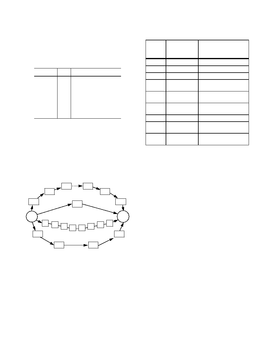
Preliminary Technical Information
AD6426
This Information applies to a product under development. Its characteristics and specifications are subject to change without notice. Analog Devices assumes no
obligation regarding future manufacture unless otherwise agreed to in writing. No responsibility is assumed by Analog Devices for its use; nor for any
infringements of patents or other rights of third parties which may result from its use. No license is granted by implication or otherwise under any patent or patent
rights of Analog Devices.
Revision Preliminary 2.3 (June 9, ´98)
- 27 -
Confidential Information
TEST INTERFACE
The AD6426 provides a complete JTAG test interface. The
functionality of these pins are shown in Table 20.
Furthermore, these pins can assume a different functionality
described in detail in the chapter MODES OF OPERATION.
Table 20. Test Interface
Name
I/O
Function
JTAGEN
I
JTAG enable (internal pull
down resistor)
TCK
I
JTAG test clock input
TMS
I
JTAG test mode select
TDI
I
JTAG test data input
TDO
O
JTAG test data output
JTAG Port
The AD6426 provides full IEEE 1149.1 compliance. The
JTAG Port must be run at a frequency of 5 MHz or less.
The JTAG Port is explicitly enabled through JTAGEN. When
disabled, the corresponding pins are re-used for the AD6426
Feature Modes. The JTAG interface implements four registers
shown in Figure 10. The content of the Instruction register
selects one of these four registers.
3
161
2
3
163
1
162
2
1
T D O
1
4
Boundary Register
Bypass Register
Instruction Register
T D I
Bist Register
1
2
3
4
5
6
7
8
Figure 10. JTAG Registers
The instruction register contains 4 bits, and supports the
instructions listed in Table 21.
Instruction register values 01XX all select the bypass register
when JTAG compliance is enabled. Values 00XX control the
AD6426 I/O as defined in Mode A, and therefore should not
be used in any other mode.
Table 21. JTAG Instructions
Instr.
Register
4 3 2 1
Code
Comments
0 0 0 0
ExTest
Public Instruction
0 0 0 1
Clamp
Optional Public Instruction
0 0 1 0
Sample/PreLoad
Public Instruction
0 0 1 1
DoBist
Private Instruction
Engineering Mode Test
0 1 0 0 -
0 1 0 1
Reserved
0 1 1 0
Mode D
Private Instruction
H8 Emulation
0 1 1 1
Reserved
1 0 0 0 -
1 1 1 0
Bypass
Public Instruction
Selects Mode A
1 1 1 1
Bypass
Public Instruction
Selects Mode A (default)
ExTest Instruction
The ExTest instruction is used to force input or output
conditions on the boundary scan cell.
Clamp Instruction
This optional public instruction is similar to the Bypass
instruction, except that once loaded, it will force the values
held in the boundary scan chain onto the corresponding
outputs of the device. This enables all output and bi-
directional pads to be fixed, allowing other parts on the PC-
board to be tested without interference from the AD6426,
while at the same time selecting the Bypass register for the
shortest possible scan path.
All input activity to the AD6426 will be ignored during this
time, since all inputs are driven from the preloaded values in
the boundary scan chain. Typically therefore this instruction
would be preceded by the Sample/Preload instruction. This
instruction is only valid during the normal operation of the
AD6426; i.e. in Mode A.
Sample/Preload Instruction
The Sample/Preload instruction is fully IEEE compliant.
Boundary Register
The boundary cell structure is based on the I/O definition in
Mode A, and hence pins which are outputs only in this mode,
but become inputs in another mode, do not support input scan
cells, and vice versa. Table 22 shows the complete Boundary
register.
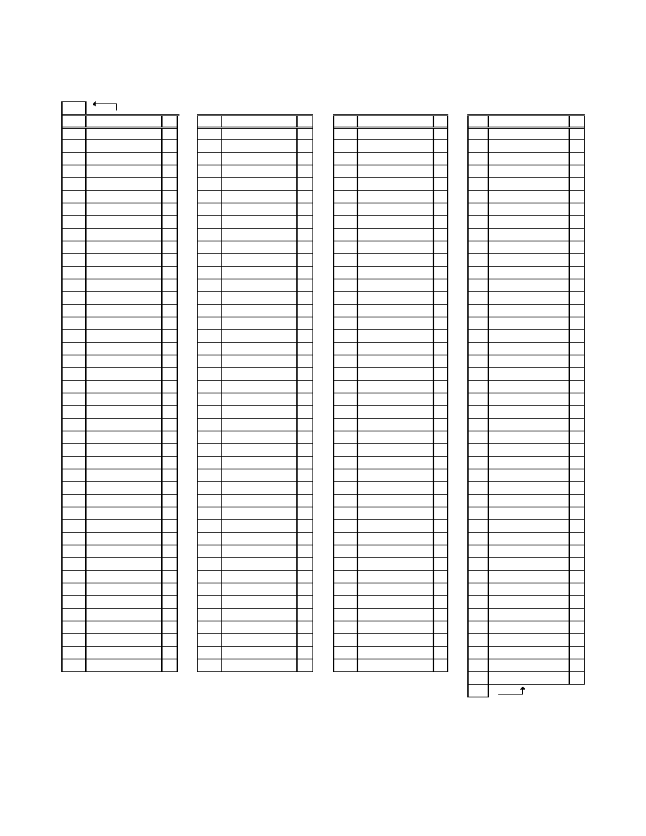
Preliminary Technical Information
AD6426
This Information applies to a product under development. Its characteristics and specifications are subject to change without notice. Analog Devices assumes no
obligation regarding future manufacture unless otherwise agreed to in writing. No responsibility is assumed by Analog Devices for its use; nor for any
infringements of patents or other rights of third parties which may result from its use. No license is granted by implication or otherwise under any patent or patent
rights of Analog Devices.
Revision Preliminary 2.3 (June 9, ´98)
- 28 -
Confidential Information
Table 22. Boundary Scan Path
TDO
#
Cell Name
1
SIMCARD
B
2
SIMCARD
O
3
SIMCARD
I
4
SIMCLK
O
5
SIMDATAOPEN
T
6
SIMDATAOP
O
7
SIMDATAIP
I
8
SIMRESET
O
9
SIMPROG
B
10
SIMPROG
O
11
SIMPROG
I
12
SIMSUPPLY
O
13
GPIO0EN
B
14
GPIO0
O
15
GPIO0
I
16
GPIO1EN
B
17
GPIO1
O
18
GPIO1
I
19
WR
O
20
FLASHPWD
B
21
FLASHPWD
O
22
FLASHPWD
I
23
DATA0 : 7EN
B
24
DATA0
O
25
DATA0
I
26
DATA1
O
27
DATA1
I
28
DATA2
O
29
DATA2
I
30
DATA3
O
31
DATA3
I
32
DATA4
O
33
DATA4
I
34
DATA5
O
35
DATA5
I
36
DATA6
O
37
DATA6
I
38
DATA7
O
39
DATA7
I
40
LBS
O
41
UBS
O
42
RD
O
43
DATA8 : 15 EN
B
#
Cell Name
44
DATA8
O
45
DATA8
I
46
DATA9
O
47
DATA9
I
48
DATA10
O
49
DATA10
I
50
DATA11
O
51
DATA11
I
52
DATA12
O
53
DATA12
I
54
DATA13
O
55
DATA13
I
56
DATA14
O
57
DATA14
I
58
DATA15
O
59
DATA15
I
60
ROMCS
O
61
RAMCS
O
62
ADD0
O
63
ADD1
O
64
ADD2
O
65
ADD 3
O
66
ADD4
O
67
ADD5
O
68
ADD6
O
69
ADD7
O
70
ADD8
O
71
BOOTCODEEN
I
72
ADD9
O
73
ADD10
O
74
ADD11
O
75
ADD12
O
76
ADD13
O
77
ADD14
O
78
ADD15
O
79
ADD16
O
80
ADD17
O
81
ADD18
O
82
ADD19
O
83
ADD20
O
84
USCRTS
I
85
USCCTSEN
B
86
USCCTS
O
#
Cell Name
87
USCCTS
I
88
USCTX
O
89
USCRXEN
B
90
USCRX
O
91
USCRX
I
92
USCRI
I
93
GPIO9EN
B
94
GPIO9
O
95
GPIO9
I
96
GPIO8EN
B
97
GPIO8
O
98
GPIO8
I
99
IRQ6
I
100
RESET
I
101
KEYPADROW0
I
102
KEYPADROW1
I
103
KEYPADROW2
I
104
KEYPADROW3
I
105
KEYPADROW4
I
106
KEYPADROW5
I
107
KEYPADCOL0EN
T
108
KEYPADCOL0
O
109
KEYPADCOL1EN
T
110
KEYPADCOL1
O
111
KEYPADCOL2EN
T
112
KEYPADCOL2
O
113
KEYPADCOL3EN
T
114
KEYPADCOL3
O
115
GPCS
O
116
OSC13MON
O
117
BACKLIGHT
O
118
DISPLAYCS
O
119
LCDCTL
O
120
GPIO3EN
B
121
GPIO3
O
122
GPIO3
I
123
GPIO4EN
B
124
GPIO4
O
125
GPIO4
I
126
GPIO5EN
B
127
GPIO5
O
128
GPIO5
I
129
GPIO6EN
B
#
Cell Name
130 GPIO6
O
131 GPIO6
I
132 GPIO7EN
B
133 GPIO7
O
134 GPIO7
I
135 CLKIN
I
136 TXENABLE
O
137 RADIOPWRCTL
O
138 CALIBRATERADIO
O
139 TXPA
O
140 AGCB
O
141 AGCA
O
142 SYNTHCLK
O
143 SYNTHDATA
O
144 SYNTHEN0
O
145 SYNTHEN1
O
146 PWRON
O
147 OSCIN
I
148 GPIO2EN
B
149 GPIO2
O
150 GPIO2
I
151 TXPHASE
O
152 ASDO
O
153 ASOFS
O
154 ASDI
I
155 ASCLK
O
156 BSCLK
I
157 BSDI
I
158 BSIFS
I
159 BSOFS
O
160 BSDO
O
161 CLKOUT
O
162 RXON
O
163 VBCRESET
O
164 VSCLK
I
165 VSDI
I
166 VSFS
I
167 VSDOEN
T
168 VSDO
O
169 EEPROMDATAEN
B
170 EEPROMDATA
O
171 EEPROMDATA
I
172 EEPROMCLK
O
173 EEPROMEN
O
TDI
Notes: The boundary scan supports only pin functionality and signal directions of Normal Mode (A); see chapter "Modes of Operation". Cells can be input (I) or output cells (O) which
correspond to the pins with the same name, or internal control cells shown in ITALIC. Control cells are either bi-directional control cells (B), or tri-state output control cells (T). When
type-B cells are loaded with 0, the referred pins become driving output pins, otherwise the pins are inputs. When type-T cells are loaded with 1, the referred pin will be tri-stated,
otherwise the pin is an output.
Preliminary Technical Information
AD6426
This Information applies to a product under development. Its characteristics and specifications are subject to change without notice. Analog Devices assumes no
obligation regarding future manufacture unless otherwise agreed to in writing. No responsibility is assumed by Analog Devices for its use; nor for any
infringements of patents or other rights of third parties which may result from its use. No license is granted by implication or otherwise under any patent or patent
rights of Analog Devices.
Revision Preliminary 2.3 (June 9, ´98)
- 29 -
Confidential Information
DoBist Instruction
This instruction is provided to support engineering mode test.
When the instruction is loaded, it will generate an NMI to the
H8 processor. This will enable special software to be executed
which can be used to test the operation of the device. During
this time, the 8-bit DoBist register is selected for scan,
enabling a result code for the test to be scanned out. For the
duration of the test, all I/O retain their normal function. The
test program must therefore cope with undefined inputs, but is
able to communicate with other devices to extend the test
procedure. This allows the NMI to be generated during normal
phone operation. This instruction is only valid during the
normal operation of the AD6426; i.e. in Mode A.
Mode D Instruction
This instruction switches the AD6426 into the H8 Emulation
Mode (Mode D). It is only valid to switch modes while the
AD6426 is held in reset.
Reset
To comply with the IEEE specification, the JTAG interface
will be forced to reset whenever the JTAG Port is re-enabled.
This will select the Bypass register and force the AD6426 into
the Normal Mode (Mode A).
Debug Port Interface
In normal (voice-service) operation, the Universal Serial Port
can be used as a monitor port, which allows monitoring
internal operation of the channel codec section. However,
during the use of GSM Data Services, the USC is engaged in
data communication and cannot be used for monitoring. The
6426 provides a Debug Port to enable monitoring and
debugging in this case. This is in the form of a simple 2 pin
UART. The communication format is fixed at 9600 baud, 8
data bits, one stop bit, no parity, asynchronous
communication. Operation of the Debug Port is under control
of the Layer 1 software.
Two of the GPIO pins can be programmed to be used as the
Debug Port:
Pin Name
New Function
GPIO8
TXDATA
GPIO9
RXDATA
The serial port can be enabled by asserting the flag DATA
SERIAL PORT SELECT in CC Control Register 7.
MODES OF OPERATION
The AD6426 can be switched between two main operating
modes, using instructions downloaded via the JTAG interface.
This must be done while the AD6426 is held in reset. Once
the instruction load is completed the pins are immediately set
to reflect the new operating mode. Table 23 shows these
modes. The modes B and C are reserved and are not available
to the user.
Table 23. Modes of Operation
Mode of Operation
A
Normal Mode
B
Reserved
C
Reserved
D
Emulation Mode (H8)
Normal Mode (Mode A)
This mode is used during normal operation of the AD6426. All
JTAG-pins have their normal functionality, when enabled by
JTAGEN and can be used for production test.
Emulation Mode (Mode D)
Selecting Mode D allows the emulation of the internal H8
processor. In this Mode several pins assume a new
functionality or are no longer available. Table 24 lists all pins,
which have different functionality or direction in the
Emulation Mode compared to the Normal Mode.
In Emulation Mode the internal DSP remains active but will
not have access to external memory devices. The internal H8
will be switched into hardware stand-by mode; the LCD
controller interface and Boot Code ROM remain functional.
CCIRQ0 : 2 are channel codec interrupts to the emulator.
CCIRQ2 is defined in CC Control Registers 77 and 78.
Table 24. Pin Functions in Mode D
Pin Name in
Normal Mode (A)
Pin Function in
Emulation Mode (D)
IRQ6
CCCS
I
ADD19 : 16
-
TRI
ADD15 : 0
ADD15 : 0
I
DATA7 : 0
-
TRI
RD
RD
I
HWR
HWR
I
LWR
-
TRI
RAMCS
-
TRI
SIMCARD
-
TRI
SIMDATAOP
-
TRI - O
SIMDATAIP
-
I
SIMCLK
-
O
SIMRESET
CCIRQ0
O
SIMPROG
CCIRQ2
O
SIMSUPPLY
CCIRQ1
O
GPIO9
H8CS0
I
GPIO8
CCGPIO8
I/O -
TRI
Preliminary Technical Information
AD6426
This Information applies to a product under development. Its characteristics and specifications are subject to change without notice. Analog Devices assumes no
obligation regarding future manufacture unless otherwise agreed to in writing. No responsibility is assumed by Analog Devices for its use; nor for any
infringements of patents or other rights of third parties which may result from its use. No license is granted by implication or otherwise under any patent or patent
rights of Analog Devices.
Revision Preliminary 2.3 (June 9, ´98)
- 30 -
Confidential Information
Pin Name in
Normal Mode (A)
Pin Function in
Emulation Mode (D)
GPO10
WAIT
O
GPCS
-
TRI
FLASHPWD
Forced High
O
DISPLAYCS
DISPLAYCS
I/O
GPIO0
Reserved
O
GPIO1
Forced High/
BANDSELECT1
O
GPIO2
Forced High/
BANDSELECT0
O
GPIO3
Forced High/DISPA0
O
GPIO4
Forced High/DISPCLK
O
GPIO5
Forced High/BATID
O
GPIO6
Reserved
O
GPIO7
Reserved
TRI
FLASHPWD can also be used as WAIT input, in which case it
is routed through and gated with the LCDWAIT to be output
on the WAIT output pin GPO10/ADD20. If the on-chip LCD
controller is not used in emulation, then ADD20 pin can be
used as ccGPO(10).
FEATURE MODES
Two additional features can be enabled under software
control.
These are; DAI Mode (Digital Audio Interface) and HSL
Mode (High Speed Logging) used to monitor the operation of
the on-chip DSP.
DAI Mode
This mode is selected during type approval, when Digital
Audio Interface is required. To enable this feature, the
JTAGEN pin must be de-asserted, upon which the JTAG pins
TMS, TDI and TDO are re-assigned as shown in Table 25.
The default feature mode thus enabled is DAI. In addition, the
voiceband serial port signals are made available through the
USC to facilitate testing of the speech transcoder as well as
the phone's acoustic properties. The DAI box interface product
is available upon request from Analog Devices.
Table 25. DAI Mode
AD6426 Pin
Function in DAI Mode
I/O
VSCLK
MSCLK
I
VSFS
MSFS
I
VSDO
MSRXD
O
VSDI
MSTXD
I
TMS
DAIRESET
O
TDI
DAI1
O
TDO
DAI0
I
High Speed Logging
This mode is selected for monitoring the operation of the
internal DSP during the development and field test phase.
When the JTAGEN pin is de-asserted and the HSLEnable flag
in the TESTADDRESS CC Control Register 33 is set, a high
speed logging port is mapped on the JTAG- and EEPROM
pins as shown in Table 26. The internal DSP must then be
instructed via Layer 1 to output logging messages onto the
HSL pins.
Table 26. HSL Mode
AD6426 Pin
Function in HSL Mode
TCK
HSLDO0
O
TMS
HSLDO1
O
TDO
HSLDO2
O
TDI
HSLDO3
O
EEPROMCLK
HSLCLK
O
EERPROMEN
HSLFS
O
The High Speed Logging port (HSL) is an unidirectional port
which supplies nibble-wide synchronous data from the internal
DSP to an external data logger. The data logger will be
connected to a PC which will be responsible for presenting the
data to the user. The PC is able to configure the HSL via
either one of the serial interfaces.
The HSL is enabled as follows:
·
The JTAGEN pin is set to 0
·
The H8 enables the HSL logic by setting the HSLEnable
flag
·
On a command issued through the Data Interface, the H8
configures the DSP software to enable HSL
The HSLEnable flag is used to deselect DAIRESET in favor of
the HSL onto the JTAG pins, and enable the HSL onto
EEPROMCLK and EEPROMEN.
The DSP sends data over the port by writing to address 0x000
in the Data Memory map. The writes are full 16-bit writes,
and can occur at a maximum rate of one write per five 39 MHz
clock cycles. Five cycles allow time for the HSL circuit to
serialize the 16 bits of data onto the 4-bit data bus with one
cycle to spare. HSLFS is used to frame the valid data nibbles.
Note that HSCLK is free-running , and that HSLFS and
HSLDO3-0 are synchronized to the rising edge of HSCLK.
Preliminary Technical Information
AD6426
This Information applies to a product under development. Its characteristics and specifications are subject to change without notice. Analog Devices assumes no
obligation regarding future manufacture unless otherwise agreed to in writing. No responsibility is assumed by Analog Devices for its use; nor for any
infringements of patents or other rights of third parties which may result from its use. No license is granted by implication or otherwise under any patent or patent
rights of Analog Devices.
Revision Preliminary 2.3 (June 9, ´98)
- 31 -
Confidential Information
The mapping of the DSP data bits to the HSL port bits is:
Table 27. Mapping of HSL Port Nibbles
DSP
Data Bits
HSLDO
Nibble
23 : 20
1
19 : 16
2
15 : 12
3
11 : 8
4
HSCLK
HSLFS
HSLDO (3:0)
1 2 3 4 1
Figure 11. HSL Timing

Preliminary Technical Information
AD6426
This Information applies to a product under development. Its characteristics and specifications are subject to change without notice. Analog Devices assumes no
obligation regarding future manufacture unless otherwise agreed to in writing. No responsibility is assumed by Analog Devices for its use; nor for any
infringements of patents or other rights of third parties which may result from its use. No license is granted by implication or otherwise under any patent or patent
rights of Analog Devices.
Revision Preliminary 2.3 (June 9, ´98)
- 32 -
Confidential Information
SPECIFICATIONS
General
Parameter
Min
Typ
Max
Units
Comments
T
A
, Ambient Operating Temperature
-25
+85
°C
V
DD
, Supply Voltage
2.4
3.3
Volt
I
DD
, Supply Current (Idle Mode)
TBD
mA
@ V
DD
= 3.0 V
I
DD
, Supply Current (Talk Mode)
TBD
mA
@ V
DD
= 3.0 V
f
CLKIN
, Clock Input Frequency
13
MHz
V
CLKIN
, Clock Input Voltage
0.250
V
PP
sine wave, ac-coupled
R
CLKIN
, Clock Input Resistance (see Note)
19.5
k
sine wave, ac-coupled
Logic Inputs
V
IH
, Input High Voltage
V
DD
- 0.8
Volt
V
IL
, Input Low Voltage
0.8
Volt
I
IH
, I
IL
Input Current
-10
10
µ
A
C
IN
, Input Capacitance
TBD
pF
Logic Outputs
V
OH
, Output High Voltage
V
DD
- 0.4
V
OL
, Output Low Voltage
0.4
I
OZL
, Low Level Output 3-State Leakage Current
-10
10
µ
A
I
OZH
, High Level Output 3-State Leakage Current
-10
10
µ
A
Note:
The input impedance of the clock buffer is a function of the voltage and waveform of the clock input signal. For sinusoidal input
signals the typical input impedance can be calculated by: R
IN
[k
] = V
CLKIN
[V
PP
]
×
78
ABSOLUTE MAXIMUM RATINGS
VDD to GND ............................................. -0.3V to + TBD V
Digital I/O Voltage to GND ................... -0.3V to VDD + 0.3V
Operating Temperature Range ........................ -25°C to +85°C
LQFP Package
Storage Temperature Range .......................... -65°C to +150°C
Maximum Junction Temperature ................................ +150°C
Q
JA
Thermal Impedance..............................................28°C/W
Lead temperature, Soldering
Vapor Phase (60 sec)........................................... +215°C
Infrared (15 sec).................................................. +220°C
PBGA Package
Storage Temperature Range .......................... -65°C to +150°C
Maximum Junction Temperature ................................ +150°C
Q
JA
Thermal Impedance..............................................30°C/W
Lead temperature, Soldering
Vapor Phase (60 sec)........................................... +215°C
Infrared (15 sec).................................................. +220°C
Note:
Stresses above those listed under "Absolute Maximum Ratings" may cause permanent damage to the device. This is a stress rating only and functional
operation of the device at these or any other conditions above those listed in the operational sections is not implied. Exposure to absolute maximum rating
conditions for extended periods may affect device reliability. T
A
= +25°C unless otherwise stated.
ESD SUSCEPTIBILITY
ESD (electrostatic discharge) sensitive device. Electrostatic charges as high as 4000 volts, which
readily accumulate on the human body and on test equipment, can discharge without detection.
Although this device features proprietary ESD protection circuitry, permanent damage may still occur
on this device if it is subjected to high energy electrostatic discharges. Therefore, proper precautions
are recommended to avoid any performance degradation or loss of functionality.
WARNING!
ESD SENSITIVE DEVICE
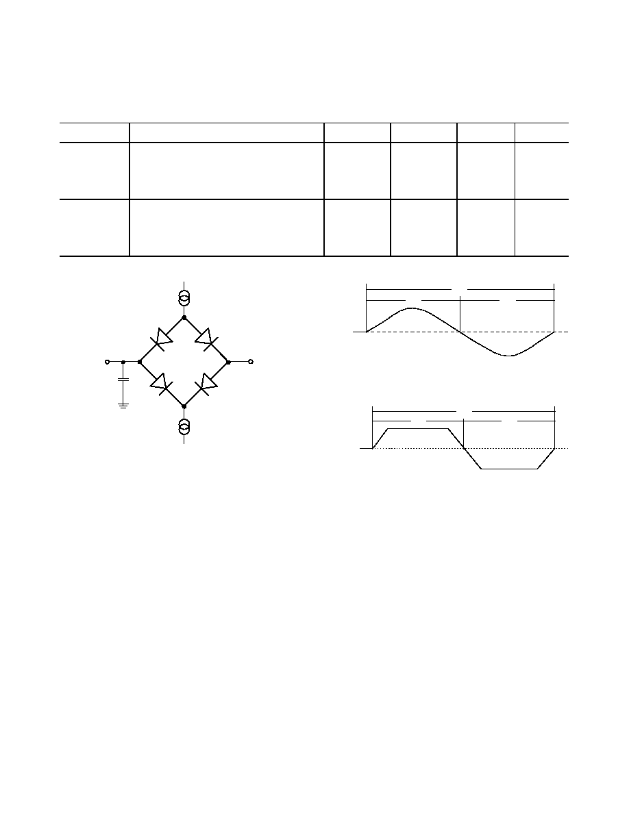
Preliminary Technical Information
AD6426
This Information applies to a product under development. Its characteristics and specifications are subject to change without notice. Analog Devices assumes no
obligation regarding future manufacture unless otherwise agreed to in writing. No responsibility is assumed by Analog Devices for its use; nor for any
infringements of patents or other rights of third parties which may result from its use. No license is granted by implication or otherwise under any patent or patent
rights of Analog Devices.
Revision Preliminary 2.3 (June 9, ´98)
- 33 -
Confidential Information
TIMING CHARACTERISTICS
Clocks
Parameter
Comment
Min
Typ
Max
Units
t
1
CLKIN Period (see Figure 13)
76.9
ns
t
2
CLKIN Width Low
30
45
ns
t
3
CLKIN Width High
30
45
ns
t
4
CLKOUT Period (see Figure 14)
76.9
ns
t
5
CLKOUT Width Low
30
45
ns
t
6
CLKOUT Width High
30
45
ns
To Ouput
Pin
CL
50pF
+2.1V
100
µ
A I
OL
100
µ
A I
OH
Figure 12. Load Circuit for Timing Specifications
t
2
t
3
t
1
CLKIN
Figure 13. Clock Input
t
5
t
6
t
4
CLKOUT
Figure 14. Clock Output
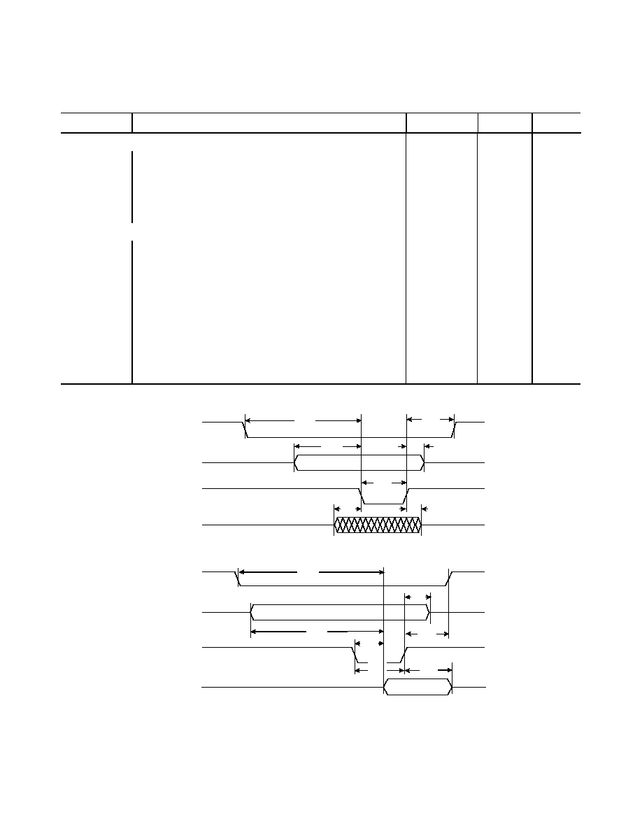
Preliminary Technical Information
AD6426
This Information applies to a product under development. Its characteristics and specifications are subject to change without notice. Analog Devices assumes no
obligation regarding future manufacture unless otherwise agreed to in writing. No responsibility is assumed by Analog Devices for its use; nor for any
infringements of patents or other rights of third parties which may result from its use. No license is granted by implication or otherwise under any patent or patent
rights of Analog Devices.
Revision Preliminary 2.3 (June 9, ´98)
- 34 -
Confidential Information
TIMING SPECIFICATION
Memory Interface
Parameter
Comment ( Timing for 3-state access, see Figure 15 )
Min
Max
Units
Timing Requirement
t
10b
Control Processor read chip select to data valid
158
ns
t
12b
Control Processor read address to data valid
162
ns
t
17
Control Processor read enable to data valid
129
ns
t
19
Control Processor data hold
0
ns
Switching Characteristic
t
10a
Control Processor write chip select setup
10
ns
t
11
Control Processor chip select hold
5
ns
t
12a
Control Processor write address setup
10
ns
t
13
Control Processor address hold
5
ns
t
14
Control Processor write pulse width
111
ns
t
15
Control Processor data setup
68
ns
t
16
Control Processor data hold
15
ns
t
18
Control Processor read pulse width
145
ns
WRITE
CS
ADD 15:0
HWR/LWR
DATA15:0
t
10a
READ
CS
ADD15:0
RD
DATA7:0
t
11
t
12a
t
13
t
14
t
15
t
16
t
10b
t
11
t
17
t
12b
t
13
t
19
t
18
Figure 15. Memory Interface Timing
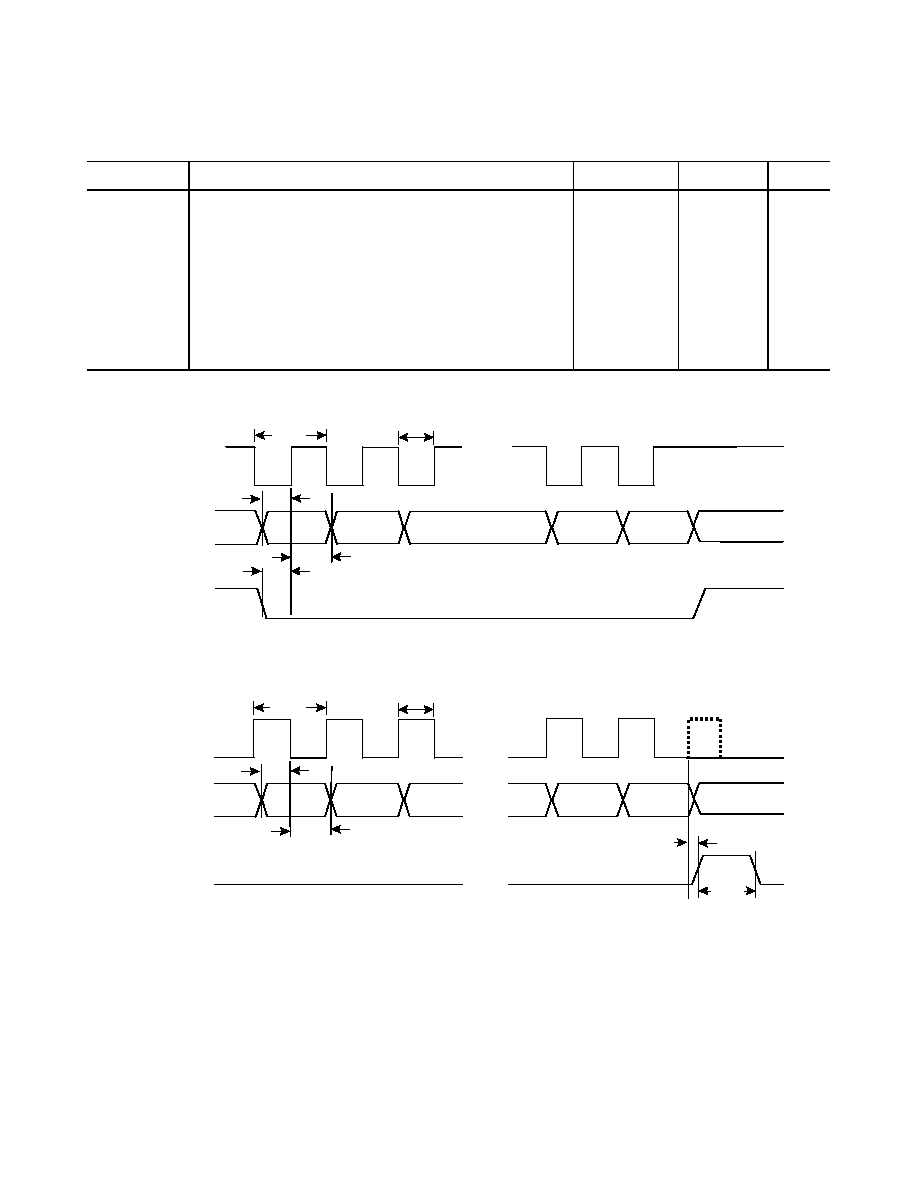
Preliminary Technical Information
AD6426
This Information applies to a product under development. Its characteristics and specifications are subject to change without notice. Analog Devices assumes no
obligation regarding future manufacture unless otherwise agreed to in writing. No responsibility is assumed by Analog Devices for its use; nor for any
infringements of patents or other rights of third parties which may result from its use. No license is granted by implication or otherwise under any patent or patent
rights of Analog Devices.
Revision Preliminary 2.3 (June 9, ´98)
- 35 -
Confidential Information
TIMING CHARACTERISTICS
Radio Interface
Parameter
Comment ( see Figure 16 )
Min
Max
Units
t
40
Synthesizer clock period
152
615
ns
t
41
Synthesizer clock high
76
307
ns
t
42a
Synthesizer data setup
60
85
ns
t
42b
Synthesizer data hold
60
85
ns
t
43a
Synthesizer enable delay for Type 0
60
85
ns
t
43b
Synthesizer enable delay for Type 1
-15
10
ns
t
44
Synthesizer enable width for Type 1
50
90
ns
SYNTHCLK
SYNTHDATA
SYNTHEN[0:1]
TYPE 0
0 1 2 n-2 n-1 n
t
40
t
41
t
42a
t
43a
t
42b
SYNTHCLK
SYNTHDATA
SYNTHEN[0:1]
TYPE 1
0 1 2 n-2 n-1 n
t
44
t
43b
t
42b
t
42a
t
40
t
41
Figure 16. Synthesizer Interface Timing
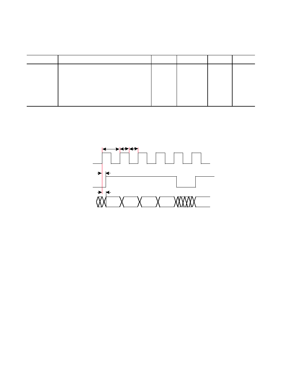
Preliminary Technical Information
AD6426
This Information applies to a product under development. Its characteristics and specifications are subject to change without notice. Analog Devices assumes no
obligation regarding future manufacture unless otherwise agreed to in writing. No responsibility is assumed by Analog Devices for its use; nor for any
infringements of patents or other rights of third parties which may result from its use. No license is granted by implication or otherwise under any patent or patent
rights of Analog Devices.
Revision Preliminary 2.3 (June 9, ´98)
- 36 -
Confidential Information
TIMING CHARACTERISTICS
High Speed Logging Interface
Parameter
Comment ( see Figure 17)
Min
Typ
Max
Units
t
50
HSCLK Period
25.6
ns
t
51
HSCLK Width Low
8.3
ns
t
52
HSCLK Width High
8.3
ns
t
53
HSCLK to HSLDO
0
15
ns
t
54
HSCLK to HSLFS
0
15
ns
HSLDO3:0
HSCLK
HSLFS
1 2 3 4 1
t
50
t
51
t
52
t
54
t
53
Figure 17. High Speed Logging Interface
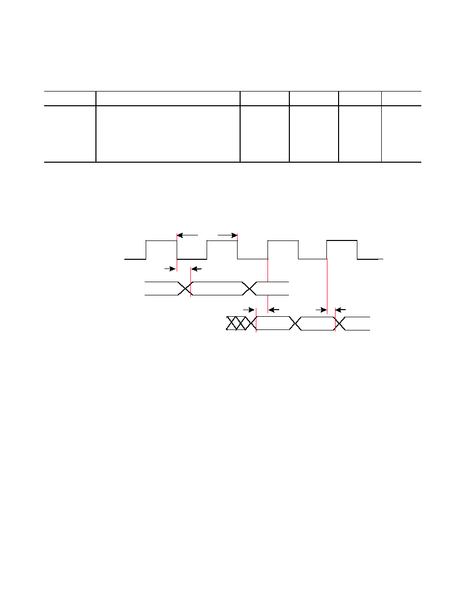
Preliminary Technical Information
AD6426
This Information applies to a product under development. Its characteristics and specifications are subject to change without notice. Analog Devices assumes no
obligation regarding future manufacture unless otherwise agreed to in writing. No responsibility is assumed by Analog Devices for its use; nor for any
infringements of patents or other rights of third parties which may result from its use. No license is granted by implication or otherwise under any patent or patent
rights of Analog Devices.
Revision Preliminary 2.3 (June 9, ´98)
- 37 -
Confidential Information
TIMING CHARACTERISTICS
Data Interface
Parameter
Data Interface (see Figure 18)
Min
Typ
Max
Units
t
60
Clock Period
ns
t
61
Transmit Data Delay time
100
ns
t
62
Receive Data Setup time
100
ns
t
63
Receive Data Hold time
0
ns
MONCLK
MONTX
MONRX
t
60
t
61
t
62
t
63
Figure 18: Data Interface Timing

Preliminary Technical Information
AD6426
This Information applies to a product under development. Its characteristics and specifications are subject to change without notice. Analog Devices assumes no
obligation regarding future manufacture unless otherwise agreed to in writing. No responsibility is assumed by Analog Devices for its use; nor for any
infringements of patents or other rights of third parties which may result from its use. No license is granted by implication or otherwise under any patent or patent
rights of Analog Devices.
Revision Preliminary 2.3 (June 9, ´98)
- 38 -
Confidential Information
TIMING CHARACTERISTICS
Test Interface
Parameter
JTAG Port
Min
Typ
Max
Units
t
64
TCK Period
*
200
ns
t
65
TCK Width Low
*
80
120
ns
t
66
TCK Width High
*
80
120
ns
*
Note: These parameters have been functionally verified, but not tested.
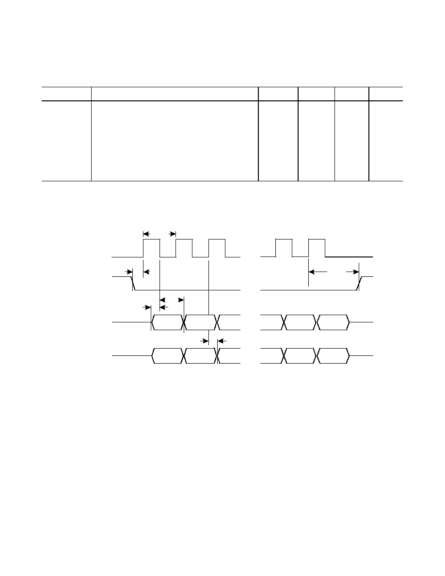
Preliminary Technical Information
AD6426
This Information applies to a product under development. Its characteristics and specifications are subject to change without notice. Analog Devices assumes no
obligation regarding future manufacture unless otherwise agreed to in writing. No responsibility is assumed by Analog Devices for its use; nor for any
infringements of patents or other rights of third parties which may result from its use. No license is granted by implication or otherwise under any patent or patent
rights of Analog Devices.
Revision Preliminary 2.3 (June 9, ´98)
- 39 -
Confidential Information
TIMING CHARACTERISTICS
EVBC Interface ASPORT
Parameter
Comment (see Figure 19)
Min
Typ
Max
Units
t
70
ASCLK period
384
ns
t
71
ASOFS setup time before ASCLK high
20
ns
t
72
ASOFS hold time after ASCLK high
20
ns
t
73
ASDI setup time before clock low
20
ns
t
74
ASDI hold time after clock low
20
ns
t
75
ASDO delay after clock high
0
20
ns
ASCLK (O)
ASDI (i)
ASDO (O)
t
70
D9 D8 D7 A2 A1 A0
ASOFS (O)
t
71
t
72
t
74
t
73
t
75
D9 D8 D7 A2 A1 A0
Figure 19. EVBC Interface ASPORT Timing
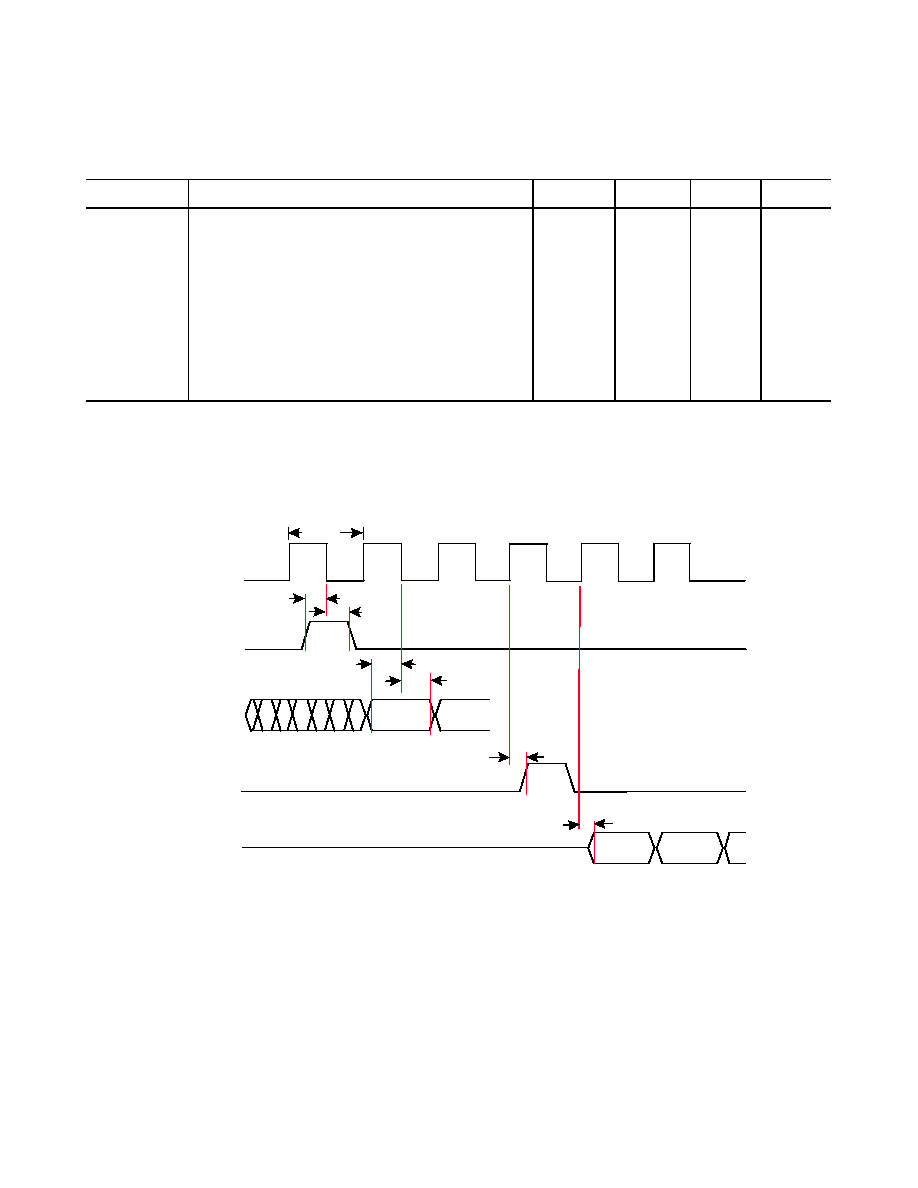
Preliminary Technical Information
AD6426
This Information applies to a product under development. Its characteristics and specifications are subject to change without notice. Analog Devices assumes no
obligation regarding future manufacture unless otherwise agreed to in writing. No responsibility is assumed by Analog Devices for its use; nor for any
infringements of patents or other rights of third parties which may result from its use. No license is granted by implication or otherwise under any patent or patent
rights of Analog Devices.
Revision Preliminary 2.3 (June 9, ´98)
- 40 -
Confidential Information
TIMING CHARACTERISTICS
EVBC Interface BSPORT
Parameter
Comment (see Figure 20)
Min
Typ
Max
Units
t
80
BSCLK period
76.9
ns
t
81
BSIFS setup time before BSCLK low
4
ns
t
82
BSIFS hold time after BSCLK low
7
ns
t
83
BSDI setup time before BSCLK low
4
ns
t
84
BSDI hold time after BSCLK low
7
ns
t
85
BSOFS delay after BSCLK high
15
ns
t
86
BSDO delay after BSCLK high
0
15
BSCLK (I)
BSDI (I)
BSDO (O)
t
80
D15 D14
BSIFS (I)
t
81
D15 D14
BSOFS (O)
t
82
t
83
t
84
t
85
t
86
Figure 20. EVBC Interface BSPORT Timing
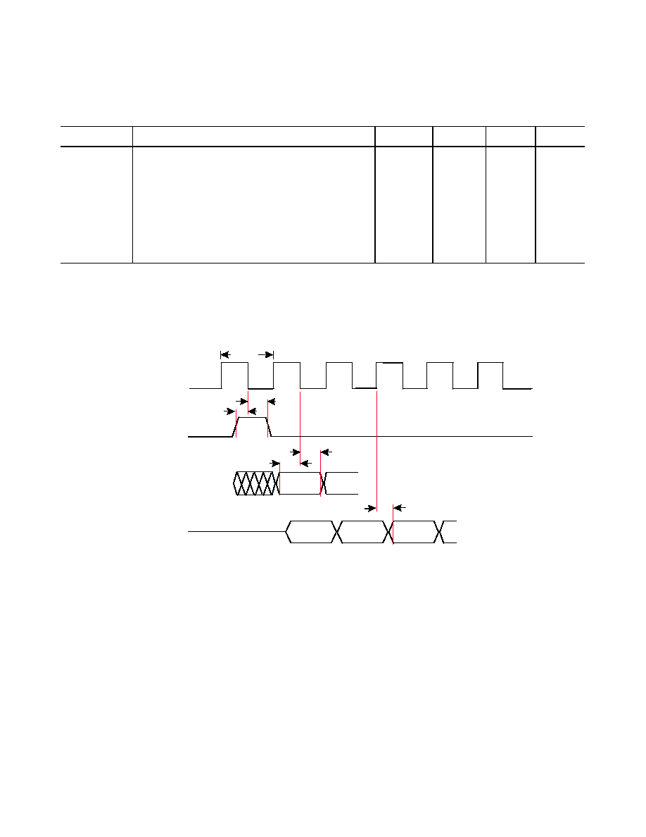
Preliminary Technical Information
AD6426
This Information applies to a product under development. Its characteristics and specifications are subject to change without notice. Analog Devices assumes no
obligation regarding future manufacture unless otherwise agreed to in writing. No responsibility is assumed by Analog Devices for its use; nor for any
infringements of patents or other rights of third parties which may result from its use. No license is granted by implication or otherwise under any patent or patent
rights of Analog Devices.
Revision Preliminary 2.3 (June 9, ´98)
- 41 -
Confidential Information
TIMING CHARACTERISTICS
EVBC Interface VSPORT
Parameter
Comment (see Figure 21)
Min
Typ
Max
Units
t
90
VSCLK period
76.9
ns
t
91
VSFS setup time before VSCLK low
4
ns
t
92
VSFS hold time after VSCLK low
7
ns
t
93
VSDI setup time before VSCLK low
4
ns
t
94
VSDI hold time after VSCLK low
7
ns
t
95
VSDO delay after VSCLK high
0
15
ns
VSCLK (I)
VSDI (I)
VSDO (O)
t
90
D15 D14
VSFS (I)
t
91
t
92
t
93
t
94
t
95
D15 D14 D13
Figure 21. EVBC Interface VSPORT Timing
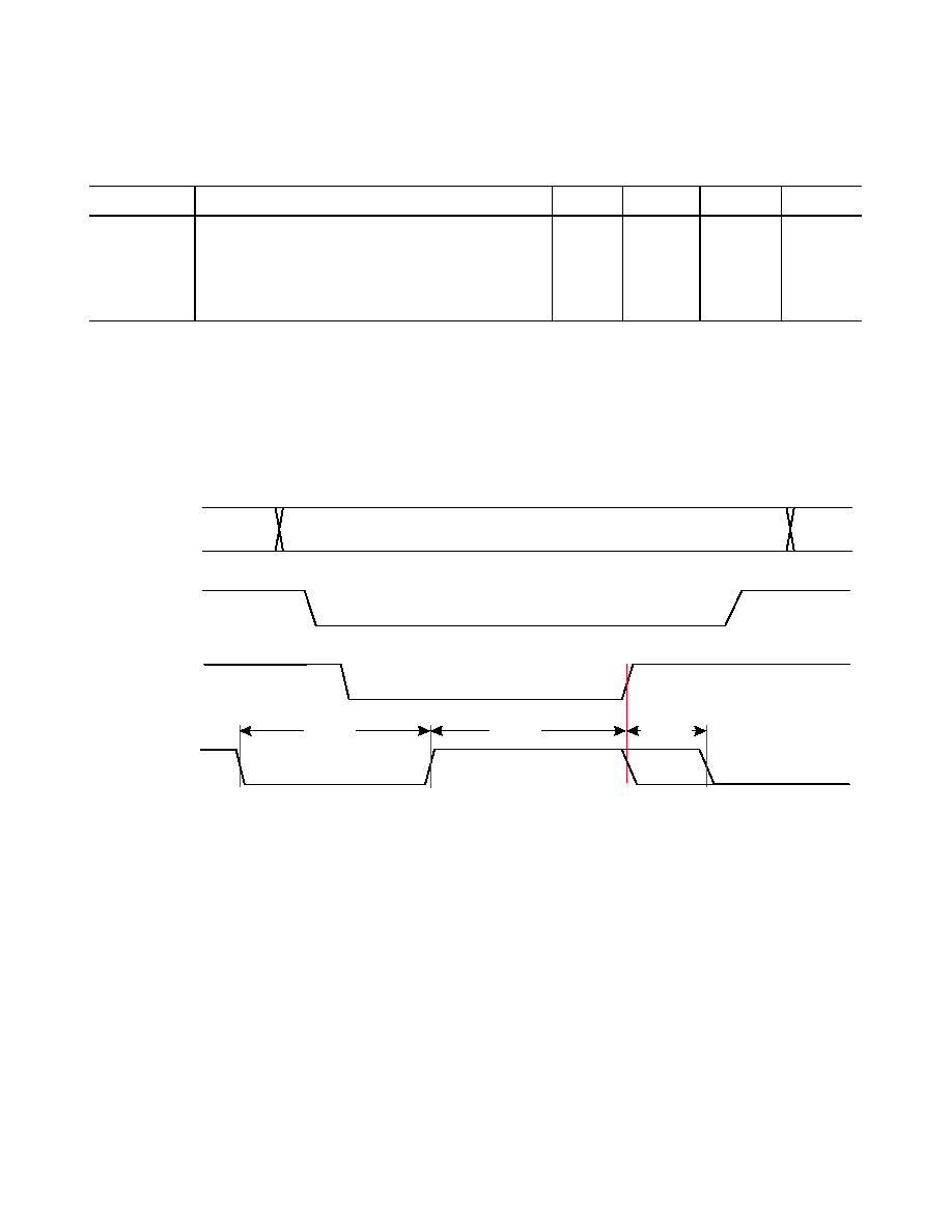
Preliminary Technical Information
AD6426
This Information applies to a product under development. Its characteristics and specifications are subject to change without notice. Analog Devices assumes no
obligation regarding future manufacture unless otherwise agreed to in writing. No responsibility is assumed by Analog Devices for its use; nor for any
infringements of patents or other rights of third parties which may result from its use. No license is granted by implication or otherwise under any patent or patent
rights of Analog Devices.
Revision Preliminary 2.3 (June 9, ´98)
- 42 -
Confidential Information
TIMING CHARACTERISTICS
Parallel Display Interface
Parameter
Comments (see Figure 22)
Min
Typ
Max
Units
t
100
LCD Control low width (6 CLKIN cycles)
462
ns
t
101
LCD Control high width (6 CLKIN cycles)
462
ns
t
102
LCD Control high width read extension (1 CLKIN
cycle)
77
ns
ADD 19:O
RD or HWR
LCDCTL
DISPLAYCS
t
100
t
101
t
102
Figure 22. Parallel Display Interface Timing
Preliminary Technical Information
AD6426
This Information applies to a product under development. Its characteristics and specifications are subject to change without notice. Analog Devices assumes no
obligation regarding future manufacture unless otherwise agreed to in writing. No responsibility is assumed by Analog Devices for its use; nor for any
infringements of patents or other rights of third parties which may result from its use. No license is granted by implication or otherwise under any patent or patent
rights of Analog Devices.
Revision Preliminary 2.3 (June 9, ´98)
- 43 -
Confidential Information
TIMING CHARACTERISTICS
Serial Display Interface
Parameter
Comment (see Figure 23)
Min
Typ
Max
Units
t
103
DISP_CLK Period
t
1
*8
or
t
1
*16
ns
t
104
DISP_CS Low to Data Valid
0.25 *t
103
+ 5
ns
t
105
DISP_CLK Low to Data Valid
5
ns
t
106
DISP_CLK Low to DISP_CS high
0.25 *t
103
ns
t
107
Data Valid to DISP_CLK High
0.25 *t
103
- 5
ns
//
DISP_CLK
//
//
D7
D6
D0
DISP_D0
DISP_CS
DISP_A0
t
103
t
107
t
105
t
104
t
106
Figure 23. Serial Display Interface

Preliminary Technical Information
AD6426
This Information applies to a product under development. Its characteristics and specifications are subject to change without notice. Analog Devices assumes no
obligation regarding future manufacture unless otherwise agreed to in writing. No responsibility is assumed by Analog Devices for its use; nor for any
infringements of patents or other rights of third parties which may result from its use. No license is granted by implication or otherwise under any patent or patent
rights of Analog Devices.
Revision Preliminary 2.3 (June 9, ´98)
- 44 -
Confidential Information
PACKAGING
LQFP Pin Locations
#
Pin Name
#
Pin Name
#
Pin Name
#
Pin Name
1
USCRI (MONCLK)
37
DATA12
73
TDI
109
AGCB
2
USCRX (MONRX)
38
DATA11
74
JTAGEN
110
TXPA
3
USCTX (MONTX)
39
DATA10
75
EEPROMEN
111
CALIBRATERADIO
4
USCCTS (ADD20)
40
DATA9
76
EEPROMCLK
112
RADIOPWRCTL
5
USCRTS (GPIO9)
41
DATA8
77
EEPROMDATA
113
TXENABLE
6
GPO10 (GPIO8)
42
RD
78
GND
114
GND
7
ADD19
43
GND
79
VDD
115
CLKIN
8
ADD18
44
VDD
80
VSDO
116
VDD
9
ADD17
45
UBS (HWR)
81
VSFS
117
GPIO7
10
ADD16
46
LBS (LWR)
82
VSDI
118
GPIO6
11
ADD15
47
DATA7
83
VSCLK
119
GPIO5
12
ADD14
48
DATA6
84
VBCRESET
120
GPIO4
13
ADD13
49
DATA5
85
RXON
121
GPIO3
14
ADD12
50
DATA4
86
CLKOUT
122
LCDCTL
15
ADD11
51
DATA3
87
BSDO
123
DISPLAYCS
16
GND
52
DATA2
88
BSOFS
124
BACKLIGHT
17
VDD
53
DATA1
89
BSIFS
125
VDD
18
ADD10
54
DATA0
90
BSDI
126
GND
19
ADD9
55
GND
91
BSCLK
127
OSC13MON (GPPWRCTL)
20
BOOTCODE (GND)
56
VDD
92
ASCLK
128
GPCS
21
ADD8
57
FLASHPWD
93
ASDI
129
KEYPADCOL3
22
ADD7
58
WR (GPIO2)
94
ASOFS
130
KEYPADCOL2
23
ADD6
59
GND
95
ASDO
131
KEYPADCOL1
24
ADD5
60
VDD
96
TXPHASE
132
KEYPADCOL0
25
ADD4
61
GPIO1
97
GPIO2 (CPPWD)
133
GND
26
ADD3
62
GPIO0
98
VDD (GND)
134
KEYPADROW5
27
ADD2
63
SIMSUPPLY
99
GND (VDD)
135
KEYPADROW4
28
ADD1
64
SIMPROG
100
OSCIN (SAMCS)
136
KEYPADROW3
29
ADD0
65
SIMRESET
101
OSCOUT (CPFS)
137
KEYPADROW2
30
RAMCS
66
SIMDATAIP
102
VDDRTC (CPDO)
138
KEYPADROW1
31
GND
67
SIMDATAOP
103
PWRON (CPDI)
139
KEYPADROW0
32
VDD
68
SIMCLK
104
SYNTHEN1
140
VDD
33
ROMCS
69
SIMCARD
105
SYNTHEN0
141
RESET
34
DATA15
70
TCK
106
SYNTHDATA
142
IRQ6
35
DATA14
71
TMS
107
SYNTHCLK
143
GPIO8 (BOOTCODE)
36
DATA13
72
TDO
108
AGCA
144
GPIO9 (H8MODE)
Note: pin names in ( ) are the AD6422 pin names from the AD20msp415 chipset.

Preliminary Technical Information
AD6426
This Information applies to a product under development. Its characteristics and specifications are subject to change without notice. Analog Devices assumes no
obligation regarding future manufacture unless otherwise agreed to in writing. No responsibility is assumed by Analog Devices for its use; nor for any
infringements of patents or other rights of third parties which may result from its use. No license is granted by implication or otherwise under any patent or patent
rights of Analog Devices.
Revision Preliminary 2.3 (June 9, ´98)
- 45 -
Confidential Information
PBGA Pin Locations
#
Pin Name
#
Pin Name
#
Pin Name
#
Pin Name
A1
USCR1
D1
ADD16
G1
BOOTCODE
K1
GND
A2
IRQ6
D2
ADD17
G2
ADD7
K2
ROMCS
A3
KEYPADROW0
D3
USCCTS
G3
ADD9
K3
DATA10
A4
KEYPADROW4
D4
GPIO8
G4
ADD4
K4
DATA9
A5
KEYPADCOL1
D5
VDD
G5
ADD1
K5
VDD
A6
GPCS
D6
GND
G6
ADD11
K6
DATA6
A7
VDD
D7
BACKLIGHT
G7
DATA3
K7
GND
A8
VDD
D8
GPIO5
G8
ASDI
K8
VDD
A9
CLKIN
D9
SYNTHCLK
G9
BSOFS
K9
SIMRESET
A10 GND
D10
PWRON
G10
VBCRESET
K10
EEPROMEN
A11 TXPA
D11
OSCOUT
G11
BSDI
K11
EEPROMDATA
A12 AGCB
D12
VDD
G12
BSIFS
K12
GND
B1
USCRX
E1
ADD13
H1
ADD6
L1
DATA15
B2
GPIO9
E2
ADD12
H2
ADD3
L2
DATA13
B3
RESET
E3
ADD18
H3
ADD5
L3
DATA8
B4
KEYPADROW1
E4
ADD15
H4
VDD
L4
UBS
B5
KEYPADROW5
E5
ADD19
H5
GND
L5
DATA4
B6
KEYPADCOL2
E6
KEYPADROW3
H6
FLASHPWD
L6
DATA0
B7
GND
E7
KEYPADCOL3
H7
SIMPROG
L7
WR
B8
GPIO3
E8
LCDCTL
H8
VDD
L8
GPIO0
B9
GPIO7
E9
SYNTHEN1
H9
VSCLK
L9
SIMDATAIP
B10 TXENABLE
E10
TXPHASE
H10
VSDO
L10
SIMCARD
B11 AGCA
E11
GND
H11
CLKOUT
L11
TDO
B12 SYNTHDATA
E12
ASDO
H12
RXON
L12
JTAGEN
C1
GPIO10
F1
VDD
J1
ADD2
M1
DATA12
C2
USCRTS
F2
ADD10
J2
RAMCS
M2
DATA11
C3
USCTX
F3
ADD14
J3
ADD0
M3
RD
C4
KEYPADROW2
F4
GND
J4
DATA14
M4
LWR
C5
KEYPADCOL0
F5
ADD8
J5
DATA7
M5
DATA5
C6
OSC13MON
F6
DISPLAYCS
J6
DATA2
M6
DATA1
C7
GPIO4
F7
BSDO
J7
GPIO1
M7
VDD
C8
GPIO6
F8
VDDRTC
J8
SIMCLK
M8
GND
C9
RADIOPWRCTL
F9
GPIO2
J9
TMS
M9
SIMSUPPLY
C10 CALIBRATERADIO
F10
BSCLK
J10
EEPROMCLK
M10
SIMDATAOP
C11 SYNTHEN0
F11
ASOFS
J11
VSFS
M11
TCK
C12 OSCIN
F12
ASCLK
J12
VSDI
M12
TDI
Preliminary Technical Information
AD6426
This Information applies to a product under development. Its characteristics and specifications are subject to change without notice. Analog Devices assumes no
obligation regarding future manufacture unless otherwise agreed to in writing. No responsibility is assumed by Analog Devices for its use; nor for any
infringements of patents or other rights of third parties which may result from its use. No license is granted by implication or otherwise under any patent or patent
rights of Analog Devices.
Revision Preliminary 2.3 (June 9, ´98)
- 46 -
Confidential Information
AD6426
TOP VIEW
(PINS DOWN)
1
144
36
37
72
73
108
109
USCRI
USCRX
USCTX
USCCTS
USCRTS
GPIO10
ADD19
ADD18
ADD17
ADD16
ADD15
ADD14
ADD13
ADD12
ADD11
GND
VDD
ADD10
ADD9
BOOTCODE
ADD8
ADD7
ADD6
ADD5
ADD4
ADD3
ADD2
ADD1
ADD0
RAMCS
GND
VDD
ROMCS
DATA15
DATA14
DATA13
DATA12
DATA11
DATA10
DATA9
DATA8
RD
GND
VDD
UBS
LBS
DATA7
DATA6
DATA5
DATA4
DATA3
DATA2
DATA1
DATA0
GND
VDD
FLASHPWD
WR
GND
VDD
GPIO1
GPIO0
SIMSUPPLY
SIMPROG
SIMRESET
SIMDATAIP
SIMDATAOP
SIMCLK
SIMCARD
TCK
TMS
TDO
AGCA
SYNTHCLK
SYNTHDATA
SYNTHEN0
SYNTHEN1
PWRON
VDDRTC
OSCOUT
OSCIN
GND
VDD
GPIO2
TXPHASE
ASDO
ASOFS
ASDI
ASCLK
BSCLK
BSDI
BSIFS
BSOFS
BSDO
CLKOUT
RXON
VBCRESET
VSCLK
VSDI
VSFS
VSDO
VDD
GND
EEPROMDATA
EEPROMCLK
EEPROMEN
JTAGEN
TDI
GPIO9
GPIO8
IRQ6
RESET
VDD
KEYPADROW0
KEYPADROW1
KEYPADROW2
KEYPADROW3
KEYPADROW4
KEYPADROW5
GND
KEYPADCOL0
KEYPADCOL1
KEYPADCOL2
KEYPADCOL3
GPCS
OSC13MON
GND
VDD
BACKLIGHT
DISPLAYCS
LCDCTL
GPIO3
GPIO4
GPIO5
GPIO6
GPIO7
VDD
CLKIN
GND
TXENABLE
RADIOPWRCTL
CALIBRATERADIO
TXPA
AGCB
Figure 24: LQFP Pin Locations
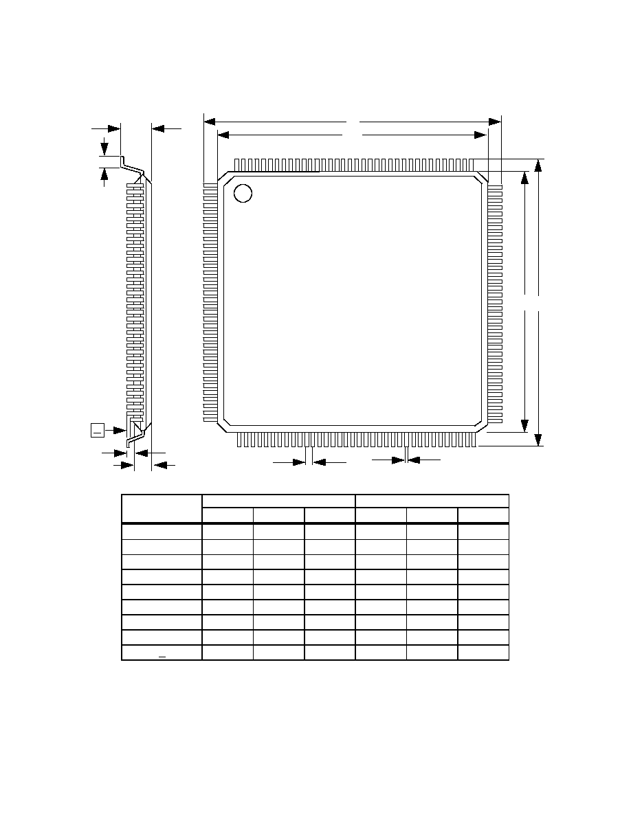
Preliminary Technical Information
AD6426
This Information applies to a product under development. Its characteristics and specifications are subject to change without notice. Analog Devices assumes no
obligation regarding future manufacture unless otherwise agreed to in writing. No responsibility is assumed by Analog Devices for its use; nor for any
infringements of patents or other rights of third parties which may result from its use. No license is granted by implication or otherwise under any patent or patent
rights of Analog Devices.
Revision Preliminary 2.3 (June 9, ´98)
- 47 -
Confidential Information
LQFP Outline Dimensions
D
D
1
E
E
1
TQFP 144
TOP VIEW
(PINS DOWN)
B
e
1
144
36
37
A
L
A
1
A
2
72
73
108
109
MILLIMETERS
INCHES
DIM
MIN
TYP
MAX
MIN
TYP
MAX
A
1.60
0.063
A
1
0.05
0.15
0.002
0.006
A
2
1.35
1.40
1.45
0.053
0.055
0.057
D, E
21.80
22.00
22.20
0.858
0.866
0.874
D
1
, E
1
19.90
20.00
20.10
0.783
0.787
0.791
L
0.5
0.6
0.75
0.019
0.024
0.030
e
0.50
0.020
B
0.17
0.22
0.27
0.007
0.009
0.011
Ç
0.08
0.003
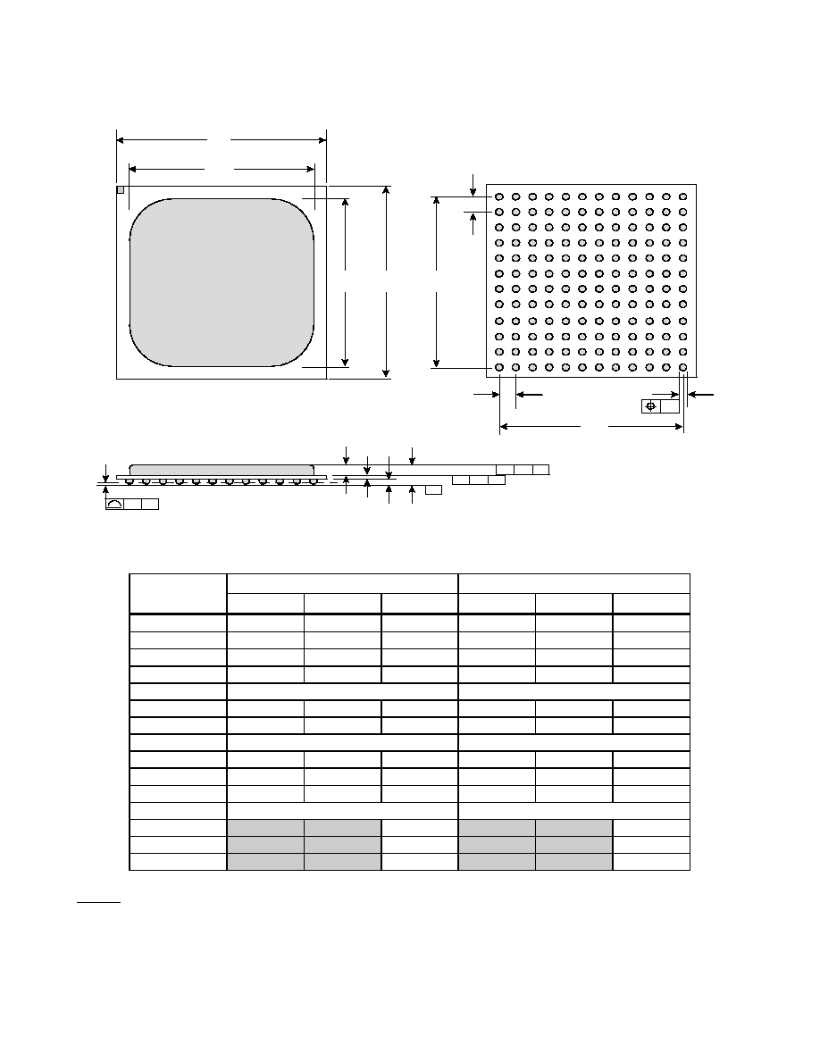
Preliminary Technical Information
AD6426
This Information applies to a product under development. Its characteristics and specifications are subject to change without notice. Analog Devices assumes no
obligation regarding future manufacture unless otherwise agreed to in writing. No responsibility is assumed by Analog Devices for its use; nor for any
infringements of patents or other rights of third parties which may result from its use. No license is granted by implication or otherwise under any patent or patent
rights of Analog Devices.
Revision Preliminary 2.3 (June 9, ´98)
- 48 -
Confidential Information
PBGA Outline Dimensions
A
B
C
D
E
F
G
H
1
2
3
4
5
6
7
8
9
10
11
12
J
K
L
M
e
D2
D
E2
E
e
E1
D1
b
0.10
A2 c
A1 A
//
ccc C
-C-
//
ccc C
aaa C
AD6426
TOP VIEW
(Pins Down)
MILLIMETERS
INCHES
DIM
MIN
TYP
MAX
MIN
TYP
MAX
A
1.42
1.65
1.80
0.05591
0.06496
0.07087
A1
0.30
0.40
0.50
0.01181
0.01575
0.01968
A2
0.75
0.90
0.97
0.02953
0.03543
0.03819
D
12.85
13.00
13.15
0.50590
0.51181
0.51772
D1
11.00 BSC
0.43307 BSC
D2
9.95
10.75
11.55
0.39173
0.42323
0.45472
E
12.85
13.00
13.15
0.50591
0.51181
0.51772
E1
11.00 BSC
0.43307 BSC
E2
9.95
10.75
11.55
0.39173
0.42323
0.45472
b
0.45
0.55
0.65
0.17716
0.02165
0.02559
c
0.27
0.35
0.43
0.01063
0.01378
0.01693
e
1.00 BSC
0.03937 BSC
aaa
0.15
0.00591
bbb
0.20
0.00787
ccc
0.25
0.00984
NOTE:
1. BSC - Between Spacing Centers

AD6426 Data Sheet Change Summary
June 10, 1998
Page
1 of 2
AD6426 Preliminary Revision 2.3
(Changes from Revision 1.0)
Number
Date
Description of Change
1
5/19/98
Motorola Serial Display mode added.
2
5/19/98
TXENABLE NMI function freeing up the IRQ6 pin added.
3
5/19/98
Dimensional tolerances for BGA package outline drawing added.
4
5/19/98
Memory I/F timing specs separated into characteristics and requirements.
5
5/19/98
Dual band control signals renamed- BANDSELECT0 is multiplexed with GPIO[2], BANDSELECT1
is multiplexed with GPIO[1]. For DB radios requiring a single Bandselect bit, BANDSELECT0 is
enabled. For DB radios requiring 2 Bandselect bits then both BANSELECT0,1 can be enabled.
These signals were previously referred to as BANDSELECT and DCSSEL.
6
5/19/98
VBC and radio I/F diagram in Figure 6 updated to show a generic DB radio I/F.
7
5/19/98
DAI I/F Pins updated to be consistent with DAI Box users manual.
8
5/19/98
GPIO[7:0] Pin functions in Mode D (Table 24) were incorrectly listed as being all Tristate outputs.
The correct function is GPIO7 = TRI and GPIO[6:0] = O.
9
5/20/98
Requirements for 32kHz crystal for slow clocking added.
10
5/20/98
Pin functions in Emulation mode GPO 0,6,7 in Table 24 are renamed to reserve.
11
5/20/98
Memory Interface Timing Specification: read timing specs changed to max with the exception of
Control Processor data hold and Parameters broken out separately into requirements and
characteristics.
12
6/9/98
In Fig 24 the following pins were incorrectly labeled and thus changed;
a) Pin 45 from HWR to UBS
b) Pin 46 from LWR to LBS
c) Pin 98 from GND to VDD
d) Pin 99 from VDD to GND

AD6426 Data Sheet Change Summary
June 10, 1998
Page
2 of 2
AD6426 Preliminary Revision 1.0
(Changes from Revision 0.1)
Number
Date
Description of Change
1
1/15/98
Dallas I/F added to Feature list.
2
1/15/98
Dallas I/F enable bit polarity changed from logic 1 to 0.
3
1/15/98
Dual Band control section added describing BANDSELECT and DCSSEL signals.
4
1/15/96
Serial Display Interface Timing Characteristics and Diagram added as Figure 23.
5
1/15/98
General Description: F7.2 data services deleted, this is not supported on the EGSMP.
6
1/15/98
General Description: AD6421/25 interfaces to the EGSMP.
7
1/15/98
Serial Display Reset signal removed from Figure 2.
Display driver chip reset input is connected to the AD6425 VBC Reset Input and both are driven by
the AD6426 VBC reset output.
8
1/15/98
Pin Functionality: VBCRESET added note, also used for Display Reset.
9
1/15/98
Pin Functionality: GPIO1 added note, alternate function DCS_ON.
10
1/15/98
CC Control Registers: Interrupt counter (Addr. 48) changed from 7 to 8 bits.
11
1/15/98
SIM Interface timing characteristics deleted - SIM signals are completely asynchronous with respect
to SIMCLK.
12
1/15/98
Plastic Ball Grid Array (PBGA) Package pinout and outline drawing added.
13
2/16/98
EVBC and radio Interface block diagram in Figure 6 updated with dual band control signals.
14
2/16/98
V
CLKIN
, Clock Input Voltage for ac-coupled sine wave input changed from 100 mV
PP
to 250 mV
PP.
15
2/16/98
Added scan registers USCRX (O), USCRXEN (B), and VSDOEN (T)
Corrected output polarity in Notes to active-low (0=output).
16
2/16/98
Added H8 Control registers and register contents in Tables 3 and 4.
17
2/16/98
Buffered UART Register Contents added in Table 5.
18
2/26/98
I
IH
, I
IL
Input Current spec min -10, max 10
µ
A added.
19
2/26/98
I
IH
, I
IL
Input Current spec min -10, max 10
µ
A added.
20
2/26/98
I
OZL
, Low Level Output 3-State Leakage Current min 10, max 10
µ
A I
OZH
, High Level Output 3-State
Leakage Current min 10, max 10
µ
A.
21
2/26/98
Absolute Max ratings broken out separately for PBGA package.
22
2/26/98
Control Processor Data setup time changed from 10 to 68 ns.
23
2/26/98
Radio interface section: a reference to the TTP/Hitachi radios added "AD6426 Radio Interface
supports radio architectures based on Siemens, Philips, and TTP/Hitachi RF chipsets".
24
2/27/98
Pin Functionality: OSC13MON pin moved from RTC section to general section.
25
2/27/98
Memory interface timing diagram replaced with one used in 6422 data sheet.
26
2/27/98
CC register 46 bits 4-7 SIMCLOCK Polarity, SIMCLOCK off. SIMCLOCK Control, STBYCLKON
removed no longer used on 6426.
27
3/9/98
CC registers 80-87 slow clocking control removed from Table 1 & 2 per TTP's request.
28
3/9/98
Peripheral registers 83, 106-109 removed from Table 3 & 4 per TTP's request.
29
3/9/98
All Buffered UART registers removed per TTP's request.
Document Outline
- Change Summary
- GENERAL DESCRIPTION
- FEATURES
- Figure 1. Functional Block Diagram
- ORDERING GUIDE
- Figure 2. External Interfaces of the AD6426
- Table of Contents
- PIN FUNCTIONALITY ( Normal Mode)
- Pin.. Page 2
- Pin.. Page 3
- OVERVIEW
- FUNCTIONAL PARTITIONING
- Channel Codec Sub-System
- Figure 3. Channel Codec Subsystem
- Processor Sub-System
- DSP Sub-System
- Speech Transcoding
- Equalization
- Audio Control
- Tone Generation
- Automatic Frequency Control (AFC)
- Automatic Gain Control (AGC)
- REGISTERS
- Table 1. CC Control Registers
- Table 2. CC Control Register Contents
- Table 3. H8 Peripheral Control Registers
- Table 4. H8 Peripheral Register Contents
- Table 4. Pg. 2
- GENERAL CONTROL
- Clocks
- Slow Clocking
- Real Time Clock and Alarm
- Reset
- Interrupts
- NMI
- Wait
- Automatic Booting
- Power Control
- INTERFACES
- Memory Interface
- Table 5. Memory Interface
- EEPROM Interface
- Table 6. EEPROM Interface
- SIM Interface
- Accessory Interface
- Table 8. Accessory Interface
- Table 9. Additional GPIO / GPO Pins
- Universal System Connector Interface
- Operating modes of the USC
- Buffered UART Mode (Booting/Data Services)
- Time-shared Mode (Multi-switch)
- DAI Acoustic Mode Testing
- IQ Monitoring
- 16 bit Mode
- Keypad / Backlight / Display Interface
- Table 10. Keypad / Backlight / Display Interface
- Table 11. Backlight Frequency
- Figure 5. Parallel Display Interface
- Serial Display Interface
- Display Reset
- Battery ID Interface
- EVBC Interface
- Table 12. EVBC Interface
- Figure 6. EVBC and Radio Interface
- Radio Interface
- Dual Band Control
- Generic Pins
- RADIOPWRCTL
- Table 13. Radio Interface
- GPIO6 - VBIAS
- GPIO7 - ANTENNASELECT
- Tx Timing Control
- Rx Timing Control
- RXON
- CALIBRATERADIO
- Figure 8. Autocalibration
- Synthesizer Control
- SYNTHEN0 : 1
- SYNTHDATA and SYNTHCLK
- Table 14. Pin Mode
- Table 15. Pin Function in Mode 1
- Table 16. Pin Function in Modes 2 and 3
- AGC Control
- Table 17. Pin Function in Mode 1
- Table 18. Pin Function in Mode 2
- Table 19. Pin Function in Mode 3
- Figure 9. OCE Signal
- TEST INTERFACE
- Table 20. Test Interface
- JTAG Port
- Figure 10. JTAG Registers
- Table 21. JTAG Instructions
- ExTest Instruction
- Clamp Instruction
- Sample/Preload Instruction
- Boundary Register
- Table 22. Boundary Scan Path
- DoBist Instruction
- Mode D Instruction
- Reset
- Debug Port Interface
- MODES OF OPERATION
- Table 23. Modes of Operation
- Normal Mode (Mode A)
- Emulation Mode (Mode D)
- Table 24. Pin Functions in Mode D
- FEATURE MODES
- DAI Mode
- High Speed Logging
- Table 26. HSL Mode
- Table 27. Mapping of HSL Port Nibbles
- Figure 11. HSL Timing
- SPECIFICATIONS
- General
- ABSOLUTE MAXIMUM RATINGS
- LQFP Package
- PBGA Package
- TIMING CHARACTERISTICS
- Clocks
- Figure 12. Load Circuit for Timing Specifications
- Figure 13. Clock Input
- Figure 14. Clock Output
- TIMING SPECIFICATION
- Memory Interface
- Figure 15. Memory Interface Timing
- Radio Interface
- Figure 16. Synthesizer Interface Timing
- High Speed Logging Interface
- Figure 17. High Speed Logging Interface
- Data Interface
- Figure 18: Data Interface Timing
- Test Interface
- EVBC Interface ASPORT
- Figure 19. EVBC Interface ASPORT Timing
- EVBC Interface BSPORT
- Figure 20. EVBC Interface BSPORT Timing
- EVBC Interface VSPORT
- Figure 21. EVBC Interface VSPORT Timing
- Parallel Display Interface
- Figure 22. Parallel Display Interface Timing
- Serial Display Interface
- Figure 23. Serial Display Interface
- PACKAGING
- LQFP Pin Locations
- PBGA Pin Locations
- Figure 24: LQFP Pin Locations
- LQFP Outline Dimensions
- PBGA Outline Dimensions