/home/web/htmldatasheet/RUSSIAN/html/ad/164252
REV. 0
Information furnished by Analog Devices is believed to be accurate and
reliable. However, no responsibility is assumed by Analog Devices for its
use, nor for any infringements of patents or other rights of third parties
which may result from its use. No license is granted by implication or
otherwise under any patent or patent rights of Analog Devices.
a
AD6622
One Technology Way, P.O. Box 9106, Norwood, MA 02062-9106, U.S.A.
Tel: 781/329-4700
World Wide Web Site: http://www.analog.com
Fax: 781/326-8703
© Analog Devices, Inc., 2000
Four-Channel, 75 MSPS Digital
Transmit Signal Processor (TSP)
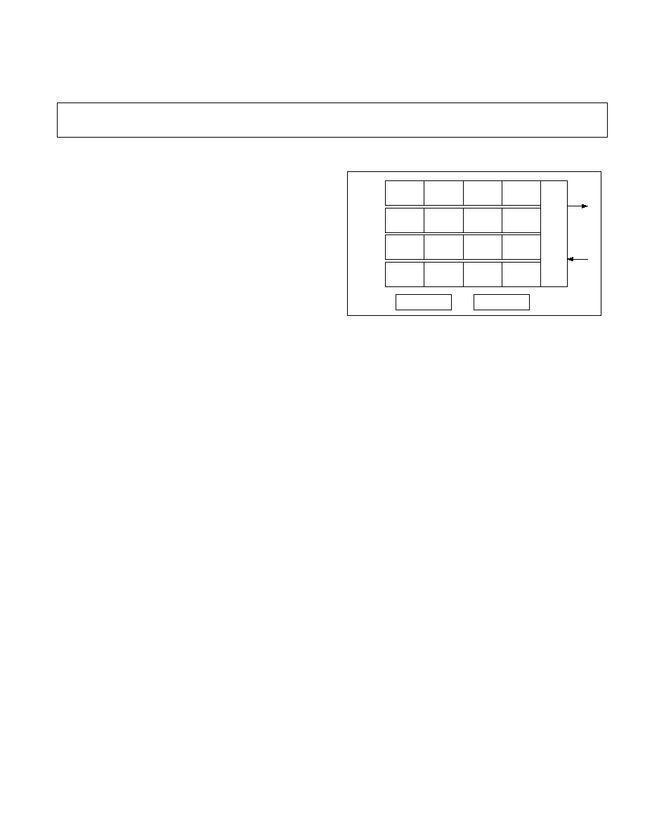
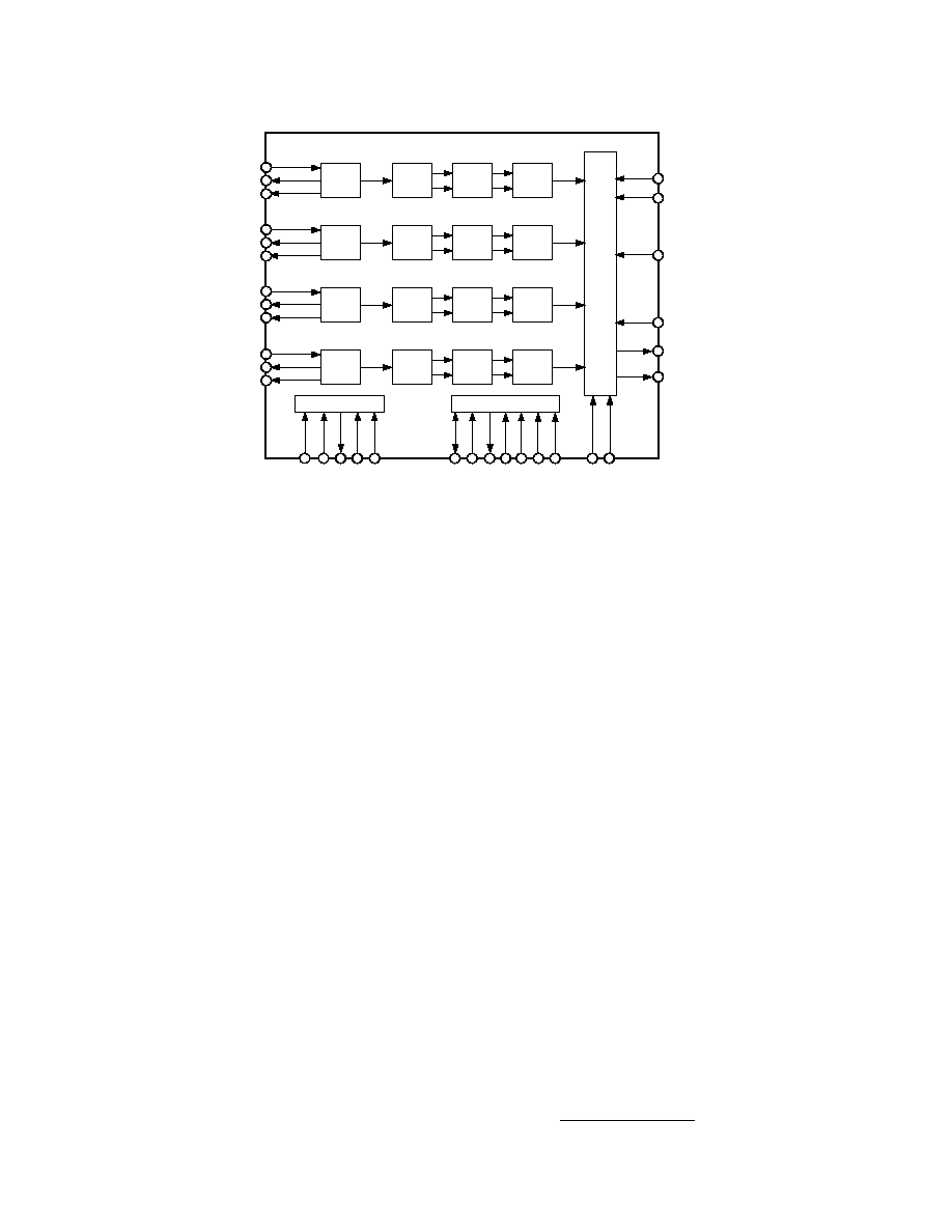
FUNCTIONAL BLOCK DIAGRAM
CH A
CH B
CH C
CH D
RCF
NCO
18
18
PORT
CIC
FILTER
SPORT
SPORT
SPORT
SPORT
RCF
RCF
RCF
CIC
FILTER
CIC
FILTER
CIC
FILTER
NCO
NCO
NCO
JTAG
SUMMATION
FEATURES
Wideband Digital IF Parallel Output
Wideband Digital IF Parallel Input
Allows Cascade of Chips for Additional Channels
Programmable IF and Modulation for Each Channel
Programmable Interpolating RAM Coefficient Filter
High-Speed CIC Interpolating Filter
NCO Frequency Translation
Worst Spur Better than 100 dBc
Tuning Resolution Better than 0.02 Hz
Real or Complex Outputs
Digital Summation of Channels
Clipped or Wrapped Overrange
Two's Complement or Offset Binary Output
Separate 3-Wire Serial Data Input for Each Channel
Microprocessor Control
JTAG Boundary Scan
APPLICATIONS
Cellular/PCS Base Stations
Micro/Pico Cell Base Stations
WBCDMA
Wireless Local Loop Base Stations
Phase Array Beam Forming Antennas
PRODUCT DESCRIPTION
The AD6622 comprises four identical digital Transmit Signal
Processors (TSPs) complete with synchronization circuitry and
cascadable wideband channel summation. An external digital-
to-analog converter (DAC) is all that is required to complete a
wide band digital up-converter. On-chip tuners allow the relative
phase and frequency for each RF carrier to be independently
controlled.
Each TSP has three cascaded signal processing elements: a
RAM-programmable Coefficient interpolating Filter (RCF), a
programmable Cascaded Integrator Comb (CIC) interpolating
filter, and a Numerically Controlled Oscillator/tuner (NCO).
The outputs of the four TSPs are summed and scaled on-chip.
In multichannel wideband transmitters, multiple AD6622s may
be combined using the chip's cascadable output summation stage.
Each channel provides independent serial data inputs that may
be directly connected to the serial port of DSP chips. User pro-
grammable FIR filters can be used to filter linear inputs.
All control registers and coefficient values are programmed through
a generic microprocessor interface. Two microprocessor bus
modes are supported. All inputs and outputs are LVCMOS
compatible. All outputs are LVCMOS and 5 V TTL compatible.

2
REV. 0
AD6622SPECIFICATIONS
RECOMMENDED OPERATING CONDITIONS
Test
AD6622AS
Parameter
Level
Min
Typ
Max
Unit
VDD
IV
2.4
3.0
3.3
V
T
AMBIENT
IV
40
+25
+70
°C
ELECTRICAL CHARACTERISTICS
Test
AD6622AS
Parameter (Conditions)
Temp
Level
Min
Typ
Max
Unit
LOGIC INPUTS (5 V TOLERANT)
3.0 V CMOS
Logic Compatibility
Full
Logic "1" Voltage
Full
IV
2.0
VDD + 0.3
V
Logic "0" Voltage
Full
IV
0.3
+0.8
V
Logic "1" Current
Full
IV
1
10
µA
Logic "0" Current
Full
IV
1
10
µA
Input Capacitance
25
°C
V
4
pF
LOGIC OUTPUTS
Logic Compatibility
Full
Logic "1" Voltage (I
OH
= 0.25 mA)
Full
IV
VDD 0.05
VDD 0.035
V
Logic "0" Voltage (I
OL
= 0.25 mA)
Full
IV
0.02
0.05
V
IDD SUPPLY CURRENT
CLK = 60 MHz, 3.3 V
1
Full
IV
506
566
1
mA
CLK = GSM Example
V
297
2
mA
CLK = IS-136 Example
V
240
2
mA
CLK = WBCDMA Example
V
209
2
mA
Sleep Mode
Full
IV
0.1
0.5
mA
POWER DISSIPATION
CLK = 60 MHz, 3.3 V
1
Full
IV
1.77
1.87
W
CLK = GSM Example
V
0.89
2
W
CLK = IS-136 Example
V
0.72
2
W
CLK = WBCDMA Example
V
0.627
2
W
Sleep Mode
Full
IV
0.33
1.65
mW
NOTES
1
This specification denotes an absolute maximum supply current for the device. The conditions include all channels active, minimum interpolation in both CIC stages,
maximum switching of input data, and maximum VDD of 3.3 V. In an actual application the power will be less; see the Thermal Management section of the data sheet
for further details.
2
GSM interpolation = 120 at 65 MHz, 4 channels active, IS-136 interpolation = 2560 at 62.208 MHz, 4 channels active. WBCDMA interpolation = 64, 4 channels
interleaved at 61.44 MHz.
Specifications subject to change without notice.

AD6622
3
REV. 0
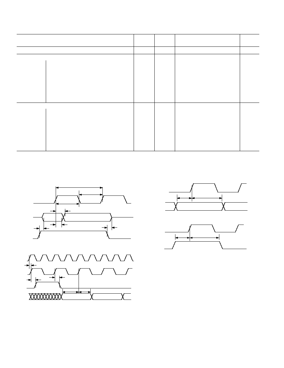
TIMING CHARACTERISTICS
1
Test
AD6622AS
Name
Parameter (Conditions)
Temp
Level
Min
Typ
Max
Unit
CLK Timing Requirements:
t
CLK
CLK Period
Full
IV
13.3
ns
t
CLKL
CLK Width Low
Full
IV
5.5
0.5
× t
CLK
ns
t
CLKH
CLK Width High
Full
IV
5.5
0.5
× t
CLK
ns
RESET Timing Requirements:
t
RESL
RESET Width Low
Full
IV
30.0
ns
Input Wideband Data Timing Requirements:
t
SI
Input to CLK Setup Time
Full
IV
0.5
ns
t
HI
Input to CLK Hold Time
Full
IV
3.5
ns
Parallel Output Switching Characteristics:
t
SO
CLK to Output Setup Time
Full
IV
12
ns
t
HO
CLK to Output Hold Time
Full
IV
4.1
ns
t
ZO
Output Three-State Time
Full
V
5
ns
SYNC Timing Requirements:
t
SS
SYNC to CLK Setup Time
Full
IV
2.6
ns
t
HS
SYNC to CLK Hold Time
Full
IV
1.5
ns
Serial Port Timing Requirements:
t
DSCLK
CLK to SCLK Delay
Full
V
8.5
ns
t
DSDFS
SCLK to SDFS Delay
Full
IV
1.2
+2.4
ns
t
SSI
SDI to SCLK Setup Time
Full
IV
8.5
ns
t
HSI
SDI to SCLK Hold Time
Full
IV
5.5
ns
t
SCS
Serial Clock Skew
Full
IV
7
ns
MICROPROCESSOR PORT, MODE INM (MODE = 0)
MODE INM Write Timing:
t
HWR
WR(R/W) to RDY(DTACK) Hold Time
Full
IV
0
ns
t
SAM
Address/Data to
WR(R/W) Setup Time
Full
IV
0
ns
t
HAM
Address/Data to RDY(
DTACK) Hold Time
Full
IV
0
ns
t
DRDY
WR(R/W) to RDY(DTACK) Delay
Full
IV
10.2
ns
t
ACC
FAST
WR(R/W) to RDY(DTACK) High Delay
Full
IV
2
× t
CLK
3
× t
CLK
ns
t
ACC
MEDIUM
WR(R/W) to RDY(DTACK) High Delay
Full
IV
3
× t
CLK
4
× t
CLK
ns
t
ACC
SLOW
WR(R/W) to RDY(DTACK) High Delay
Full
IV
4
× t
CLK
5
× t
CLK
ns
MODE INM Read Timing:
t
SAM
Address to
RD(DS) Setup Time
Full
IV
0
ns
t
HA
Address to Data Hold Time
Full
IV
0
ns
t
ZD
Data Three-State Delay
Full
IV
3.4
7
10.5
ns
t
DD
RDY(
DTACK) to Data Delay
Full
IV
t
CLK
10
ns
t
DRDY
RD(DS) to RDY(DTACK) Delay
Full
IV
10.2
ns
t
ACC
FAST
RD(DS) to RDY(DTACK) High Delay
Full
IV
2
× t
CLK
3
× t
CLK
ns
t
ACC
MEDIUM
RD(DS) to RDY(DTACK) High Delay
Full
IV
3
× t
CLK
4
× t
CLK
ns
t
ACC
SLOW
RD(DS) to RDY(DTACK) High Delay
Full
IV
4
× t
CLK
5
× t
CLK
ns
(C
LOAD
= 40 pF, all outputs unless specified)
AD6622
4
REV. 0
Test
AD6622AS
Name
Parameter (Conditions)
Temp
Level
Min
Typ
Max
Unit
MICROPROCESSOR PORT, MODE MNM (MODE = 1)
MODE MNM Write Timing:
t
HDS
DS(RD) to DTACK(RDY) Hold Time
Full
IV
0
ns
t
HRW
R/
W(WR) to DTACK(RDY) Hold Time
Full
IV
0
ns
t
SAM
Address/Data to R/
W(WR) Setup Time
Full
IV
0
ns
t
HAM
Address/Data to R/
W(WR) Hold Time
Full
IV
0
ns
t
DDTACK
DS(RD) to DTACK(RDY) Delay
Full
IV
1
× t
CLK
ns
t
ACC
FAST
R/
W(WR) to DTACK(RDY) Low Delay
Full
IV
2
× t
CLK
3
× t
CLK
ns
t
ACC
MEDIUM
R/
W(WR) to DTACK(RDY) Low Delay
Full
IV
3
× t
CLK
4
× t
CLK
ns
t
ACC
SLOW
R/
W(WR) to DTACK(RDY) Low Delay
Full
IV
4
× t
CLK
5
× t
CLK
ns
MODE MNM Read Timing:
t
SAM
Address to
DS(RD) Setup Time
Full
IV
0
ns
t
HA
Address to Data Hold Time
Full
IV
0
ns
t
ZD
Data Three-State Delay
Full
IV
0
ns
t
DD
DTACK(RDY) to Data Delay
Full
IV
t
CLK
10
ns
t
DDTACK
DS(RD) to DTACK(RDY) Delay
Full
IV
1
× t
CLK
ns
t
ACC
FAST
DS(RD) to DTACK(RDY) Low Delay
Full
IV
2
× t
CLK
3
× t
CLK
ns
t
ACC
MEDIUM
DS(RD) to DTACK(RDY) Low Delay
Full
IV
3
× t
CLK
4
× t
CLK
ns
t
ACC
SLOW
DS(RD) to DTACK(RDY) Low Delay
Full
IV
4
× t
CLK
5
× t
CLK
ns
NOTES
1
All Timing Specifications valid over VDD range of 2.4 V to 3.3 V.
Specifications subject to change without notice.
CLK
OUT[17:0],
QOUT
t
CLK
t
CLKL
t
CLKH
t
ZO
t
HO
t
ZO
OEN
t
SO
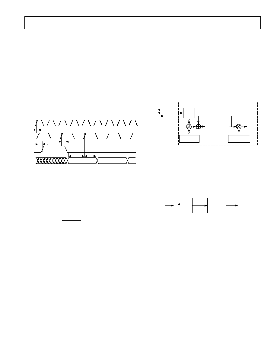
Figure 1. Parallel Output Switching Characteristics
CLK
SCLK
SDFS
SDI
CLKn
DATAn
t
DSCLK
t
DSDFS
t
DSDFS
t
SSI
t
HSI
Figure 2. Serial Port Switching Characteristics
CLK
IN[17:0],
QIN
t
SI
t
HI
Figure 3. Wideband Input Timing
SYNC
CLK
t
SS
t
HS
Figure 4. SYNC Timing Inputs
AD6622
5
REV. 0
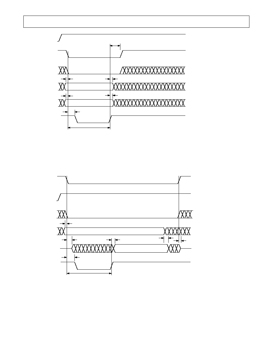
WR (R/W)
RD (DS)
CS
A[2:0]
D[7:0]
RDY
(
DTACK)
t
HWR
t
SAM
t
HAM
t
SAM
t
HAM
t
DRDY
t
ACC
VALID ADDRESS
VALID DATA
1. t
ACC
ACCESS TIME DEPENDS ON THE ADDRESS ACCESSED. ACCESS TIME IS MEASURED FROM THE FE OF
WR TO THE RE OF RDY.
2. t
ACC
FAST REQUIRES A MAXIMUM OF THREE CLK PERIODS AND APPLIES TO A[2:0] = 7, 6, 5, 3, 2, 1
3. t
ACC
MEDIUM REQUIRES A MAXIMUM OF FOUR CLK PERIODS AND APPLIES TO A[2:0] = 4 AND 0 IF THE ACCESS IS TO A CONTROL REGISTER
VERSUS A RAM REGISTER.
4. t
ACC
SLOW REQUIRES A MAXIMUM OF FIVE CLK PERIODS AND APPLIES TO A[2:0] = 0 WHEN ACCESSING RAM REGISTERS.
Figure 5. INM Microport Write Timing Requirements
WR (R/W)
RD (DS)
CS
A[2:0]
D[7:0]
RDY
(
DTACK)
t
SAM
t
ACC
VALID ADDRESS
t
ZD
t
DRDY
VALID DATA
t
DD
t
HA
t
ZD
1. t
ACC
ACCESS TIME DEPENDS ON THE ADDRESS ACCESSED. ACCESS TIME IS MEASURED FROM THE FE OF
WR TO THE RE OF RDY.
2. t
ACC
FAST REQUIRES A MAXIMUM OF THREE CLK PERIODS AND APPLIES TO A[2:0] = 7, 6, 5, 3, 2, 1
3. t
ACC
MEDIUM REQUIRES A MAXIMUM OF FOUR CLK PERIODS AND APPLIES TO A[2:0] = 4 AND 0 IF THE ACCESS IS TO A CONTROL REGISTER
VERSUS A RAM REGISTER.
4. t
ACC
SLOW REQUIRES A MAXIMUM OF FIVE CLK PERIODS AND APPLIES TO A[2:0] = 0 WHEN ACCESSING RAM REGISTERS.
Figure 6. INM Microport Read Timing Requirements
AD6622
6
REV. 0
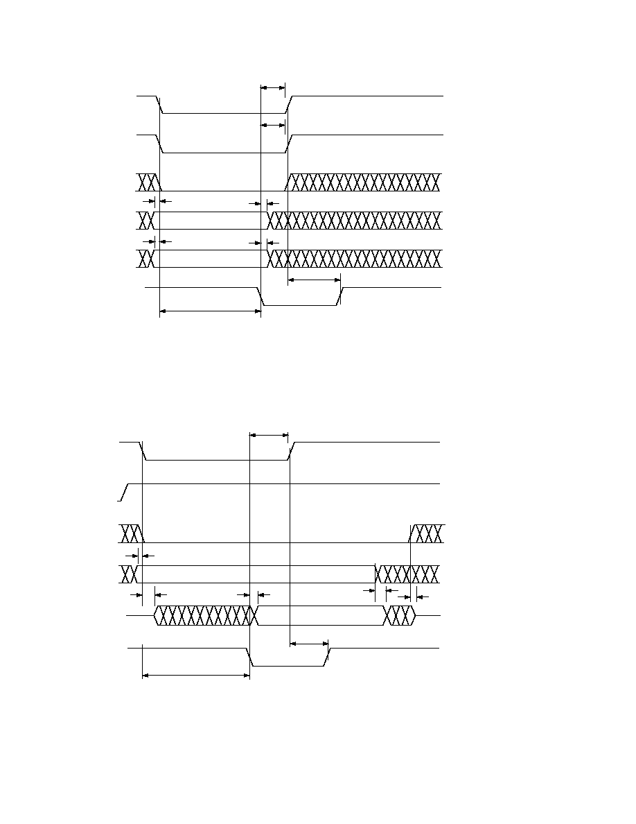
1. t
ACC
ACCESS TIME DEPENDS ON THE ADDRESS ACCESSED. ACCESS TIME IS MEASURED FROM THE FE OF
DS TO THE FE OF DTACK.
2. t
ACC
FAST REQUIRES A MAXIMUM OF FOUR CLK PERIODS AND APPLIES TO A[2:0] = 7, 6, 3, 2, 1
3. t
ACC
MEDIUM REQUIRES A MAXIMUM OF FIVE CLK PERIODS AND APPLIES TO A[2:0] = 4, 5, AND 0 IF THE ACCESS IS TO A CONTROL REGISTER
VERSUS A RAM REGISTER.
4. t
ACC
SLOW REQUIRES A MAXIMUM OF SIX CLK PERIODS AND APPLIES TO A[2:0] = 0 WHEN ACCESSING RAM REGISTERS.
R/
W (WR)
DS (RD)
CS
A[2:0]
D[7:0]
DTACK
(RDY)
t
HRW
t
SAM
t
HAM
t
SAM
t
HAM
t
ACC
VALID ADDRESS
VALID DATA
t
DDTACK
t
HDS
Figure 7. MNM Microport Write Timing Requirements
1. t
ACC
ACCESS TIME DEPENDS ON THE ADDRESS ACCESSED. ACCESS TIME IS MEASURED FROM THE FE OF
DS TO THE FE OF DTACK.
2. t
ACC
FAST REQUIRES A MAXIMUM OF FOUR CLK PERIODS AND APPLIES TO A[2:0] = 7, 6, 3, 2, 1
3. t
ACC
MEDIUM REQUIRES A MAXIMUM OF FIVE CLK PERIODS AND APPLIES TO A[2:0] = 4, 5, AND 0 IF THE ACCESS IS TO A CONTROL REGISTER
VERSUS A RAM REGISTER.
4. t
ACC
SLOW REQUIRES A MAXIMUM OF SIX CLK PERIODS AND APPLIES TO A[2:0] = 0 WHEN ACCESSING RAM REGISTERS.
R/
W (WR)
DS (RD)
CS
A[2:0]
D[7:0]
DTACK
(RDY)
t
SAM
t
ACC
VALID ADDRESS
t
ZD
VALID DATA
t
DD
t
HA
t
ZD
t
HDS
t
DDTACK
Figure 8. MNM Microport Read Timing Requirements

AD6622
7
REV. 0
ABSOLUTE MAXIMUM RATINGS
*
Supply Voltage . . . . . . . . . . . . . . . . . . . . . . . . 0.3 V to +3.6 V
Input Voltage . . . . 0.3 V to VDD +0.3 V (Not 5 V Tolerant)
IN[17:0], QIN, OEN
Input Voltage . . . . . . . . . . . . . 0.3 V to +3.6 V (5 V Tolerant)
CLK,
RESET, DS, R/W, MODE, A[2:0], D[7:0], SYNC, TRST,
TCK, TMS, TDI, SDINA, SDINB, SDINC, SDIND
Output Voltage Swing . . . . . . . . . . . . 0.3 V to VDD + 0.3 V
Load Capacitance . . . . . . . . . . . . . . . . . . . . . . . . . . . . 200 pF
Junction Temperature Under Bias . . . . . . . . . . . . . . . . . 125
°C
Storage Temperature Range . . . . . . . . . . . . 65
°C to +150°C
Lead Temperature (5 sec) . . . . . . . . . . . . . . . . . . . . . . . 280
°C
*Stresses greater than those listed above may cause permanent damage to the
device. These are stress ratings only; functional operation of the devices at these
or any other conditions greater than those indicated in the operational sections of
this specification is not implied. Exposure to absolute maximum rating conditions
for extended periods may affect device reliability.
THERMAL CHARACTERISTICS
128-Lead MQFP:
JA
= 33
°C/W, No Airflow
JA
= 27
°C/W, 200 LFPM Airflow
JA
= 24
°C/W, 400 LFPM Airflow
JC
= 5.5
°C/W
Thermal measurements made in the horizontal position on a
2-layer board.
EXPLANATION OF TEST LEVELS
I.
100% Production Tested.
II.
100% Production Tested at 25
°C, and Sample Tested at
Specified Temperatures.
III. Sample Tested Only.
IV. Parameter Guaranteed by Design and Analysis.
V.
Parameter is Typical Value Only.
VI. 100% Production Tested at 25
°C, and Sample Tested at
Temperature Extremes.
ORDERING GUIDE
Model
Temperature Range
Package Description
Package Option
AD6622AS
40
°C to +70°C (Ambient)
128-Lead MQFP (Metric Quad Flatpack)
S-128A
AD6622S/PCB
Evaluation Board with AD6622 and Software
CAUTION
ESD (electrostatic discharge) sensitive device. Electrostatic charges as high as 4000 V readily
accumulate on the human body and test equipment and can discharge without detection. Although
the AD6622 features proprietary ESD protection circuitry, permanent damage may occur on
devices subjected to high-energy electrostatic discharges. Therefore, proper ESD precautions are
recommended to avoid performance degradation or loss of functionality.
WARNING!
ESD SENSITIVE DEVICE
AD6622
8
REV. 0
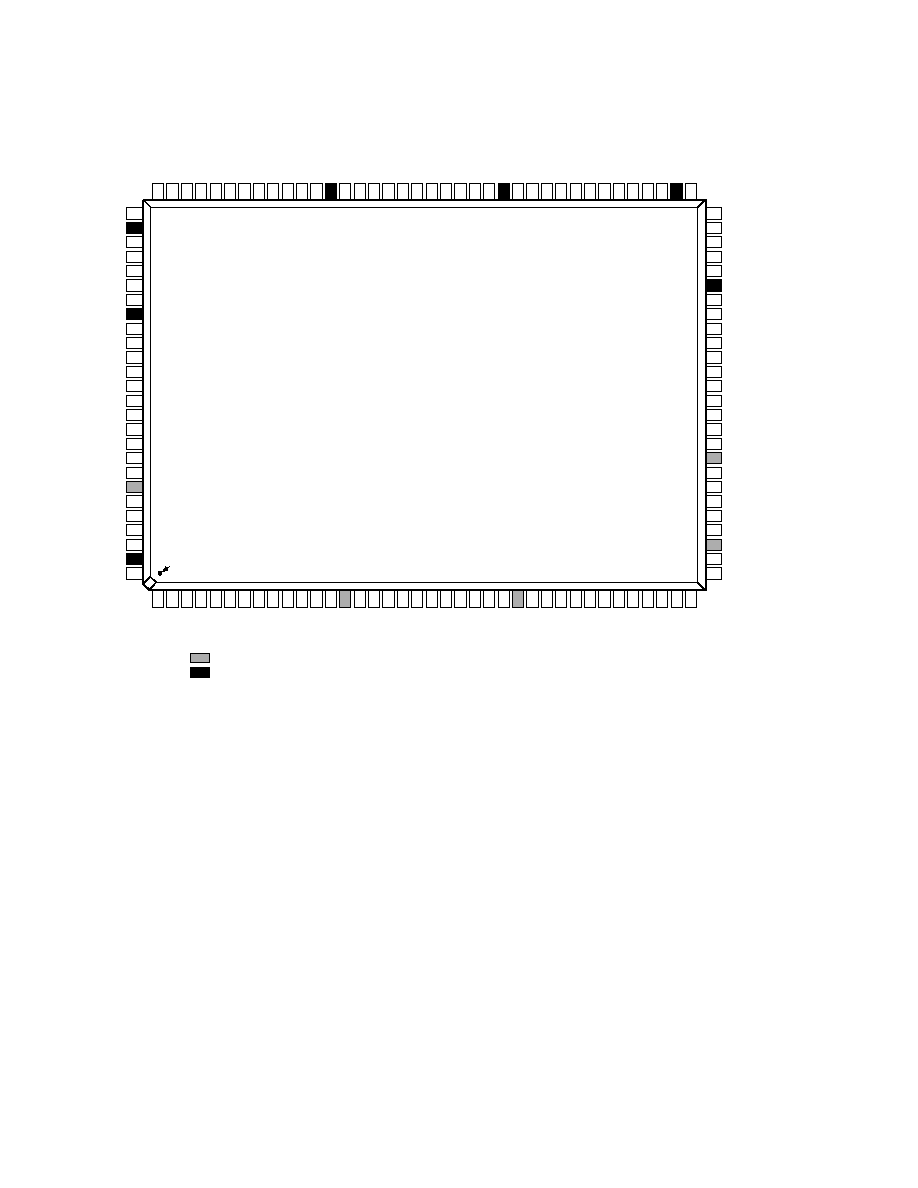
PIN CONFIGURATION
GND
TMS
TDO
TDI
SCLKA
SDFSA
SDINA
SCLKB
SDFSB
GND
GND
GND
SDINB
SCLKC
SDFSC
SDINC
VDD
GND
VDD
VDD
SCLKD
SDFSD
SDIND
GND
VDD
GND
GND
TCK
TRST
GND
GND
IN0
GND
GND
IN1
IN2
IN3
IN4
VDD
IN5
IN6
IN7
IN8
GND
GND
IN16
GND
GND
IN17
QIN
GND
GND
CLK
VDD
GND
GND
IN9
IN10
IN11
IN12
VDD
IN13
IN14
IN15
D7
GND
GND
GND
D6
GND
GND
SYNC
RESET
CS
VDD
A0
A1
A2
MODE
GND
GND
VDD
GND
R/
W(WR)
DTACK(RDY)
DS(RD)
D0
D1
D2
D3
D4
GND
VDD
D5
GND
GND
GND
OEN
GND
GND
GND
OUT0
OUT1
OUT2
GND
OUT3
OUT4
OUT5
OUT6
VDD
OUT7
OUT8
OUT9
OUT10
GND
GND
GND
OUT11
OUT12
OUT13
OUT14
VDD
OUT15
OUT16
OUT17
QOUT
GND
GND
92
93
95
90
91
88
89
87
96
86
94
81
82
83
84
79
80
78
76
77
85
75
73
74
71
72
69
70
67
68
65
98
99
101
97
102
100
11
10
16
15
14
13
18
17
20
19
22
21
12
24
23
26
25
28
27
30
29
32
31
5
4
3
2
7
6
9
8
1
34
33
36
35
38
37
PIN 1
IDENTIFIER
TOP VIEW
(Not to Scale)
AD6622
120
121
122
123
124
125
126
127
128
119
111
118
117
116
115
114
113
112
110
109
108
107
106
105
104
103
41
42
43
44
46
47
48
49
39
45
40
62
61
60
64
63
59
55
50
51
52
53
54
56
57
58
66
DENOTES I/O POWER PIN
DENOTES CORE POWER PIN

AD6622
9
REV. 0
PIN FUNCTION DESCRIPTIONS
Pin Number
Name
Type
Description
1, 35, 9, 1921, 31, 32,
GND
P
Ground Connection
3436, 38, 39, 42, 5254,
6365, 68, 69, 72, 73, 8385,
95, 96, 98, 99, 102, 103,
105, 115117, 126, 128
2
OEN
I
Active High Output Enable Pin (Actively Pulled Down If Not Connected)
(Not 5 V Tolerant)
2729, 2225, 1518, 1013, OUT[17:0]
O/T
Wideband Output Data
68
14, 26, 41, 47, 122
VDD
P
+3.0 V Supply (I/O Supply)
59, 66, 78, 90, 104, 110, 127 VDD
P
+3.0 V Supply (Core Supply)
30
QOUT
O/T
Indicates Q Output Data (Complex Output Mode)
33, 37, 40, 4346, 48
D[7:0]
I/O/T
Microprocessor Interface Data
49
DS (RD)
I
INM Mode: Read Signal, MNM Mode: Data Strobe Signal
50
DTACK (RDY)
O
Acknowledgment of a Completed Transaction (Signals when
µP Port
Is Ready for an Access) Open Drain, Must Be Pulled Up Externally
51
R/
W (WR)
I
Read/Write Line (Write Signal)
55
MODE
I
Sets Microport Mode: MODE = 1, MNM Mode; MODE = 0, INM Mode
5658
A[2:0]
I
Microprocessor Interface Address
60
CS
I
Chip Select, Enable the Chip for
µP Access
61
RESET
I
Active Low Reset Pin (Actively Pulled Up If Not Connected)
62
SYNC
I
SYNC Signal for Synchronizing Multiple AD6622s (Actively Pulled
Down If Not Connected)
67
CLK
I
Input Clock (Actively Pulled Down If Not Connected)
70
QIN
I
Indicates Q Input Data (Complex Input Mode) (Actively Pulled Down
If Not Connected) (Not 5 V Tolerant)
71, 7477, 7982, 8689,
IN[17:0]
I
Wideband Input Data (Allows Cascade of Multiple AD6622 Chips In
9194, 97
a System) (Actively Pulled Down If Not Connected) (Not 5 V Tolerant)
100
TRST
I
Test Reset Pin (Actively Pulled Up If Not Connected)
101
TCK
I
Test Clock Input (Actively Pulled Down If Not Connected)
106
TMS
I
Test Mode Select (Actively Pulled Up If Not Connected)
107
TDO
O
Test Data Output
108
TDI
I
Test Data Input (Actively Pulled Down If Not Connected)
109
SCLKA
O
Serial Clock Output Channel A
111
SDFSA
O
Serial Data Frame Sync Output Channel A
112
SDINA
I
Serial Data Input Channel A (Actively Pulled Down If Not Connected)
113
SCLKB
O
Serial Clock Output Channel B
114
SDFSB
O
Serial Data Frame Sync Output Channel B
118
SDINB
I
Serial Data Input Channel B (Actively Pulled Down If Not Connected)
119
SCLKC
O
Serial Clock Output Channel C
120
SDFSC
O
Serial Data Frame Sync Output Channel C
121
SDINC
I
Serial Data Input Channel C (Actively Pulled Down If Not Connected)
123
SCLKD
O
Serial Clock Output Channel D
124
SDFSD
O
Serial Data Frame Sync Output Channel D
125
SDIND
I
Serial Data Input Channel D (Actively Pulled Down If Not Connected)
AD6622
10
REV. 0
THEORY OF OPERATION
As digital-to-analog converters (DACs) achieve higher sampling
rates, analog bandwidth, and dynamic range, it becomes increas-
ingly attractive to accomplish the first IF stage of a transmitter
in the digital domain. Digital IF signal processing provides
repeatable manufacturing, higher accuracy, and more flexibility
than comparable high-dynamic-range analog designs.
The AD6622 Four-Channel Transmit Signal Processor (TSP) is
designed to bridge the gap between DSPs and high-speed DACs.
The wide range of interpolation factors in each filter stage makes
the AD6622 useful for creating both narrowband and wideband
carriers in a high-speed sample stream. The high-resolution NCO
allows flexibility in frequency planning and supports both digital
and analog air interface standards. The RAM-based architec-
ture allows easy reconfiguration for multimode applications.
The interpolating filters remove unwanted images of signals
sampled at a fraction of the wideband rate. When the channel of
interest occupies far less bandwidth than the wideband output
signal, rejecting out-of-band noise is called "processing gain."
For large interpolation factors, this processing gain allows a
14-bit DAC to express the sum of multiple 16-bit signals sampled
at a lower rate without significantly increasing the noise floor
about each carrier. In addition, the programmable RAM coeffi-
cient stage allows anti-imaging, and static equalization functions
to be combined in a single, cost-effective filter.
The high-speed NCO can be used to tune a quadrature sampled
signal to an IF channel, or the NCO can be directly frequency-
modulated at an IF channel. Multicarrier phase synchronization
pins and phase offset registers allow intelligent management of
the relative phase of the independent RF channels. This capability
supports the requirements for phased array antenna architec-
tures and management of the wideband peak/power ratio to
minimize clipping at the DAC.
The wideband input and output ports allow multiple AD6622s
to be cascaded into a single DAC. The master clock for the
entire system is based on the DAC clock rate (up to 75 MSPS).
The external 18-bit resolution reduces summation of truncation
noise. The wideband ports can be configured for real or quadra-
ture outputs. Quadrature sampled outputs (I and Q) are limited
to half the master clock rate on the shared output bus.
FUNCTIONAL OVERVIEW
The following descriptions explain the functionality of each of
the core sections of the AD6622. Detailed timing, application,
and specifications are described in detail in their respective por-
tions of the data sheet.
SERIAL DATA PORT
The AD6622 has four independent Serial Ports (A, B, C, and
D) of which accepts data to its own channel (1, 2, 3, or 4) of
the device. Each serial port has three pins: SCLK, SDFS, and
SDIN. The SCLK and SDFS pins are outputs that provide
serial clock and framing. The SDIN pins are inputs that accept
channel data. The serial ports do not accept configuration or
control inputs. The serial ports do not accept external clock
or framing signals, although it is possible to synchronize the
AD6622 serial ports to meet an external timing requirement.
The serial clock output, SCLK, is created by a programmable
internal counter that divides down the master clock. When the
channel is reset, SCLK is held low. SCLK starts on the first
rising edge of CLK after Channel Reset is removed (D0 through
D3 of External Address 4). Once active, the SCLK frequency is
determined by the master CLK frequency and the SCLK divider,
according to the equation below. The SCLK divider is a 5-bit
unsigned value located in Channel Register 0x0D. The user must
select the SCLK divider to ensure that SCLK is fast enough to
accept full input sample words at the input sample rate. See the
design example at the end of this section. The maximum SCLK
frequency is 1/2 of the master clock frequency. The minimum
SCLK frequency is 1/64 of the master clock frequency.
f
f
SCLK
SCLK
CLK
DIVIDER
=
×
+
2
1
(
)
(1)
SPORT
SDINA
SDFSA
SCLKA
DATA
RCF
I
Q
CIC
FILTER
I
Q
NCO
DATa
JTAG
TDO
TMS
TRST
TDI
MICROPORT
DS
DTACK
R/
W
D[7:0]
MODE
A[2:0]
CS
SPORT
SDINB
SDFSB
SCLKB
DATA
RCF
I
Q
CIC
FILTER
I
Q
NCO
DATb
SPORT
SDINC
SDFSC
SCLKC
DATA
RCF
I
Q
CIC
FILTER
I
Q
NCO
DATc
SPORT
SDIND
SDFSD
SCLKD
DATA
RCF
I
Q
CIC
FILTER
I
Q
NCO
DATd
SUMMATION
CLK
RESET
QIN
IN
[17:0]
SYNC
OEN
QOUT
OUT
[17:0]
TCK
AD6622
Figure 9. Functional Block Diagram
AD6622
11
REV. 0
The serial data frame sync output, SDFS, is pulsed high for one
SCLK cycle at the input sample rate. The input sample rate is
determined by the master clock divided by channel interpolation
factor. If the SCLK rate is not an integer multiple of the input
sample rate, the SDFS will continually adjust the period by one
SCLK cycle in order to keep the average SDFS rate equal to the
input sample rate. When the channel is in sleep mode, SDFS is
held low. The first SDFS is delayed by the channel reset latency
after the Channel Reset is removed. The channel reset latency
varies dependent on channel configuration.
The serial data input, SDIN, accepts 32-bit words as channel
input data. The 32-bit word is interpreted as two 16 bit two's
complement quadrature words, I followed by Q, MSB first.
The first bit is shifted into the serial port starting on the second
rising edge of SCLK after SDFS goes high, as shown by the
timing diagram below.
CLK
SCLK
SDFS
SDI
CLKn
DATAn
t
DSCLK
t
DSDFS
t
DSDFS
t
SSI
t
HSI
Figure 10. Serial Port Switching Characteristics
As an example of the serial port operation, consider a CLK fre-
quency of 62.208 MSPS and a channel interpolation of 2560.
In that case, the input sample rate is 24.3 kSPS (62.208 MSPS/
2560), which is also the SDFS rate. Substituting, f
SCLK
32 ×
f
SDFS
into the equation below and solving for SCLK
DIVIDER
,
we find the maximum value for SCLK
DIVIDER
according to
Equation 2.
SCLK
f
DIVIDER
SDFS
×
f
CLK
64
1
(2)
Evaluating this equation for our example, SCLK
DIVIDER
must be
less than or equal to 39. Since the SCLK
DIVIDER
channel regis-
ter is a 5-bit unsigned number it can only range from 0 to 31.
Any value in that range will be valid for this example, but if it is
important that the SDFS period is constant, then there is another
restriction. For regular frames, the ratio f
SCLK
/f
SDFS
must be equal
to an integer of 32 or larger. For this example, constant SDFS
periods can only be achieved with an SCLK divider of 19.
In conclusion, the SDFS rate is determined by the AD6622 master
clock rate and the interpolation rate of the channel. The SDFS
rate is equal to the channel input rate. The channel interpola-
tion is equal to RCF interpolation times CIC5 interpolation,
times CIC2 interpolation
L
L
L
L
RCF
CIC
CIC
=
×
×
5
2
(3)
The SCLK rate is determined by the AD6622 master clock
rate and SCLK
DIVIDER
. The SCLK is a divided version of the
AD6622 master CLK. The SCLK divide ratio is determined by
SCLK
DIVIDER
as shown in Equation 2. The SCLK must be fast
enough to input 32 bits of data prior to the next SDFS. Extra
SCLKs are ignored by the serial port.
PROGRAMMABLE INTERPOLATING RAM
COEFFICIENT FILTER (RCF)
Each channel has a fully independent RAM Coefficient Filter
(RCF). The RCF accepts data from the serial port, filters it, and
passes the result to the CIC filter. The RCF implements a FIR
filter with optional interpolation. The FIR filter can produce
impulse responses up to 128 output samples long. The FIR
response may be interpolated up to a factor of 128, although
the best filter performance is usually achieved if the RCF inter-
polation factor is confined to 8 or below.
FIR Filter Implementation
The RCF accepts quadrature samples from the serial port with a
fixed point resolution of 16 bits each, for I and Q.
SERIAL
PORT
DATA
MEM
RCF
RCF COARSE
SCALE
COEFFICIENT
MEM
IQ TO
CIC
FILTER
SDFS
SCLK
SDIN
16,16
ACCUMULATOR
16,16
16,16
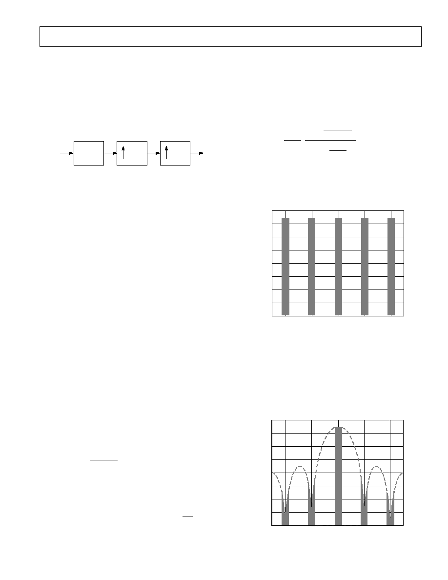
Figure 11. RCF Block Diagram
The AD6622 RCF realizes a sum-of-products filter using a poly-
phase implementation. This mode is equivalent to an interpola-
tor followed by a FIR filter running at the interpolated rate. In
Figure 12, the interpolating block increases the rate by the RCF
interpolation factor (L
RCF
) by inserting L
RCF
-1 zero valued samples
between every input sample. The next block is a filter with a finite
impulse response length (N
RCF
) and an impulse response of h[n],
where n is an integer from 0 to N
RCF
-1.
L
RCF
f
IN
a
b
c
f
IN
L
RCF
N
RCF
TAP
FIR FILTER
h[n]
f
IN
L
RCF
Figure 12. RCF Interpolation
The difference equation for Figure 12 is written below, where
h[n] is the RCF impulse response, b[n] is the interpolated input
sample sequence at point "b" in Figure 12, and c[n] is the out-
put sample sequence at point "c" in the Figure 12.
c n
h k
n
b n
k
N
RCF
[ ]
[
]
[ ]
=
-
×
=
-
0
1
(4)
This difference equation can be described by the transfer func-
tion from point "b" to "c" as shown Equation 5.
H
z
h n
z
bc
n
N
n
RCF
( )
[ ]
=
×
=
-
-
0
1
(5)
The actual implementation of this filter uses a polyphase
decomposition to skip the multiply-accumulates when b[n] is
zero. Compared to the diagram above, this implementation has
the benefits of reducing by a factor of L
RCF
both the time needed to
calculate an output and the required data memory (DMEM). The
price of these benefits is that the user must place the coefficients
into the coefficient memory (CMEM) indexed by the interpo-
lation phase. The process of selecting the coefficients and placing
them into the CMEM is broken into three steps shown below.

AD6622
12
REV. 0
1. Select the Impulse Response Length (N
RCF
) and the Inter-
polation Factor (L
RCF
). The Impulse Response Length
(N
RCF
) is limited in three ways: by the available calculation
time, by the data memory size (DMEM), and by the coeffi-
cient memory size (CMEM). The equation below shows
that N
RCF
is limited to the minimum of these three conditions.
Time
CMEM
Restriction
Restriction
N
L
L
RCF
RCF
×
min
,
,
2
16
128
(6)
DMEM
Restriction
where:
L = L
RCF
× L
CIC5
× L
CIC2
2. The interpolation rate (L
RCF
) may be any integer of N
RCF
ranging from 1 to 128, while meeting the above equation.
Most filter designs can be optimized by choosing the small-
est L
RCF
that does not compromise the image rejection of
the subsequent CIC filter. The quality of an interpolating
filter is a strong function of the N
RCF
/L
RCF
ratio and a weaker
function of N
RCF
. The best filters are usually achieved by
maximizing N
RCF
/L
RCF
(no larger than 16) and then increasing
both N
RCF
and L
RCF
by the same ratio until the filter becomes
time or CMEM limited.
3. Once N
RCF
and L
RCF
are selected, Channel Register 0x0A
is programmed to N
RCF
1, and Channel Register 0x0C is
programmed to N
RCF
/L
RCF
1.
4. Determine the Impulse Response. The impulse response
relative to the RCF output rate can be calculated using ordi-
nary FIR design techniques. In most cases, it is desirable to
precompensate the inband frequency roll-off of the CIC fil-
ter that follows. There are no symmetry requirements, so the
RCF can also be used for static phase equalization. The
impulse response must be quantized to 16-bit two's comple-
ment numbers for the CMEM. The channel center gain and
worst-case peak can be calculated for each of the L
RCF
phases
(p) according to the equations below. A RCF coarse scale
factor (g) that ranges between 0 and 3 is provided to limit
the gain without excessive loss of resolution in the CMEM.
The coarse scale factor is located in Channel Register 0x0D.
ChannelCenterGain
h k
L
p
p
g
RCF
k
N
L
RCF
RCF
=
×
×
+
-
=
2
0
1
[
]
(7)
5. The channel center gain is the response to a constant full-
scale input at every output phase. The summation is split
into phases because the interpolation of the data insures that
only N
RCF
/L
RCF
coefficients can be active for any single output.
For L
RCF
= 1, there is only one phase and the channel center
gain is the simple sum of all the coefficients, scaled by 2
g
. If
the channel center gain is not the same for every value of p,
some or all of the images of the channel center will be
imperfectly rejected by the RCF.
WorstCasePeak
h k
L
p
p
g
RCF
k
N
L
RCF
RCF
=
×
×
+
-
=
2
0
1
| [
]|
(8)
6. The worst-case peak is calculated similarly to the channel
center gain, except that the input sequence swings from full-
scale positive to full-scale negative to match the polarity of the
coefficient by which it will be multiplied, so that each prod-
uct is positive. This results in a maximal that must be less
than one to guarantee no possibility of wrapping. Note that
when L
RCF
is greater than one, each phase may produce its
worst-case peak in response to a different input sequence.
7. Programming DMEM and CMEM. The DMEM must be
initialized to all zeros to avoid any unpredictable start-up
transients since a reset does not clear the memory. The
impulse response h[n] must be reordered by phase for the
CMEM as shown in the code below. Several filters with
impulse lengths that total less than 128 can be programmed
into the CMEM simultaneously and selected later using the
RCF offset pointer (O
RCF
) which is set by Channel Register
0x0B.
/
* Reorder Fir Coefficients for AD6622 CMEM */
for (p=0; p<L_RCF; p++)
for (k=0; k<N_RCF/L_RCF; k++)
CMEM[O_RCF + p*N_RCF/L_RCF + k] = C[k*L_RCF +p];
/
* End of routine */
Table I. RCF Control Registers
Channel
Bit
Address
Width
Description
0x0A
8
7: Reserved (Must Be Written to 0)
60: N
RCF
1
0x0B
8
7: Reserved (Must Be Written to 0)
60: O
RCF
0x0C
8
76: Reserved
54: Reserved (Must Be Written to 0)
30: N
RCF
/L
RCF
1
0x0D
8
76: RCF Coarse Scale:
00 = 0 dB
01 = 6 dB
10 = 12 dB
11 = 18 dB
5: Reserved (Must Be Written to 0)
40: Serial Clock Divider
0x0E
16
150: Reserved
0x0F
16
150: Reserved
0x10
16
150: Reserved (Must Be Written to 0)
0x11
16
150: Reserved (Must Be Written to 0)
0x200x3F
16
150: Data Memory (DMEM)
0x800xFF
16
150: Coefficient Memory (CMEM)
AD6622
13
REV. 0
CASCASDED INTEGRATOR COMB (CIC)
INTERPOLATING FILTER
The I and Q outputs of the RCF stage are interpolated in inte-
ger factors by two cascaded integrator comb (CIC) filters. The
CIC section is separated into three discrete blocks: a fifth order
filter (CIC5), a second order filter (CIC2), and a scaling block
(CIC Scaling). The CIC5 and CIC2 blocks each exhibit a gain
that increases with respect to their interpolation factors, L
CIC5
and L
CIC2
. The product of these gains must be compensated for
in a shared CIC Scaling block.
2
CIC_SCALE
L
CIC5
L
CIC2
CIC_SCALE
CIC5
CIC2
Figure 13. CIC Data Path
CIC Scaling
The CIC5 and CIC2 stages have a baseband gain of L
CIC5
4
×
L
CIC2
. The CIC scaling block is used to avoid numeric overflow
in the CIC stages. The CIC scale block reduces the signal level
without truncation or loss of resolution. The overall gain of the
CIC section is given by Equation 9.
CIC Gain
L
L
CIC
CIC
CIC
Scale
_
_
=
×
×
5
4
2
2
(9)
The value CIC_Scale may range from 0 to 25, and can be inde-
pendently programmed for each channel at Control Register
0x06. CIC_Scale may be safely calculated according Equation 10
to ensure the net gain through the CIC stages.
CIC Scale
ceil
L
L
CIC
CIC
_
(log (
))
=
×
2
5
4
2
(10)
The ceil function is the next highest integer. While this normally
constitutes a small loss, it can be recovered in the RCF scaling.
Likewise, if the RCF output level is known to be less than full
scale, the CIC gain can be increased by reducing CIC_Scale.
CIC5
The CIC5 is a fifth order interpolating cascaded integrator comb
whose impulse response is completely defined by its interpola-
tion factor, L
CIC5
. The value L
CIC5
1 can be independently
programmed for each channel at location 0x09. While this con-
trol register is 8-bits wide, L
CIC5
should be confined to the range
from 1 to 32 to avoid the possibility of internal overflow for
full-scale inputs. The transfer function of the CIC5 is given
by the following equations with respect to the CIC5 output
sample rate, f
SAMP5
.
CIC z
z
z
L
CIC
5
1
1
5
1
5
( )
=
(11)
This polynomial fraction can be completely reduced as follows,
demonstrating a finite impulse response with perfect phase lin-
earity for all values of L
CIC5
.
CIC
z
z
z
e
k
k
L
k
L
j
k
L
CIC
CIC
CIC
5
0
5
1
1
2
5
5 1
5 1
5
( )
=
=
-
-
=
=
-
(12)
The frequency response of the CIC5 can be expressed as follows.
The initial 1/L
CIC5
factor normalizes for the increased rate, which is
appropriate when the samples are destined for a DAC with a
zero order hold output. The maximum gain is (L
CIC5
)
4
at base-
band, but internal registers peak in response to various dynamic
inputs. As long as L
CIC5
is confined to 32 or less, there is no
possibility of overflow at any register.
CIC
f
L
L
f
f
f
L
CIC
CIC
CIC
CIC
5
1
5
5
5
5
5
( )
sin
sin
=
×
(13)
As an example, we will consider an input from the RCF whose
bandwidth is 0.141 of the RCF output rate, centered at base-
band. Interpolation by a factor of five reveals five images, as
shown in Figure 14.
150
2
1
dB
0
1
2
130
110
90
70
50
30
10
10
Figure 14. Unfiltered CIC Interpolation Image
The CIC5 rejects each of the undesired images while passing
the image at baseband. The images of a pure tone at channel
center (dc) are nulled perfectly, but as the bandwidth increases
the rejection is diminished. The lower band edge of the first
image always has the least rejection. In this example, the CIC5
is interpolating by a factor of five and the input signal has a band-
width of 0.141 of the RCF output sample rate. The plot below
shows 110 dBc rejection of the lower band edge of the first
image. All other image frequencies have better rejection.
150
2
1
dB
0
1
2
130
110
90
70
50
30
10
10
Figure 15. Filtered CIC5 Interpolation Images
AD6622
14
REV. 0
Table II lists maximum bandwidth that will be rejected to various
levels for CIC5
interpolation factors from 1 to 32. Figure 15
corresponds to the listing in the 110 dB column and the L
CIC5
= 5 row. It is worth noting that the rejection of the CIC5 improves
as the interpolation factor increases.
Table II. CIC5 Alias Protection
110 dB
100 dB
90 dB
80 dB
70 dB
1
Full
Full
Full
Full
Full
2
0.101
0.127
0.160
0.203
0.256
3
0.126
0.159
0.198
0.246
0.307
4
0.136
0.170
0.211
0.262
0.325
5
0.141
0.175
0.217
0.269
0.333
6
0.143
0.178
0.220
0.272
0.337
7
0.144
0.179
0.222
0.275
0.340
8
0.145
0.180
0.224
0.276
0.341
9
0.146
0.181
0.224
0.277
0.342
10
0.146
0.182
0.225
0.278
0.343
11
0.147
0.182
0.226
0.278
0.344
12
0.147
0.182
0.226
0.279
0.344
13
0.147
0.183
0.226
0.279
0.345
14
0.147
0.183
0.226
0.279
0.345
15
0.148
0.183
0.227
0.280
0.345
16
0.148
0.183
0.227
0.280
0.345
17
0.148
0.183
0.227
0.280
0.346
18
0.148
0.183
0.227
0.280
0.346
19
0.148
0.183
0.227
0.280
0.346
20
0.148
0.184
0.227
0.280
0.346
21
0.148
0.184
0.227
0.280
0.346
22
0.148
0.184
0.227
0.280
0.346
23
0.148
0.184
0.227
0.280
0.346
24
0.148
0.184
0.227
0.280
0.346
25
0.148
0.184
0.227
0.281
0.346
26
0.148
0.184
0.227
0.281
0.346
27
0.148
0.184
0.227
0.281
0.346
28
0.148
0.184
0.227
0.281
0.346
29
0.148
0.184
0.227
0.281
0.346
30
0.148
0.184
0.227
0.281
0.346
31
0.148
0.184
0.227
0.281
0.346
32
0.148
0.184
0.228
0.281
0.346
CIC2
The CIC2 is a second-order interpolating cascaded integrator
comb whose impulse response is completely defined by its inter-
polation factor, L
CIC2
. The value L
CIC2
1 can be independently
programmed for each channel at location 0x08. While this con-
trol register is 8 bits wide, L
CIC2
should be confined to the ranges
shown by the table below according to the interpolation factor
of the CIC5. Exceeding the recommended guidelines may result in
overflow for input sequences at or near full scale. While relatively
small values of L
CIC5
allow for the larger overall interpolation
factors with minimal power consumption, L
CIC5
should be maxi-
mized to achieve the best overall image rejection.
Table III. Maximum L
CIC2
Limits
L
CIC5
Max L
CIC2
119
256
20
209
21
172
22
143
23
119
24
101
25
85
26
73
27
63
28
54
29
47
30
41
31
36
32
32
The transfer function of the CIC2 is given by the following
equations with respect to the CIC2 output sample rate, f
OUT
.
CIC
z
z
z
L
CIC
2
1
1
2
1
2
( )
=
(14)
This polynomial fraction can be completely reduced as follows,
demonstrating a finite impulse response with perfect phase lin-
earity for all values of L
CIC2
.
CIC
z
z
z
e
k
k
L
j
k
L
k
L
CIC
CIC
CIC
2
0
2
1
2
1
2
2 1
2
2 1
( )
=
=
-
-
=
-
=
(15)
The frequency response of the CIC2 can be expressed as follows.
The maximum gain is L
CIC2
at baseband. The initial 1/L
CIC2
factor normalizes for the increased rate, which is appropriate
when the samples are destined for a DAC with a zero order hold
output.
CIC
f
L
L
f
f
f
f
CIC
CIC
OUT
OUT
2
1
2
2
2
( )
sin
sin
=
×
(16)
As an example, we will consider an input from the CIC5 whose
bandwidth is 0.0033 of the CIC5 rate, centered at baseband.
Interpolation by a factor of five reveals five images, as shown
below.
AD6622
15
REV. 0
150
2
1
dB
0
1
2
130
110
90
70
50
30
10
10
Figure 16. Unfiltered CIC2 Interpolation Images
The CIC2 rejects each of the undesired images while passing
the image at baseband. The images of a pure tone at channel
center (dc) are nulled perfectly, but as the bandwidth increases
the rejection is diminished. The lower band edge of the first
image always has the least rejection. In this example, the CIC2
is interpolating by a factor of five and the input signal has a band-
width of 0.0033 of the CIC5 output sample rate. Figure 17
shows 110 dBc rejection of the lower band edge of the first
image. All other image frequencies have better rejection.
150
2
1
dB
0
1
2
130
110
90
70
50
30
10
10
Figure 17. Filtered CIC2 Interpolation Images
Table IV lists maximum bandwidth that will be rejected to various
levels for CIC2
interpolation factors from 1 to 32. The example
above corresponds to the listing in the 110 dB column and
the L
CIC2
= 5 row. It is worth noting that the rejection of the
CIC2 improves as the interpolation factor increases.
Table IV. CIC2 Alias Protection
110 dB
100 dB
90 dB
80 dB
70 dB
1
Full
Full
Full
Full
Full
2
0.0023
0.0040
0.0072
0.0127
0.0226
3
0.0029
0.0052
0.0093
0.0165
0.0292
4
0.0032
0.0057
0.0101
0.0179
0.0316
5
0.0033
0.0059
0.0105
0.0186
0.0328
6
0.0034
0.0060
0.0107
0.0189
0.0334
7
0.0034
0.0061
0.0108
0.0192
0.0338
8
0.0035
0.0062
0.0109
0.0193
0.0341
9
0.0035
0.0062
0.0110
0.0194
0.0343
10
0.0035
0.0062
0.0110
0.0195
0.0344
11
0.0035
0.0062
0.0110
0.0195
0.0345
12
0.0035
0.0062
0.0111
0.0196
0.0346
13
0.0035
0.0062
0.0111
0.0196
0.0346
14
0.0035
0.0063
0.0111
0.0196
0.0347
15
0.0035
0.0063
0.0111
0.0197
0.0347
16
0.0035
0.0063
0.0111
0.0197
0.0347
17
0.0035
0.0063
0.0111
0.0197
0.0348
18
0.0035
0.0063
0.0111
0.0197
0.0348
19
0.0035
0.0063
0.0111
0.0197
0.0348
20
0.0035
0.0063
0.0111
0.0197
0.0348
21
0.0035
0.0063
0.0111
0.0197
0.0348
22
0.0035
0.0063
0.0111
0.0197
0.0348
23
0.0035
0.0063
0.0111
0.0197
0.0348
24
0.0035
0.0063
0.0112
0.0197
0.0348
25
0.0035
0.0063
0.0112
0.0198
0.0349
26
0.0035
0.0063
0.0112
0.0198
0.0349
27
0.0035
0.0063
0.0112
0.0198
0.0349
28
0.0035
0.0063
0.0112
0.0198
0.0349
29
0.0035
0.0063
0.0112
0.0198
0.0349
30
0.0035
0.0063
0.0112
0.0198
0.0349
31
0.0035
0.0063
0.0112
0.0198
0.0349
32
0.0035
0.0063
0.0112
0.0198
0.0349
AD6622
16
REV. 0
NUMERICALLY CONTROLLED OSCILLATOR (NCO) TUNER
Each channel has a fully independent tuner. The tuner accepts
data from the CIC filter, tunes it to a digital Intermediate Fre-
quency (IF), and passes the result to a shared summation block.
The tuner consists of a 32-bit quadrature NCO and a Quadrature
Amplitude Mixer (QAM). The NCO serves as a local oscillator
and the QAM translates the interpolated channel data from
baseband to the NCO frequency. The worst-case spurious signal
from the NCO is better than 100 dBc for all output frequencies.
The tuner can produce real or complex outputs as requested by
the shared summation block.
In the complex mode, the NCO serves as a quadrature local
oscillator running at f
CLK
/2, capable of producing any frequency
between f
CLK
/4 and +f
CLK
/4 with a resolution of f
CLK
/2
33
(0.0087 Hz for f
CLK
= 75 MHz).
In the real mode, the NCO serves as a quadrature local oscilla-
tor running at f
CLK
, capable of producing any frequency between
f
CLK
/2 and +f
CLK
/2 with a resolution of f
CLK
/2
32
(0.017 Hz for
f
CLK
= 75 MHz). The quadrature portion of the output is dis-
carded. Negative frequencies are distinguished from positive
frequencies solely by spectral inversion.
The digital IF is calculated using Equation 17 below.
f
f
NCO frequency
IF
NCO
=
×
_
2
32
(17)
where:
NCO_frequency is the value written to 0x02, f
IF
is the desired
intermediate frequency, and f
NCO
is f
CLK
/2 for complex outputs
and f
CLK
for real outputs.
Phase Dither
The AD6622 provides a phase dither option for improving the
spurious performance of the NCO. Phase dither is enabled by
writing a one to Bit 3 of Channel Register 0x01. When phase
dither is enabled, spurs due to phase truncation in the NCO are
randomized. The choice of whether phase dither is used in a
system will ultimately be decided by the system goals and the
choice of IF frequency. The 18 most significant bits of the phase
accumulator are used by the angle to Cartesian conversion. If
the NCO frequency has all zeroes below the 18th bit, then phase
dither has no effect. If the fraction below the 18th bit is near a
1/2 or 1/3, etc., of the 18th bit, then spurs will accumulate sepa-
rated from the IF by 1/2 or 1/3, etc., of the CLK frequency. The
smaller the denominator of this residual fraction, the larger the
spurs due to phase truncation will be. If the phase truncation spurs
are unacceptably high for a given frequency, the phase dither can
reduce these at the penalty of a slight elevation in total error
energy. If the phase truncation spurs are small, phase dither
will not be effective in reducing them further, but a slight eleva-
tion in total error energy will occur.
Amplitude Dither
Amplitude dither can also be used to improve spurious perfor-
mance of the NCO. Amplitude dither is enabled by writing a one
to Bit 4 of Channel Register at 0x01. When enabled, amplitude
dither can reduce spurs due to truncation at the input to the QAM.
If the entire frequency word is close to a fraction that has a
small denominator, the spurs due to amplitude truncation will
be large and amplitude dither will spread these spurs effectively.
Amplitude dither also will increase the total error energy by
approximately 3 dB. For this reason amplitude dither should be
used judiciously.
Phase Offset
The phase offset (Channel Register 0x04) adds an offset to the
phase accumulator of the NCO. This is a 16-bit register that is
interpreted as a 16-bit unsigned integer. Phase offset ranges
from 0 to nearly 2
radians with a resolution of /32768 radians.
This register allows multiple NCOs to be synchronized to pro-
duce sine waves with a known phase relationship.
NCO Frequency Update and Phase Offset Update Hold-Off
Counters
The update of both the NCO Frequency and Phase Offset can
be synchronized with internal hold-off counters. Both of these
counters are 16-bit unsigned integers and are clocked at the
master CLK rate. These hold-off counters, used in conjunction
with the frequency or phase offset registers, allow Beam Form-
ing and Frequency Hopping. See the Synchronization section of
this data sheet for additional details. The NCO phase can also
be cleared on Sync (set to 0x0000) by setting Bit 2 of Channel
Register 0x01 high.
NCO Output Scale
The output of the NCO can be scaled in four steps of 6 dB each
via Channel Register 0x01, Bits 10. Table V is a table of the
control scale. The NCO always has loss to accommodate the
possibility that both the I and Q inputs may reach full-scale simul-
taneously, resulting in a 3 dB input magnitude.
Table V. Control Scale
0x01 Bit 1
0x01 Bit 0
NCO Output Level
0
0
6 dB
0
1
12 dB
1
0
18 dB
1
1
24 dB
16
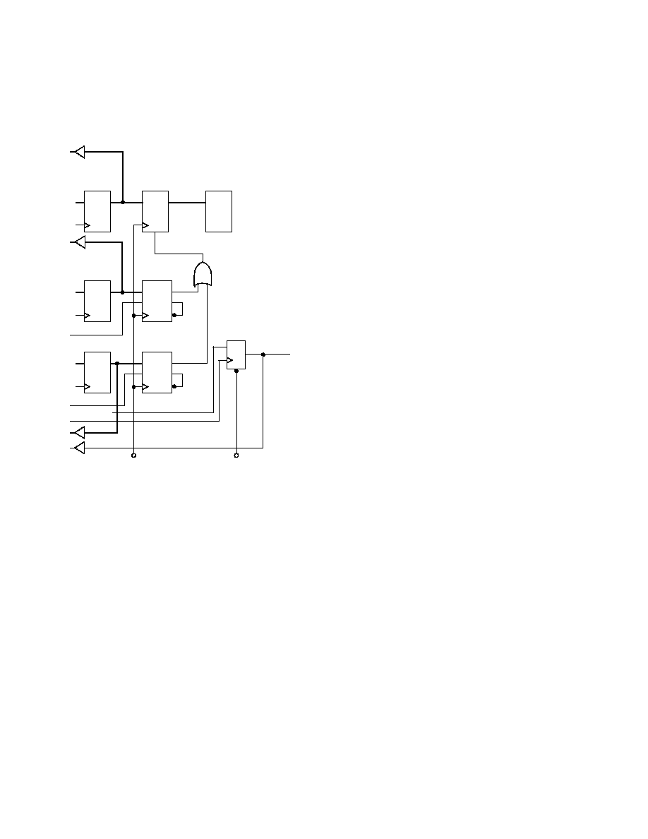
PHASE
OFFSET
NCO
FREQUENCY
WORD
16
32
32
32
32
I
COS
Q
SIN
I DATA
FROM CIC5
Q DATA
FROM CIC5
ON
OFF
ON
OFF
CLK
PHASE
AMPLITUDE
PN
GEN.
PN
GEN.
D
Q
D
Q
ANGLE TO
CARTESIAN
CONVERSION
Figure 18. NCO Block Diagram
AD6622
17
REV. 0
SUMMATION BLOCK
The summation block of the AD6622 serves to combine the out-
puts of each channel to create a composite multicarrier signal.
The four channels are summed together and the result is then
added with the 18-bit wideband input bus (IN[17:0]). The final
summation is then driven on the 18-bit wideband output bus
(OUT[17:0]) on the rising edge of the high speed clock. If the
OEN input is high, this output bus is three-stated. If the OEN
input is low, this bus will be driven by the summed data. The OEN
is active high to allow the wideband output bus to be connected
to other buses without using extra logic. Most other buses (like
374-type registers) require a low output enable, which is opposite
the AD6622 OEN, thus eliminating extra circuitry.
The wideband output bus may be interpreted as a two's comple-
ment number or as an offset binary number as defined by Bit 1
of the Summation Mode Control Register at address 0x000.
When this bit is high, the wideband output is in two's comple-
ment mode and when it is low it is configured for offset binary
output data.
The MSB (Bit 17) of the wideband output bus is typically used as
a guard bit for the purpose of clipping the wideband output
bus when Bit 0 of the Summation Mode Control Register at
address 0x000 is high. If clip detection is enabled, Bit 17 of the
output bus is not used as a data bit. Instead, Bit 16 will become the
MSB and be connected to the MSB of the DAC. Configuring
the DAC in this manner gives the summation block a gain of 0 dB.
When clip detection is not enabled and Bit 17 is used as a data
bit, then the summation block will have a gain of 6.02 dB.
There are two data output modes. The first is offset binary. This
mode is used only when driving offset binary DACs. Two's comple-
ment mode may be used in one of two circumstances. The first is
when driving a DAC that accepts two's complement data. The
second is when driving another AD6622 in cascade mode.
When clipping is enabled, the two's complement mode output
bus will clip to 0x0FFFF for output signals more positive than the
output can express, and it will clip to 0x10000 for signals more
negative than the output can express. In offset binary mode the
output bus will clip to 0x1FFFF for output signals more positive
than the output can express, and it will clip to 0x00000 for signals
more negative than the output can express.
Table VI. Numerical Data Representation
Number Represented
Output Representation
+Full-Scale Two's Complement
0x0FFFF
Full-Scale Two's Complement
0x10000
+Full-Scale Offset Binary
0x1FFFF
Full-Scale Offset Binary
0x00000
The wideband input is always interpreted as an 18-bit two's
complement number and is typically connected to the wideband
output bus of another AD6622 in order to send more than four
carriers to a single DAC. The Output Bus of the proceeding
AD6622 should be configured in two's complement mode and
clip detection disabled. The 18-bit resolution ensures that the
noise and spur performance of the wideband data stream does
not become the limiting factor as large numbers of carriers are
summed.
There is a two-clock cycle latency from the wideband input
bus to the wideband output bus. This latency may be calibrated
out of the system by use of the start hold-off counter. The pre-
ceding AD6622 in a cascaded chain can be started two high-speed
clock cycles before the following AD6622 is started and the data
from each AD6622 will arrive at the DAC on the same clock
cycle. In systems where the individual signals are not corre-
lated, this is usually not necessary.
The AD6622 is capable of outputting both real and complex
data. When in real mode, the QIN input is tied low signaling that
all inputs on the wideband input bus are real and that all outputs
on the wideband output bus are real. The wideband input bus
will be pulled low and no data will be added to the composite
signal if this port is unused (not connected).
If complex data is desired, there are two ways this can be obtained.
The first method is simply to set the QIN input of the AD6622
high and set the wideband input bus low. This allows the AD6622
to output complex data on the wideband output bus. The I
data samples would be identified when QOUT is low and the Q
data samples would be identified when QOUT is high. The
second method of obtaining complex data is to provide a QIN
signal that toggles on every rising edge of the high-speed clock.
This could be obtained by connecting the QOUT of another
AD6622 to QIN. In a cascaded system the QIN of the first AD6622
in the chain would typically be tied high and the QOUT of the first
AD6622 would be connected to the QIN of the following part.
All AD6622s will synchronize themselves to the QIN input so
that the proper samples are always paired and the wideband out-
put bus represents valid complex data samples.
Table VII. QIN, QOUT Functionality
Wideband
Output Data Type
QIN
Input IN[17:0]
OUT[17:0]
QOUT
Low
Real
Real
Low
High
Zero
Complex
Pulse
Pulsed
Complex
Complex
Pulse
TWO'S COMPLEMENT,
CLIPPING DISABLED
AD6622
Q
IN
IN
[17:0]
LOGIC1
LOGIC0
Q
OUT
OUT
[17:0]
AD6622
Q
IN
IN
[17:0]
OUT
[16:3]
14-BIT
DAC
OFFSET BIN,
CLIPPING
ENABLED
Figure 19. Cascade Operation of Two AD6622s
SYNCHRONIZATION
Three types of synchronization can be achieved with the AD6622.
These are Start, Hop, and Beam. Each is described in detail below.
The synchronization is accomplished with the use of a shadow
register and a hold-off counter. See Figure 20 for a simplified
schematic of the NCO Shadow Register and NCO Freq Hold-
Off Counter to understand basic operation. Enabling the clock
(AD6622 CLK) for the Hold-Off Counter can occur with either
a Soft Sync (via the Microport), or a Pin Sync (via the AD6622
sync pin, Pin 62). The functions that include shadow registers
to allow synchronization include:
1. Start
2. Hop (NCO Frequency)
3. Beam (NCO Phase Offset)
AD6622
18
REV. 0
Start refers to the start-up of an individual channel, chip, or
multiple chips. If a channel is not used, it should be put in the
Sleep Mode to reduce power dissipation. Following a hard reset
(low pulse on the AD6622
RESET pin), all channels are placed
in the Sleep Mode.
NCO
FREQUENCY
REGISTER
32
32
D
Q
32
D
Q
NCO
REGISTER
NCO PHASE
ACCUMULATOR
HOP
HOLD-OFF
16
16
D
Q
D
HOLD-OFF
COUNTER
PL
C = 1
C = 0
ENA
START
HOLD-OFF
16
16
D
Q
D
START
COUNTER
PL
C = 1
C = 0
ENA
START SYNC
D
Q
SET
SLEEP
CLK
RESET
PIN
HOP SYNC
EXTERNAL
ADDRESS 4
ENA
MICROPROCESSOR INTERFACE
Figure 20. NCO Shadow Register and Hold-Off Counter
Start with No Sync
If no synchronization is needed to start multiple channels or
multiple AD6622s, the following method can be used to ini-
tialize the device.
1. To program a channel, it must first be set to the Program
Mode (bit high) and Sleep Mode (bit high) (External Address
4). The Program Mode allows programming of data memory
and coefficient memory (all other registers are programmable
whether or not in Program Mode). Since no synchronization
is used all sync bits are set low (External Address 5). All
appropriate control and memory registers (filter) are then
loaded. The Start Update Hold-Off Counter (0x00) should
be set to 0.
2. Set the appropriate program and sleep bits low (External
Address 4). This enables the channel. The channel must have
Program and Sleep Mode low to activate a channel.
Start with Soft Sync
The AD6622 includes the ability to synchronize channels or chips
under microprocessor control. One action to synchronize is the
start of channels or chips. The Start Update Hold-Off Counter
(0x00) in conjunction with the start bit and sync bit (External
Address 5) allow this synchronization. Basically the Start Update
Hold-Off Counter delays the start of a channel(s) by its value
(number of AD6622 CLKs). The following method is used to
synchronize the start of multiple channels via microprocessor
control.
1. Set the appropriate channels to sleep mode (a hard reset
to the AD6622
RESET pin brings all four channels up in
sleep mode).
2. Write the Start Update Hold-Off Counter(s) (0x00) to the
appropriate value (greater than 1 and less than 2
16
1). If the
chip(s) is not initialized, all other registers should be loaded
at this step.
3. Write the Start bit and the SyncX(s) bit high (External
Address 5).
4. This starts the Start Update Hold-Off Counter counting
down. The counter is clocked with the AD6622 CLK signal.
When it reaches a count of one the Sleep bit of the appropri-
ate channel(s) is set low to activate the channel(s).
Start with Pin Sync
A sync pin is provided on the AD6622 to provide the most
accurate synchronization, especially between multiple AD6622s.
Synchronization of start with an external signal is accomplished
with the following method.
1. Set the appropriate channels to sleep mode (a hard reset to
the AD6622
RESET pin brings all four channels up in
sleep mode).
2. Write the Start Update Hold-Off Counter(s) (0x00) to the
appropriate value (greater than 1 and less than 2
16
1). If the
chip(s) is not initialized, all other registers should be loaded
at this step.
3. Set the start on pin sync bit and the appropriate sync pin
enable high (0x001).
4. When the sync pin is sampled high by the AD6622 CLK, it
enables the countdown of the Start Update Hold-Off Counter.
The counter is clocked with the AD6622 CLK signal. When
it reaches a count of one, the sleep bit of the appropriate
channel(s) is set low to activate the channel(s).
Hop is a jump from one NCO frequency to a new NCO frequency.
This change in frequency can be synchronized via microproces-
sor control or an external sync signal as described below.
To set the NCO frequency without synchronization the follow-
ing method should be used.
Set Freq No Hop
1. Set the NCO Freq Hold-Off Counter to 0.
2. Load the appropriate NCO frequency. The new frequency
will immediately be loaded to the NCO.
Hop with Soft Sync
The AD6622 includes the ability to synchronize a change in
NCO frequency of multiple channels or chips under micro-
processor control. The NCO Freq Hold-Off Counter (0x03), in
conjunction with the hop bit and the sync bit (Ext Address 5),
allow this synchronization. Basically the NCO Freq Hold-Off
Counter delays the new frequency from being loaded into the
NCO by its value (number of AD6622 CLKs). The following
method is used to synchronize a hop in frequency of multiple chan-
nels via microprocessor control.
AD6622
19
REV. 0
1. Write the NCO Freq Hold-Off (0x03) Counter to the appro-
priate value (greater than 1 and less then 2
16
1).
2. Write the NCO Frequency Register(s) to the new desired
frequency.
3. Write the hop bit and the sync(s) bit high (Ext Address 5).
4. This starts the NCO Freq Hold-Off Counter counting down.
The counter is clocked with the AD6622 CLK signal. When
it reaches a count of one, the new frequency is loaded into
the NCO.
Hop with Pin Sync
A sync pin is provided on the AD6622 to provide the most
accurate synchronization, especially between multiple AD6622s.
Synchronization of hopping to a new NCO frequency with an
external signal is accomplished with the following method.
1. Write the NCO Freq Hold-Off Counter(s) (0x03) to the
appropriate value (greater than 1 and less than 2
16
1).
2. Write the NCO Frequency register(s) to the new desired
frequency.
3. Set the hop on pin sync bit and the appropriate sync pin
enable high (0x001).
4. When the sync pin is sampled high by the AD6622 CLK this
enables the countdown of the NCO Freq Hold-Off Counter.
The counter is clocked with the AD6622 CLK signal. When
it reaches a count of one the new frequency is loaded into the
NCO.
Beam is a change in phase for a particular channel and can be
synchronized with respect to other channels or AD6622s. This
change in phase can be synchronized via microprocessor control
or an external sync signal as described below.
To set the amplitude without synchronization the following
method should be used.
Set Phase No Beam
1. Set the NCO Phase Offset Update Hold-Off Counter (0x05)
to 0.
2. Load the appropriate NCO Phase Offset (0x04). The NCO
Phase Offset will be immediately loaded.
Beam with Soft Sync
The AD6622 includes the ability to synchronize a change in
NCO phase of multiple channels or chips under microprocessor
control. The NCO Phase Offset Update Hold-Off Counter, in
conjunction with the beam bit and the sync bit (Ext Address 5),
allow this synchronization. Basically the NCO Phase Offset
Update Hold-Off Counter delays the new phase from being
loaded into the NCO/RCF by its value (number of AD6622
CLKs). The following method is used to synchronize a beam-in
phase of multiple channels via microprocessor control.
1. Write the NCO Phase offset Update Hold-Off Counter (0x05)
to the appropriate value (greater than 1 and less then 2
16
1).
2. Write the NCO Phase Offset Register(s) to the new desired
phase and amplitude.
3. Write the beam bit and the sync(s) bit high (External
Address 5).
4. This starts the NCO Phase Offset Update Hold-Off counter
counting down. The counter is clocked with the AD6622
CLK signal. When it reaches a count of one, the new phase
is loaded into the NCO.
Beam with Pin Sync
A sync pin is provided on the AD6622 to provide the most
accurate synchronization, especially between multiple AD6622s.
Synchronization of beaming to a new NCO Phase Offset with an
external signal is accomplished with the following method.
1. Write the NCO Phase Offset Hold-Off (0x05) counter(s) to
the appropriate value (greater than 1 and less than 2
16
1).
2. Write the NCO Phase Offset register(s) to the new desired
phase and amplitude.
3. Set the beam on pin sync bit and the appropriate sync pin
enable high (0x001).
4. When the sync pin is sampled high by the AD6622 CLK, it
enables the countdown of the NCO Phase Offset Hold-Off
Counter. The counter is clocked with the AD6622 CLK sig-
nal. When it reaches a count of one, the new phase is loaded
into the NCO registers.
JTAG INTERFACE
The AD6622 supports a subset of IEEE Standard 1149.1
specifications. For additional details of the standard, please
see "IEEE Standard Test Access Port and Boundary-Scan
Architecture," IEEE-1149 publication from IEEE.
The AD6622 has five pins associated with the JTAG interface.
These pins are used to access the on-chip Test Access Port and
are listed in Table VIII.
Table VIII. JTAG Pin List
Name
Pin Number
Description
TRST
100
Test Access Port Reset
TCK
101
Test Clock
TMS
106
Test Access Port Mode Select
TDI
108
Test Data Input
TDO
107
Test Data Output
The AD6622 supports four op codes as shown in Table IX.
These instructions set the mode of the JTAG interface.
Table IX. JTAG Op Codes
Instruction
Op Code
IDCODE
10
BYPASS
11
SAMPLE/PRELOAD
01
EXTEST
00
The Vendor Identification Code can be accessed through the
IDCODE instruction and has the following format.
Table X. JTAG ID String
MSB
Part
Manufacturing
LSB
Version
Number
ID #
Mandatory
000
0010
000 1110 0101
1
0111
1000
0000
A BSDL file for this device is available from Analog Devices, Inc.
Contact Analog Devices Inc. for more information.

AD6622
20
REV. 0
SCALING
Proper scaling of the wideband output is critical to maximize the
spurious and noise performance of the AD6622. A relatively small
overflow anywhere in the data path can cause the spurious free
dynamic range to drop precipitously. Scaling down the output
levels also reduces dynamic range relative to an approximately
constant noise floor. A well-balanced scaling plan at each point
in the signal path will be rewarded with optimum performance.
The scaling plan can be separated into two parts: multicarrier
scaling and single-carrier scaling.
Multicarrier Scaling
An arbitrary number of AD6622s can be cascaded to create a
composite digital IF with many carriers. As the number of carriers
increases, the peak-to-rms ratio of the composite digital IF will
increase as well. It is possible and beneficial to limit the peak-to-
rms ratio through careful frequency planning and controlled phase
offsets. Nevertheless, in most cases with a large number of carriers,
the worst-case peak is an unlikely event.
The AD6622 immediately preceding the DAC can be programmed
to clip rather than wrap around (see the Summation Block descrip-
tion). For a large number of carriers, a rare but finite chance
of clipping at the AD6622 wideband output will result in superior
dynamic range compared to lowering each carrier level until
clipping is impossible. This will also be the case for most DACs.
Through analysis or experimentation, an optimal output level of
individual carriers can be determined for any particular DAC.
Single-Carrier Scaling
Once the optimal power level is determined for each carrier, one
must determine the best way to achieve that level. The maximum
SNR can be achieved by maximizing the intermediate power
level at each processing stage. This can be done by assuming the
proper level at the output and working backwards along the signal
path: Summation, NCO, CIC, and finally, RCF.
The summation block is intended to combine multiple carriers,
with each carrier at least 6 dB below full scale. For this configu-
ration, the AD6622 driving the DAC should have clip detection
enable. OUT17 becomes a clip indicator that reports clipping in
both polarities. If the DAC requires offset binary outputs, the
internal offset binary conversion should be enabled as well. Any
preceding cascaded AD6622s should disable clip detection and
offset binary conversion. The IN17IN0 of the first AD6622 in the
cascade should be grounded. See the Summation Block section
for details. In this configuration, intermediate OUT17s will
serve as guard bits that allow intermediate sums to exceed full
scale. As long as the final output does not exceed 6 dB over full
scale, the clip detector will perform correctly.
If a single carrier needs to exceed 6 dB full scale, hardwired
scaling can be accomplished according to the table below. This
is most useful when the AD6622 is processing a Single Wide-
band Carrier such as UMTS or CDMA 2000.
Table XI. Output Bit Scaling
M
ax Single-
Connect to
Clip
Offset Binary
Carrier Level
DAC MSB
Detect
Compensation
12.04 dB
OUT17
N/A
Internal
6.02 dB
OUT16
±
Internal
0 dB
OUT15
+Only
0x18000
+6.02 dB
OUT14
+Only
0x1C000
+12.04 dB
OUT13
+Only
0x1E000
+18.06 dB
OUT12
+Only
0x1F000
+24.08 dB
OUT11
+Only
0x1F800
The NCO/Tuner is equipped with an output scalar that ranges
from 6.02 dB to 24.08 dB below full scale, in 6.02 dB steps.
See the NCO/Tuner section for details. The best SNR will be
achieved by maximizing the input level to the NCO and using
the largest possible NCO attenuation. For example, to achieve
an output level 20 dB below full scale, one should set the CIC
output level to 1.94 dB below full scale and attenuate by
18.06 dB in the NCO.
The CIC is equipped with an output scalar that ranges from
0 dB to 150.51 dB below full scale in 6.02 dB steps. This large
attenuation is necessary to compensate for the potentially large
gains associated with CIC interpolation. See the CIC section for
details. For example to achieve an output level of 1.94 dB below
full scale, with a CIC5 interpolation of 27 (114.51 dB gain) and
a CIC2 interpolation of 3 (9.54 dB gain), one should set the
CIC_Scale to 20 and the RCF output level to 5.59 dB below
full scale.
.
.
.
.
.
1 94
9 54
114 51
20
6 02
5 59
+
×
=
(18)
The RCF is equipped with an output scalar that ranges from 0 dB
to 18.06 dB below full scale in 6.02 dB steps. This attenuation
can be used to compensate for filter gain in the RCF. For example,
if the desired RCF output is 5.59 dB and the maxim gain of the
RCF coefficients is 11.04 dB, then the RCF_Coarse_Scale should
be set to two and the coefficients should be scaled so that the
largest coefficient is 4.59 dB below full scale. The largest pos-
sible gain of the RCF coefficients is when the largest coefficient
of the impulse response is normalized to one. This means that
all of the coefficients are as large as possible so the sum of the
coefficients are as large as possible. This maximum gain will
determine the RCF_Coarse_Scale, which should be used to
make the total RCF gain between 0 dB and 6.02 dB. After the
RCF_Coarse_Scale is chosen, the coefficients can be rescaled, as
in the example, to set the total RCF gain to a desired level. See the
RCF section for additional information.
.
.
.
.
5 59
11 04
2
6 02
4 59
+ ×
=
(19)
Finally, as described in the RCF section, there may be a worst-
case peak of a phase that is larger than the channel center gain. In
the preceding example, if the worst-case to channel center ratio
is larger than 4.59 dB (potentially overflowing the RCF), the
RCF_Coarse_Scale should be reduced by one and the CIC_Scale
should be increased by one. In the preceding example, if the worst-
case to channel center ratio is larger than 5.59 dB (potentially
overflowing the RCF and CIC), the RCF_Coarse_Scale should be
reduced by one and the NCO_Output_Scale should be increased
by one.
MICROPORT INTERFACE
The Microport interface is the communications port between the
AD6622 and the host controller. There are two modes of bus
operation: Intel Nonmultiplexed Mode (INM), and Motorola
Nonmultiplexed Mode (MNM), which is set by hard wiring the
MODE pin to either ground or supply. The mode is selected
based on the use of the Microport control lines (
DS or RD,
DTACK or RDY, R/W or WR) and the capabilities of the host
processor. See the timing diagrams for details on the operation of
both modes.
The External Memory Map provides data and address registers
to read and write the extensive control registers in the Internal
Memory Map. The control registers access global chip functions
and multiple control functions for each independent channel.

AD6622
21
REV. 0
Microport Control
All accesses to the internal registers and memory of the AD6622
are accomplished indirectly through the use of the microproces-
sor port external registers shown in Table XII. Accesses to the
External Registers are accomplished through the 3-bit address
bus (A[2:0]) and the 8-bit data bus (D[7:0]) of the AD6622
(Microport). External Address [3:0] provides access to data read
from or written to the internal memory (up to 32 bits). External
Address [0] is the least significant byte and External Address [3]
is the most significant byte. External Address [4] controls the
resets of each channel. External Address [5] controls the sync
status of each channel. External Address [7:6] determines the
Internal Address selected and whether this address is incremented
after subsequent reads and/or writes to the internal registers.
EXTERNAL MEMORY MAP
The External Memory Map is used to gain access to the Inter-
nal Memory Map described below. External Address [7:6] sets
the Internal Address to which subsequent reads or writes will
be performed. The top two bits of External Address [7] allow
the user to set the address to autoincrement after reads, writes,
or both. All internal data words have widths that are less than
or equal to 32 bits. Accesses to External Address [0] trigger
accesses to the AD6622's internal memory map. Thus during
writes to the internal registers, External Address [0] must be
written last to ensure all data is transferred. Reads are the oppo-
site in that External Address [0] must be the first data register
read (after setting the appropriate internal address) to initiate an
internal access.
External Address [5:4] reads and writes are immediately trans-
ferred to internal control registers. External Address [4] is the
reset register. The reset bits can be set collectively by the address.
The reset bits can be cleared by operation of start syncs (described
below).
External Address [5] is the sync register. These bits are write
only. There are three types of syncs: start, hop, and beam. Each
of these can be sent to any or all of the four channels. For example,
a write of X0010100 would issue a start sync to Channel C
only. A write of X1101111 would issue a beam sync and a hop
sync to all channels.
The internal address bus is 11 bits wide and the internal data
bus is 32 bits wide. External Address 7 is the Chan (Channel)
and stores the upper three bits of the address space in Chan[2:0].
Chan[7:6] define the autoincrement feature. If Bit 6 is high, the
internal address in incremented after an internal read. If Bit 7 is
high, the internal address is incremented after an internal write.
If both bits are high, the internal address in incremented after
either a write or a read. This feature is designed for sequential
access to internal locations. External Address 6 is the Addr
(Address) and stores the lower eight bits of the internal address.
External Addresses 3 through 0 store the 32 bits of the internal
data. All internal accesses are two clock cycles long.
Writing to an internal location with a data width of 16 bits is
achieved by first writing the upper three bits of the address to
Bits 2 through 0 of the Chan. (Bits 7 and 6 of the Chan are
written to determine whether or not the auto increment fea-
ture is enabled.) The Addr is then written with the lower eight
bits of the internal address (it does not matter if the Addr is
written before the Chan as long as both are written before the
internal access). Since the data width of the internal address is
16 bits, only Data Register 1 and Data Register 0 are needed.
Data Register 1 must be written first because the write to Data
Register 0 triggers the internal access. Data Register 0 must
always be the last register written to initiate the internal write.
Reading from the Microport is accomplished in a similar manner.
The internal address is first written. A read from Data Register
0 activates the internal read, thus register 0 must always be read
first to initiate an internal read. This provides the 8 LSBs of the
internal read through the Microport (D[7:0]). Additional bytes
are then read by changing the external address (A[2:0]) and
performing additional reads. If Data Register 3 (or any other)
is read before Data Register 0, incorrect data will be read. Data
Register 0 must be read first in order to transfer data from the
core memory to the external memory locations. Once data register
is read, the remaining locations may be examined in any order.
The Microport of the AD6622 allows for multiple accesses
while
CS is held low (CS can be tied permanently low if the
Microport is not shared with additional devices). The user can
access multiple locations by pulsing the
WR or RD line and
changing the contents of the external 3-bit address bus. Access
to the external registers of Table XII is accomplished in one
of two modes using the
CS, RD, WR, and MODE inputs. The
access modes are Intel Nonmultiplexed Mode and Motorola
Nonmultiplexed Mode. These modes are controlled by the
MODE input (MODE = 0 for INM, MODE = 1 for MNM).
CS, RD, and WR control the access type for each mode.
Intel Nonmultiplexed Mode (INM)
MODE must be tied low to operate the AD6622 Microport
in INM Mode. The access type is controlled by the user with
the
CS, RD (DS), and WR (R/W) inputs. The RDY (DTACK)
signal is produced by the Microport to communicate to the
user the Microport is ready for an access. RDY (
DTACK) goes
low at the start of the access and is released when the internal
cycle is complete. See the timing diagrams for both the read and
write modes in the specifications.
Motorola Nonmultiplexed Mode (MNM)
MODE must be tied high to operate the AD6622 microprocessor
in MNM mode. The access type is controlled by the user with
the
CS, DS (RD), and R/W (WR) inputs. The DTACK (RDY)
signal is produced by the Microport to acknowledge the comple-
tion of an access to the user.
DTACK (RDY) goes low when an
internal access is complete and then will return high after
DS
(
RD) is deasserted. See the timing diagrams for both the read
and write modes in the Specifications.
The
DTACK pin is configured as an open drain so that multiple
devices may be tied together at the microprocessor/microcontroller
without contention.

AD6622
22
REV. 0
External Address 7 Upper Address Register (Chan)
Sets the three most significant bits of the internal address, effec-
tively selecting channels 1, 2, 3, or 4 (D2:D0). The autoincrement
of read and write are also set (D7:D6).
External Address 6 Lower Address Register (Addr)
Sets the internal address 8 LSBs (D7:D0).
External Address 5 Sync
This register is read only. Bits in this address control the synchroni-
zation of the AD6622 channels. If the user intends to bring up
channels with no synchronization requirements, then all bits of
this register should be written low. Two types of sync signals
are available with the AD6622. The first is Soft Sync. Soft Sync
is software synchronization enabled through the Microport. The
second synchronization method is Pin Sync. Pin Sync is enabled
by a signal applied to the sync pin (Pin 62). See the Synchroni-
zation section of the data sheet for detailed explanations of the
different modes.
External Address 4 Reset
Bits in this register determine how the chip is programmed and
enables the channels. The program bits (D7:D4) must be set
high to allow programming of CMEM and DMEM for each
channel. Sleep bits (D3:D0) are used to activate or sleep channels.
These can be used manually by the user to bring up a channel
by simply writing the required channel high. These bits can also
be used in conjunction with the Start and Sync signals avail-
able in External Address 5 to synchronize the channels. See
the Synchronization section of the data sheet for detailed expla-
nation of different modes.
External Address 3:0 (Data Bytes)
These bits set the internal address to be accessed for a read or
write.
Table XII. External Memory Map
External
External Data
Address
D7
D6
D5
D4
D3
D2
D1
D0
7: Chan
Wrinc
Rdinc
IA10
IA9
IA8
6: Addr
IA7
IA6
IA5
IA4
IA3
IA2
IA1
IA0
5: Sync
Beam
Hop
Start
Sync D
Sync C
Sync B
Sync A
4: Reset
Prog D
Prog C
Prog B
Prog A
Sleep D
Sleep C
Sleep B
Sleep A
3: Byte3
ID31
ID30
ID29
ID28
ID27
ID26
ID25
ID24
2: Byte2
ID23
ID22
ID21
ID20
ID19
ID18
ID17
ID16
1: Byte1
ID15
ID14
ID13
ID12
ID11
ID10
ID9
ID8
0: Byte0
ID7
ID6
ID5
ID4
ID3
ID2
ID1
ID0

AD6622
23
REV. 0
INTERNAL CONTROL REGISTERS AND ON-CHIP RAM
Listed below is the mapping of internal AD6622 registers.
Table XIII. Internal Memory Map
Address
Bit Width
Name
Notation
Description
Common Function Registers (Not Associated with a Particular Channel)
0x000
8
Summation MODE Control
0: Clip Wideband Output
1: Offset Binary Wideband Output
2: Reserved, Must Be Set High
37: Reserved, Should Be Set Low
0x001
8
Sync MODE Control
0: Ch. A Sync Pin Enable
1: Ch. B Sync Pin Enable
2: Ch. C Sync Pin Enable
3: Ch. D Sync Pin Enable
4: Start on Pin Sync
5: Hop on Pin Sync
6: Beam Steer on Pin Sync
7: First Sync Only
Channel Function Registers (0x1XX = Ch. A, 0x2XX = Ch. B, 0x3XX = Ch. C, 0x4XX = Ch. D )
0x100
16
Start Update Hold-Off Counter
Start Update Hold Off Counter
0x101
8
NCO Control
1-0: Ch. A NCO Output Scale
2: Ch. A NCO Clear Phase Accum on Sync
3: Ch. A NCO Phase Dither Enable
4: Ch. A NCO Amp Dither Enable
75: Reserved
0x102
32
NCO Frequency
Ch. A NCO Frequency Value
0x103
16
NCO Freq Hold Off
Ch. A NCO Frequency Update Hold-Off Ctr
0x104
16
NCO Phase Offset
Ch. A NCO Phase Offset
0x105
16
NCO Phase Hold Off
Ch. A NCO Phase Offset Update Hold-Off Ctr
0x106
8
CIC Scale
40: Ch. A CIC Scale
75: Reserved
0x107
8
Reserved
70: Reserved
0x108
8
CIC2 Interpolation-1
Ch. A CIC2 Interpolation Factor-1
0x109
8
CIC5 Interpolation-1
Ch. A CIC5 Interpolation Factor-1
0x10A
8
RCF Coefficient Count
N
RCF
-1
60: Ch. A RCF Coefficient Count, N
RCF
1
7: Reserved
0x10B
8
RCF Coefficient Offset
O
RCF
60: Ch. A RCF Coefficient Offset
7: Reserved
0x10C
8
Channel MODE Control 1
N
RCF
/L
RCF
-1
30: Ch. A N
RCF
/L
RCF
1
54: Ch. A Input Format:
00 = FIR
6: Reserved
7: Reserved
0x10D
8
Channel MODE Control 2
40: Ch. A Serial Clock Divider
5: Ch. A Phase EQ Enable
76: Ch. A RCF Coarse Scale:
00 = 0 dB
01 = 6 dB
10 = 12 dB
11 = 18 dB
0x10E
16
150: Reserved
0x10F
16
150: Reserved
0x110
16
Reserved
Reserved
0x111
16
Reserved
Reserved
0x1120x11F
Reserved
Reserved
0x1200x13F
16
Data Memory
Ch. A Data Memory
0x1400x17F
16
Reserved
Reserved
0x1800x1FF
16
Coefficient Memory
Ch. A Coefficient Memory
Additional Channels
0x2000x2FF
Various
Channel B
Ch. B Registers (Organized as Ch. A Above)
0x3000x3FF
Various
Channel C
Ch. C Registers (Organized as Ch. A Above)
0x400-0x4FF
Various
Channel D
Ch. D Registers (Organized as Ch. A Above)
AD6622
24
REV. 0
(0x000) Summation Mode Control
Controls functions in the summation block of the AD6622. When
set high, Bit 0 causes the output data to be clipped (no wrap-
around) when overrange of the output occurs. When Bit 0 is low,
overrange will result in wraparound. When set low, Bit 1 formats
the output data as two's complement. Bit 1 set high will for-
mat output data as offset binary.
(0x001) Sync Mode Control
Bits 30 when high enable synchronization of these channels.
See the Synchronization section of the data sheet for detailed
explanation.
Channel Function Registers
The following registers are channel-specific. "0x" denotes that
these values are represented as hexadecimal numbers. "n" repre-
sents the specified channel. Valid channels are n = 1, 2, 3, and 4.
(0xn00) Start Update Hold-Off Counter
The Start Update Hold-Off Counter is used to synchronize start
up of AD6622 channels and can be used to synchronize multiple
chips. The Start Update Hold-Off Counter is clocked by the
AD6622 CLK (master clock). See the Synchronization section
of the data sheet for detailed explanation. If no synchronization
is required, this register should be set to 0.
(0xn01) NCO Control
Bit 1:0 set the NCO scaling per the Table XIV.
Table XIV. Control Scale
0x01 Bit 1
0x01 Bit 0
NCO Output Level
0
0
6 dB
0
1
12 dB
1
0
18 dB
1
1
24 dB
Bit 2, when high, clears the NCO phase accumulator to 0 on
either a Soft Sync or Pin Sync (see Synchronization for details).
Bit 3, when high, enables NCO phase dither.
Bit 4, when high, enables NCO amplitude dither.
Bits 7:5 are reserved and should be written low.
(0xn02) NCO Frequency
This register is a 32-bit unsigned integer that sets the NCO
Frequency. The NCO Frequency contains a shadow register for
synchronization purposes. The shadow can be read back directly,
the NCO Frequency cannot.
NCO
f
CLK
Frequency
channel
=
×
2
32
(20)
(0xn03) NCO Frequency Update Hold-Off Counter
The Hold-Off Counter is used to synchronize the change of
NCO frequencies. See the Synchronization section of the data
sheet for detailed explanation. If no synchronization is required,
this register should be set to 0.
(0xn04) NCO Phase Offset
This register is a 16-bit unsigned integer that is added to the phase
accumulator of the NCO. This allows phase synchronization of
multiple channels of the AD6622(s). See the Synchronization
section of the data sheet for details. The NCO Phase Offset con-
tains a shadow register for synchronization purposes. The shadow
can be read back directly, the NCO Phase Offset cannot.
(0xn05) NCO Phase Offset Update Hold-Off Counter
The Hold-Off Counter is used to synchronize the change of NCO
phases. See the Synchronization section of the data sheet for
detailed explanation. If no synchronization is required, this
register should be set to 0.
(0xn06) CIC Scale
Bits 5:0 set the CIC scaling per the equation below.
CIC Scale
ceil
L
L
CIC
CIC
_
(log (
))
=
×
2
5
4
2
(21)
See CIC section of the data sheet for details. Bits 7:6 are reserved
and should be set to 0.
(0xn07) Reserved
This register is reserved and should be set to 0.
(0xn08) CIC2 Interpolation 1
This register sets the interpolation rate for the CIC2 filter stage
(unsigned integer). The programmed value is the CIC2 Interpo-
lation 1. Maximum interpolation is limited by the CIC scaling
available (See CIC section of the data sheet).
(0xn09) CIC5 Interpolation 1
This register sets the interpolation rate for the CIC5 filter
stage (unsigned integer). The programmed value is the CIC5
Interpolation 1. Maximum interpolation is limited by the CIC
scaling available (See CIC section of the data sheet).
(0xn0A) Number of RCF Coefficients 1
This register sets the number of RCF Coefficients and is limited
to a maximum of 128. The programmed value is the number of
RCF Coefficients 1.
(0xn0B) RCF Coefficient Offset
This register sets the offset for RCF Coefficients and is normally
set to 0. It can be viewed as a pointer that selects the portion of
the CMEM used when computing the RCF filter. This allows
multiple filters to be stored in the coefficient memory space,
selecting the appropriate filter by setting the offset.
(0xn0C) Channel Mode Control 1
Bits 3:0 set N
RCF
/L
RCF
-1.
Bits 5:4 set the channel input format as shown below.
Table XV. Filter Mode
Bit 5
Bit 4
Input Mode
0
0
FIR
0
1
Reserved
1
0
Reserved
1
1
Reserved
Bit 6 Reserved.
Bit 7 Reserved.
(0xn0D) Channel Mode Control 2
Bits 4:0 set the SCLK
DIVIDER
which determines the serial clock
frequency based on the following equation.
f
CLK
SCLK
SCLK
DIVIDER
=
×
+
2
1
(
)
(22)

AD6622
25
REV. 0
Bit 5 Reserved. Must be set low.
Bits 7:6 set the RCF Coarse Scale as shown below.
Table XVI. RCF Scaling
Bit 7
Bit 6
RCF Coarse Scale
0
0
0 dB
0
1
6 dB
1
0
12 dB
1
1
18 dB
(0xn0E) Reserved
(0xn0F) Reserved
(0xn10) Reserved (Must Be Written to 0)
(0xn11) Reserved (Must Be written to 0)
(0xn120xn1F) Reserved
(0xn200xn3F) Data Memory
This group of registers contain the RCF Filter Data. See the RCF
section of the data sheet for additional detail.
(0xn400xn7F) Reserved
(0xn800xnFF) Coefficient Memory
This group of registers contain the RCF Filter Coefficients. See
the RCF section of the data sheet for additional detail.
WRITE PSEUDOCODE
Void Write_Micro(ext_address, int data);
Main()
{
/
* This code shows the programming of the NCO frequency
register using the Write_Micro function defined above. The
variable address is the External Address A[2:0] and data is the
value to be placed in the external interface register.
Internal Address = 0x102, channel 1
*/
/
*Holding registers for NCO byte wide access data*/
int d3, d2, d1, d0;
/
*NCO frequency word (32 bits wide)*/
NCO_FREQ=0x1BEFEFFF;
/
*write Chan */
Write_Micro(7, 0x01);
/
*write Addr */
Write_Micro(6,0x02);
/
*write Byte 3*/
d3=(NCO_FREQ & 0xFF000000)>>24;
Write_Micro(3,d3);
/
*write Byte 2*/
d2=(NCO_FREQ & 0xFF0000)>>16;
Write_Micro(2,d2);
/
*write Byte 1*/
d1=(NCO_FREQ & 0xFF00)>>8;
Write_Micro(1,d1);
/
*write Byte 0, Byte 0 is written last and causes an internal write
to occur
*/
d0=NCO_FREQ & 0xFF;
Write_Micro(0,d0);
}
READ PSEUDOCODE
Void Read_Micro(ext_address);
Main()
{
/* This code shows the reading of the NCO frequency register
using the Read_Micro function defined above. The variable
address is the External Address A[2:0]
Internal Address = 0x102, channel 1
*/
/
*Holding registers for NCO byte wide access data*/
int d3, d2, d1, d0;
/
*NCO frequency word (32 bits wide)*/
/
*write Chan */
Write_Micro(7, 0x01);
/
*write Addr*/
Write_Micro(6,0x02);
/
*read Byte 0, all data is moved from the Internal Registers to
the interface registers on this access, thus Byte 0 must be accessed
first for the other Bytes to be valid
*/
d0=Read_Micro(0) & 0xFF;
/
*read Byte 1*/
d1=Read_Micro(1) & 0xFF;
/
*read Byte 2*/
d2=Read_Micro(2) & 0xFF;
/
*read Byte 0 */
d3=Read_Micro(3) & 0xFF;
}
APPLICATIONS
The AD6622 provides considerable flexibility for the control of
the synchronization, relative phasing, and scaling of the individual
channel inputs. Implementation of a multichannel transmitter
invariably begins with an analysis of the output spectrum that
must be generated.
DIGITAL-TO-ANALOG CONVERTER (DAC) SELECTION
The selection of a high-performance DAC depends on a number
of factors. The dynamic range of the DAC must be considered
from a noise and spectral purity perspective. The 14-bit AD9754
and AD9772 are the best choices for overall bandwidth, noise,
and spectral purity.
In order to minimize the complexity of the analog interpolation
filter which must follow the DAC, the sample rate of the master
clock is generally set to at least three times the maximum analog
frequency of interest.
In the case where a 15 MHz band of interest is to be up-converted
to RF, the lowest frequency might be 5 MHz and the upper
band edge at 20 MHz (offset from dc to afford the best image
reject filter after the first digital IF). The minimum sample rate
would be set to 75 MSPS.
Consideration must also be given to data rate of the incoming
data stream, interpolation factors, and the clock rate of the DSP.

AD6622
26
REV. 0
MULTIPLE TSP OPERATION
Each of the four Transmit Signal Processors (TSPs) of the
AD6622 can adequately reject the interpolation images of nar-
row bandwidth carriers such as AMPS, IS-136, GSM, EDGE,
and PHS. Wider bandwidth carriers such as IS-95 and UMTS
require a coordinated effort of multiple processing channels.
This section demonstrates how to coordinate multiple TSPs
to create wider bandwidth channels without sacrificing image
rejection. As an example, a UMTS carrier is modulated using
four TSPs (an entire AD6622). The same principals can be
applied to different designs using more or fewer TSPs. This sec-
tion does not explore techniques for using multiple TSPs to
solve problems other than Serial Port or RCF throughput.
Designing filter coefficients and control settings for deinterleaved
TSPs is no harder than designing a filter for a single TSP. For
example, if four TSPs are to be used, simply divide the input data
rate by four and generate the filter as normal. For any design, a
better filter can always be realized by incrementing the number
of TSPs to be used. When it is time to program the TSPs, only
two small differences must be programmed. First each channel
is configured with exactly the same filter, scalars, modes and
NCO frequency. Since each channel receives data at 1/4 the
data rate and in a staggered fashion, the Start Hold-Off Counters
must also be staggered (see Programming Multiple TSPs section
below). Second, the phase offset of each NCO must be set to
match the demultiplexed ratio (1/4 in this example). Thus the
phase offset should be set to 90 degrees (16384, which is 1/4
of a 16-bit register).
Determining the Number of TSPs to Use
There are three limitations of a single TSP that can be over-
come by deinterleaving an input stream into multiple TSPs:
Serial Port bandwidth, the time restriction to the RCF impulse
response length (N
RCF
), and the DMEM restriction to N
RCF
.
If the input sample rate is faster than the Serial Port can accept
data, the data can be deinterleaved into multiple Serial Ports.
Recalling from the Serial Port description, the SCLK frequency
(f
SCLK
) is determined by the equation below. To minimize the
number of processing channels, SCLK
DIVIDER
should be set
as low as possible to get the highest f
SCLK
that the serial data
source can accept.
f
f
SCLK
SCLK
CLK
DIVIDER
=
×
+
2
1
(
)
(23)
A minimum of 32 SCLK cycles are required to accept an input
sample, so the minimum number of TSPs (N
TSP
) due to limited
Serial Port bandwidth is a function of the input sample rate (f
IN
),
as shown by the equation below.
N
ceil
f
f
TSP
IN
SCLK
×
32
(24)
For a sample UMTS system, we will assume f
CLK
= 61.44 MHz,
and the serial data source can drive data at 30.72 MBPS
(SCLK
DIVIDER
= 0). To achieve f
IN
= 3.84 MHz, the mini-
mum N
TSP
is 4. (This is TSP channels, not TSP ICs.)
Multiple TSPs are also required if the RCF does not have enough
time or DMEM space to calculate the required RCF filter. Recall-
ing the maximum N
TAPS
equation from the RCF description, are
three restrictions to the RCF impulse response length, N
RCF
.
Time
CMEM
Restriction
Restriction
N
L
L
RCF
RCF
×
min
,
,
2
16
128
(25)
DMEM
Restriction
where:
L
L
L
L
N
f
f
RCF
CIC
CIC
TSP
CLK
IN
=
×
×
=
×
5
2
Deinterleaving the input data into multiple TSPs will extend the
time restriction and may possibly extend the DMEM restriction,
but will not extend the CMEM restriction. Deinterleaving the
input stream to multiple TSPs divides the input sample rate to
each TSP by the number of TSPs used (N
TSP
). To keep the out-
put rate fixed, L must be increased by a factor of N
CH
, which
extends the time restriction. This increase in L may be achieved
by increasing any one or more of L
RCF
, L
CIC5
, or L
CIC2
within their
normal limits. Achieving a larger L by increasing L
RCF
instead
of L
CIC5
or L
CIC2
, will relieve the DMEM restriction as well.
In a UMTS example, N
TSP
= 4, f
CLK
= 61.44 MHz, and f
IN
=
3.84 MHz, resulting in L = 64. Factoring L into L
RCF
= 8, L
CIC
=
8, and L
CIC2
= 1, results in a maximum N
RCF
= 32 due to the time
restriction. Figure 22 shows an example RCF impulse response
that has a frequency response as shown in Figure 23 from
0 Hz to 7.68 MHz (f
IN
× L
RCF
/N
TSP
). The composite RCF and
CIC frequency response is shown in Figure 24, on the same fre-
quency scale. This figure demonstrates a good approximation to
a root-raised-cosine with a roll-off factor of 0.22, a pass-band
ripple of 0.1 dB, and a stopband ripple better than 65 dB until
the lobe of the first image which peaks at 50 dB about 5.6 MHz
from the carrier center. This lobe could be reduced by shifting
more of the interpolation towards the RCF, but that would
sacrifice near-in performance. As shown, the first image can easily
be rejected by an analog filter further up the signal path.
Scaling must be considered as normal with an interpolation
factor of L, to guarantee no overflow in the RCF, CIC, or NCOs.
The output level at the summation port should be calculated
using an interpolation factor of L/N
TSP
.
Programming Multiple TSPs
Configuring the TSPs for deinterleaved operation is straight-
forward. All of the Channel Registers and CMEM of each TSP
are programmed identically, except the Start Hold-Off Counters
and NCO Phase Offset.
In order to separate the input timing to each TSP, the Hold-
Off Counters must be used to start each TSP successively in
response to a common Start SYNC. The Start SYNC may origi-
nate from the SYNC pin or the Microport. Each subsequent
TSP must have a Hold-Off Counter value L/N
TSP
larger than its
predecessor's. If the TSPs are located on cascaded AD6622s,
the Hold-Off Counters of the upstream device should be incre-
mented by an additional one.
In the UMTS example, L = 64 and N
TSP
= 4, so in order to
respond as quickly as possible to a Start SYNC, the Hold-Off
Counter values should be 1, 17, 33, and 49.
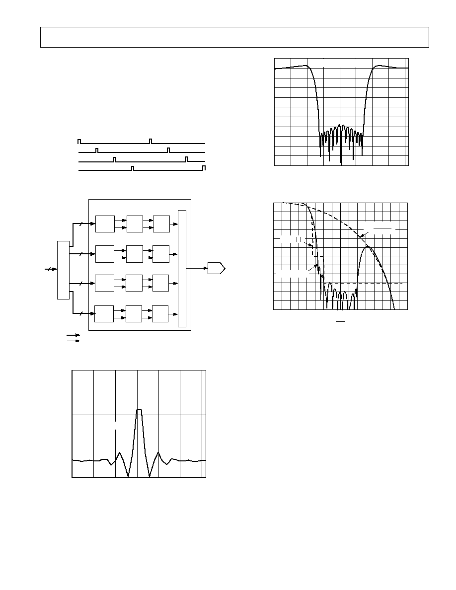
AD6622
27
REV. 0
Driving Multiple TSP Serial Ports
When properly configured, the AD6622 will drive each SDFS
out of phase. Each new piece of data should be driven only into
the TSP that pulses its SDFS pin at that time.
In the UMTS example, L = 64 and N
TSP
= 4, so each serial port
need only accept every 4th
input sample. Each serial port is
shifting at peak capacity, so sample 1, 2, and 3 begin shifting
into Serial Ports B, C, and D before Sample 0 is completed into
Serial Port A.
0
1
2
3
4
5
6
7
SDFSA
SDFSB
SDFSC
SDFSD
Figure 21. SDFS Timing for WBCDMA
RAM
COEF
FILTER
CIC
NCO
I
Q
8.196MSPS 65.536MSPS
SUMMATION
DATA
REFORMATTER
4.096
MCPS
1.024
MCPS
32
1.024
MCPS
32
1.024
MCPS
1.024
MCPS
65.536
MSPS
DAC
COMPLEX SIGNAL 32 BITS (16 I, 16 Q)
REAL OR IMAGINARY SIGNAL
AD6622
32
32
32
RAM
COEF
FILTER
CIC
NCO
I
Q
8.196MSPS 65.536MSPS
RAM
COEF
FILTER
CIC
NCO
I
Q
8.196MSPS 65.536MSPS
RAM
COEF
FILTER
CIC
NCO
I
Q
8.196MSPS 65.536MSPS
Figure 22. Block Diagram for WBCDMA
0
5
10
15
20
0
0.5
1.0
25
30
COEF J
Figure 23. Typical Impulse Response for WBCDMA
70
dBc
60
50
40
30
20
10
0
10
100
90
80
RAM COEFFICIENT FILTER
0
1000
2000
3000
4000
5000
6000
7000
8000
kHz
Figure 24. Typical FIR Frequency Response for WBCDMA
70
dBc
60
50
40
30
20
10
0
100
90
80
0 0.5 1.0 1.5 2.0 2.5 3.0 3.5 4.0
110
120
dB(AD6624(f))
dB
(
)
H
CIC
(f)
LEVEL
5
SPEC( f )
4.5 5.0 5.5 6.0 6.5 7.0 7.5 8.0
f
MHz
Figure 25. Typical Composite Frequency Response for
WBCDMA
THERMAL MANAGEMENT
The power dissipation of the AD6622 is primarily determined
by three factors: the clock rate, the number of channels active,
and the distribution of interpolation rates. The faster the clock
rate the more power dissipated by the CMOS structures of
the AD6622; the more channels active, the higher the overall
power of the chip. Low interpolation rates in the CIC stages
(CIC5, CIC2) results in higher power dissipation. All these factors
should be analyzed as each application has different thermal
requirements.
The AD6622 128-lead MQFP is specially designed to provide
excellent thermal performance. To achieve the best performance,
the power and ground leads should be connected directly to
planes on the PC board. This provides the best thermal transfer
from the AD6622 to the PC board.
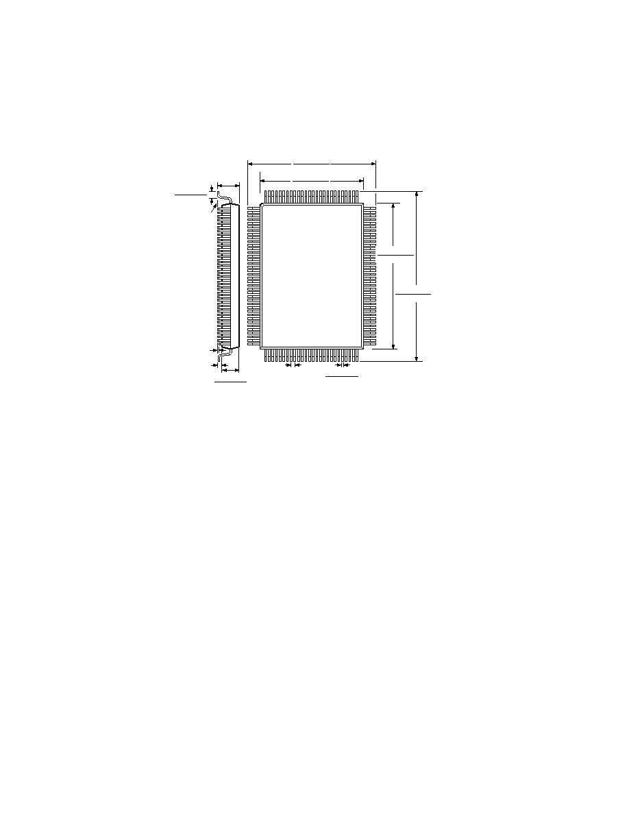
28
C377285/00 (rev. 0) 00968
PRINTED IN U.S.A.
AD6622
REV. 0
OUTLINE DIMENSIONS
Dimensions shown in inches and (mm).
128-Lead MQFP (Metric Quad Flatpack)
(S-128A)
TOP VIEW
(PINS DOWN)
1
38
39
65
64
102
128
103
0.011 (0.27)
0.007 (0.17)
0.020 (0.50)
BSC
0.555 (14.10)
0.547 (13.90)
0.685 (17.40)
0.669 (17.00)
0.791 (20.10)
0.783 (19.90)
0.921 (23.40)
0.906 (23.00)
0.041 (1.03)
0.031 (0.78)
SEATING
PLANE
0.134 (3.40)
MAX
0.003 (0.08)
MAX
0.010 (0.25)
MIN
0.110 (2.80)
0.102 (2.60)