 | ÐлекÑÑоннÑй компоненÑ: AD6623ABC | СкаÑаÑÑ:  PDF PDF  ZIP ZIP |
Äîêóìåíòàöèÿ è îïèñàíèÿ www.docs.chipfind.ru
REV. 0
Information furnished by Analog Devices is believed to be accurate and
reliable. However, no responsibility is assumed by Analog Devices for its
use, nor for any infringements of patents or other rights of third parties that
may result from its use. No license is granted by implication or otherwise
under any patent or patent rights of Analog Devices.
a
AD6623
One Technology Way, P.O. Box 9106, Norwood, MA 02062-9106, U.S.A.
Tel: 781/329-4700
www.analog.com
Fax: 781/326-8703
© Analog Devices, Inc., 2002
4-Channel, 104 MSPS Digital
Transmit Signal Processor (TSP)
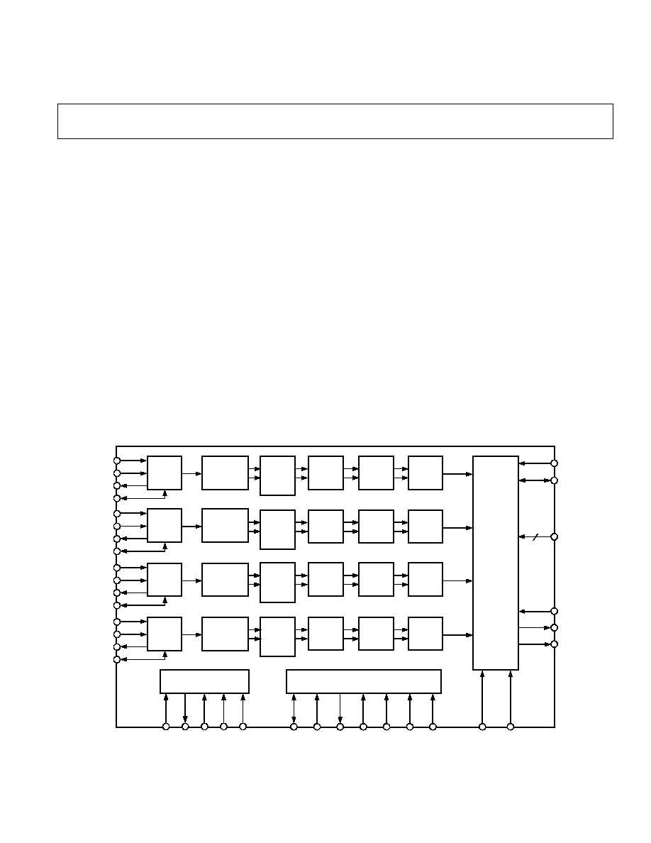
FUNCTIONAL BLOCK DIAGRAM
SP
ORT
RAM
COEFFICIENT
FILTER
DATA
SCALER
AND
POWER
RAMP
CIC5
FILTER
RCIC2
FILTER
NCO
I
Q
CHAN A
I
Q
I
Q
I
Q
JTAG
CS
A[2:0]
MODE
RW
DTACK
DS
D[7:0]
IN
QIN
SYNC
OEN
QOUT
OUT
[17:0]
SDINA
SDFIA
SDFOA
SCLKA
SDINB
SDFIB
SDFOB
SCLKB
SDINC
SDFIC
SDFOC
SCLKC
SDIND
SDFID
SCLKD
SDFOD
SUMMATION
SCALER
AND
POWER
RAMP
CIC5
FILTER
RCIC2
FILTER
NCO
I
Q
CHAN B
I
Q
I
Q
I
Q
SCALER
AND
POWER
RAMP
CIC5
FILTER
RCIC2
FILTER
NCO
I
Q
CHAN C
I
Q
I
Q
I
Q
SCALER
AND
POWER
RAMP
CIC5
FILTER
RCIC2
FILTER
NCO
I
Q
CHAN D
I
Q
I
Q
I
Q
MICROPORT
CLK
RESET
4
[170]
SP
ORT
RAM
COEFFICIENT
FILTER
DATA
SP
ORT
RAM
COEFFICIENT
FILTER
DATA
SP
ORT
RAM
COEFFICIENT
FILTER
DATA
NCO = NUMERICALLY CONTROLLED
OSCILLATOR/TUNER
TDL
TMS TCK
TRST
TDO
FEATURES
Pin Compatible to the AD6622
18-Bit Parallel Digital IF Output
Real or Interleaved Complex
18-Bit Bidirectional Parallel Digital IF Input/Output
Allows Cascade of Chips for Additional Channels
Clipped or Wrapped Over Range
Two's Complement or Offset Binary Output
Four Independent Digital Transmitters in Single Package
RAM Coefficient Filter (RCF)
Programmable IF and Modulation for Each Channel
Programmable Interpolating RAM Coefficient Filter
p/4-DQPSK Differential Phase Encoder
3p/8-PSK Linear Encoder
8-PSK Linear Encoder
Programmable GMSK Look-Up Table
Programmable QPSK Look-Up Table
All-Pass Phase Equalizer
Programmable Fine Scaler
Programmable Power Ramp Unit
High Speed CIC Interpolating Filter
Digital Resampling for Noninteger Interpolation Rates
NCO Frequency Translation
Spurious Performance Better than 100 dBc
Separate 3-Wire Serial Data Input for Each Channel
Bidirectional Serial Clocks and Frames
Microprocessor Control
2.5 V CMOS Core, 3.3 V Outputs, 5 V Inputs
JTAG Boundary Scan
APPLICATIONS
Cellular/PCS Base Stations
Micro/Pico Cell Base Stations
Wireless Local Loop Base Stations
Multicarrier, Multimode Digital Transmit
GSM, EDGE, IS136, PHS, IS95, TDS CDMA, UMTS,
CDMA2000
Phased Array Beam Forming Antennas
Software Defined Radio
Tuning Resolution Better than 0.025 Hz
Real or Complex Outputs

REV. 0
AD6623
2
TABLE OF CONTENTS
FEATURES . . . . . . . . . . . . . . . . . . . . . . . . . . . . . . . . . . . . . . . . . . . . . . . 1
APPLICATIONS . . . . . . . . . . . . . . . . . . . . . . . . . . . . . . . . . . . . . . . . . . . 1
FUNCTIONAL BLOCK DIAGRAM . . . . . . . . . . . . . . . . . . . . . . . . . . . 1
PRODUCT DESCRIPTION . . . . . . . . . . . . . . . . . . . . . . . . . . . . . . . . . . 3
FUNCTIONAL OVERVIEW . . . . . . . . . . . . . . . . . . . . . . . . . . . . . . . . . . 3
RECOMMENDED OPERATING CONDITIONS . . . . . . . . . . . . . . . . 4
ELECTRICAL CHARACTERISTICS . . . . . . . . . . . . . . . . . . . . . . . . . . 4
LOGIC INPUTS (5 V TOLERANT) . . . . . . . . . . . . . . . . . . . . . . . . . 4
LOGIC OUTPUTS . . . . . . . . . . . . . . . . . . . . . . . . . . . . . . . . . . . . . . . 4
IDD SUPPLY CURRENT . . . . . . . . . . . . . . . . . . . . . . . . . . . . . . . . . . 4
POWER DISSIPATION . . . . . . . . . . . . . . . . . . . . . . . . . . . . . . . . . . . 4
GENERAL TIMING CHARACTERISTICS . . . . . . . . . . . . . . . . . . . . . 5
MICROPROCESSOR PORT TIMING CHARACTERISTICS . . . . . . . . 6
MICROPROCESSOR PORT, MODE INM (MODE = 0) . . . . . . . . . 6
MICROPROCESSOR PORT, MOTOROLA (MODE = 1) . . . . . . . . 6
TIMING DIAGRAMS . . . . . . . . . . . . . . . . . . . . . . . . . . . . . . . . . . . . . 79
ABSOLUTE MAXIMUM RATINGS . . . . . . . . . . . . . . . . . . . . . . . . . . 10
THERMAL CHARACTERISTICS . . . . . . . . . . . . . . . . . . . . . . . . . . . . 10
EXPLANATION OF TEST LEVELS . . . . . . . . . . . . . . . . . . . . . . . . . . 10
ORDERING GUIDE . . . . . . . . . . . . . . . . . . . . . . . . . . . . . . . . . . . . . . . 10
ESD SENSITIVITY . . . . . . . . . . . . . . . . . . . . . . . . . . . . . . . . . . . . . . . . 10
PIN CONFIGURATION 128-Lead MQFP . . . . . . . . . . . . . . . . . . . . 11
128 PIN FUNCTION DESCRIPTION . . . . . . . . . . . . . . . . . . . . . . . 12
PIN CONFIGURATION 196-Lead BGA . . . . . . . . . . . . . . . . . . . . . . 13
196 PIN FUNCTION DESCRIPTION . . . . . . . . . . . . . . . . . . . . . . . 14
POWER SUPPLY . . . . . . . . . . . . . . . . . . . . . . . . . . . . . . . . . . . . . . . 14
INPUTS . . . . . . . . . . . . . . . . . . . . . . . . . . . . . . . . . . . . . . . . . . . . . . . 14
CONTROL . . . . . . . . . . . . . . . . . . . . . . . . . . . . . . . . . . . . . . . . . . . . . 14
MICROPORT CONTROL . . . . . . . . . . . . . . . . . . . . . . . . . . . . . . . . 14
OUTPUTS . . . . . . . . . . . . . . . . . . . . . . . . . . . . . . . . . . . . . . . . . . . . . 14
JTAG AND BIST . . . . . . . . . . . . . . . . . . . . . . . . . . . . . . . . . . . . . . . . 14
SERIAL DATA PORT . . . . . . . . . . . . . . . . . . . . . . . . . . . . . . . . . . . . . . 15
Serial Master Mode (SCS = 0) . . . . . . . . . . . . . . . . . . . . . . . . . . . . . . 15
Serial Slave Mode (SCS = 1) . . . . . . . . . . . . . . . . . . . . . . . . . . . . . . . 15
Self-Framing Mode . . . . . . . . . . . . . . . . . . . . . . . . . . . . . . . . . . . . . . . 15
External Framing Mode . . . . . . . . . . . . . . . . . . . . . . . . . . . . . . . . . . . 15
Serial Port Cascade Configuration . . . . . . . . . . . . . . . . . . . . . . . . . . . 15
Serial Data Format . . . . . . . . . . . . . . . . . . . . . . . . . . . . . . . . . . . . . . . 15
PROGRAMMABLE RAM COEFFICIENT FILTER (RCF) . . . . . . . . . 16
OVERVIEW OF THE RCF BLOCKS . . . . . . . . . . . . . . . . . . . . . . . . 16
INTERPOLATING FIR FILTER . . . . . . . . . . . . . . . . . . . . . . . . . . . 17
RCF CONTROL REGISTERS . . . . . . . . . . . . . . . . . . . . . . . . . . . . . 19
PSK MODULATOR . . . . . . . . . . . . . . . . . . . . . . . . . . . . . . . . . . . . . 19
/4-DQSPK MODULATION . . . . . . . . . . . . . . . . . . . . . . . . . . . . 20
8-PSK MODULATION . . . . . . . . . . . . . . . . . . . . . . . . . . . . . . . . . 20
3 /8-8-PSK MODULATION . . . . . . . . . . . . . . . . . . . . . . . . . . . . 20
MSK Look-Up Table . . . . . . . . . . . . . . . . . . . . . . . . . . . . . . . . . . . . . 21
GMSK Look-Up Table . . . . . . . . . . . . . . . . . . . . . . . . . . . . . . . . . . . . 21
QPSK Look-Up Table . . . . . . . . . . . . . . . . . . . . . . . . . . . . . . . . . . . . 21
PHASE EQUALIZER . . . . . . . . . . . . . . . . . . . . . . . . . . . . . . . . . . . . 21
SCALE AND RAMP . . . . . . . . . . . . . . . . . . . . . . . . . . . . . . . . . . . . . 21
FINE SCALING . . . . . . . . . . . . . . . . . . . . . . . . . . . . . . . . . . . . . . . . . . . 21
RCF POWER RAMPING . . . . . . . . . . . . . . . . . . . . . . . . . . . . . . . . . . . 21
CASCADED INTERGRATOR COMB (CIC)
INTERPOLATING FILTERS . . . . . . . . . . . . . . . . . . . . . . . . . . . . . . . . 21
CIC Scaling . . . . . . . . . . . . . . . . . . . . . . . . . . . . . . . . . . . . . . . . . . . . . 22
CIC5 . . . . . . . . . . . . . . . . . . . . . . . . . . . . . . . . . . . . . . . . . . . . . . . . . . 22
rCIC2 . . . . . . . . . . . . . . . . . . . . . . . . . . . . . . . . . . . . . . . . . . . . . . . . . 23
NUMERICALLY CONTROLLED
OSCILLATOR/TUNER (NCO) . . . . . . . . . . . . . . . . . . . . . . . . . . . . . . . . 24
Phase Dither . . . . . . . . . . . . . . . . . . . . . . . . . . . . . . . . . . . . . . . . . . . . 25
Amplitude Dither . . . . . . . . . . . . . . . . . . . . . . . . . . . . . . . . . . . . . . . . 25
Phase Offset . . . . . . . . . . . . . . . . . . . . . . . . . . . . . . . . . . . . . . . . . . . . 25
NCO Frequency Update and Phase Offset Update
Hold-Off Counters . . . . . . . . . . . . . . . . . . . . . . . . . . . . . . . . . . . . . . . 25
NCO Control Scale . . . . . . . . . . . . . . . . . . . . . . . . . . . . . . . . . . . . . . . 25
SUMMATION BLOCK . . . . . . . . . . . . . . . . . . . . . . . . . . . . . . . . . . . . . 25
SYNCHRONIZATION . . . . . . . . . . . . . . . . . . . . . . . . . . . . . . . . . . . . . 26
Start . . . . . . . . . . . . . . . . . . . . . . . . . . . . . . . . . . . . . . . . . . . . . . . . . . 26
Start with No Sync . . . . . . . . . . . . . . . . . . . . . . . . . . . . . . . . . . . . . . . 26
Start with Soft Sync . . . . . . . . . . . . . . . . . . . . . . . . . . . . . . . . . . . . . . 27
Start with Pin Sync . . . . . . . . . . . . . . . . . . . . . . . . . . . . . . . . . . . . . . . 27
Hop with Soft Sync . . . . . . . . . . . . . . . . . . . . . . . . . . . . . . . . . . . . . . . 27
Hop with Pin Sync . . . . . . . . . . . . . . . . . . . . . . . . . . . . . . . . . . . . . . . 27
Beam with Soft Sync . . . . . . . . . . . . . . . . . . . . . . . . . . . . . . . . . . . . . . 28
Beam with Pin Sync . . . . . . . . . . . . . . . . . . . . . . . . . . . . . . . . . . . . . . 28
JTAG INTERFACE . . . . . . . . . . . . . . . . . . . . . . . . . . . . . . . . . . . . . . . . 28
SCALING . . . . . . . . . . . . . . . . . . . . . . . . . . . . . . . . . . . . . . . . . . . . . . . . 28
Multicarrier Scaling . . . . . . . . . . . . . . . . . . . . . . . . . . . . . . . . . . . . . . 28
Single Carrier Scaling . . . . . . . . . . . . . . . . . . . . . . . . . . . . . . . . . . . . . 29
MICROPORT INTERFACE . . . . . . . . . . . . . . . . . . . . . . . . . . . . . . . . . 29
MicroPort Control . . . . . . . . . . . . . . . . . . . . . . . . . . . . . . . . . . . . . . 29
EXTERNAL MEMORY MAP . . . . . . . . . . . . . . . . . . . . . . . . . . . . . . . . 29
Intel Nonmultiplexed Mode (INM) . . . . . . . . . . . . . . . . . . . . . . . . . . 30
Motorola Nonmultiplexed Mode (MNM) . . . . . . . . . . . . . . . . . . . . . 30
External Address 7 Upper Address Register (UAR) . . . . . . . . . . . . . . 30
External Address 6 Lower Address Register (LAR) . . . . . . . . . . . . . . 30
External Address 5 Sync . . . . . . . . . . . . . . . . . . . . . . . . . . . . . . . . . . . 30
External Address 4 Sleep . . . . . . . . . . . . . . . . . . . . . . . . . . . . . . . . . . 31
External Address 3:0 (Data Bytes) . . . . . . . . . . . . . . . . . . . . . . . . . . . 31
INTERNAL CONTROL REGISTERS AND ON-CHIP RAM . . . . . . . . . 31
AD6623 and AD6622 Compatibility
Common Function Registers (not associated
with a particular channel) . . . . . . . . . . . . . . . . . . . . . . . . . . . . . . . . 31
Channel Function Registers (0x1XX = Ch. A,
0x2XX = Ch. B, 0x3XX = Ch. C, 0x4XX = Ch. D) . . . . . . . . . . . 31
(0x000) Summation Mode Control . . . . . . . . . . . . . . . . . . . . . . . . . . 33
(0x001) Sync Mode Control . . . . . . . . . . . . . . . . . . . . . . . . . . . . . . . . 33
(0x002) BIST Counter . . . . . . . . . . . . . . . . . . . . . . . . . . . . . . . . . . . . 33
(0x003) BIST Result . . . . . . . . . . . . . . . . . . . . . . . . . . . . . . . . . . . . . . 33
Channel Function Registers . . . . . . . . . . . . . . . . . . . . . . . . . . . . . . . . 34
(0xn00) Start Update Hold-Off Counter . . . . . . . . . . . . . . . . . . . . . . 34
(0xn01) NCO Control . . . . . . . . . . . . . . . . . . . . . . . . . . . . . . . . . . . . 34
(0xn02) NCO Frequency . . . . . . . . . . . . . . . . . . . . . . . . . . . . . . . . . . 34
(0xn03) NCO Frequency Update Hold-Off Counter . . . . . . . . . . . . . 34
(0xn04) NCO Phase Offset . . . . . . . . . . . . . . . . . . . . . . . . . . . . . . . . . 34
(0xn05) NCO Phase Offset Update Hold-Off Counter . . . . . . . . . . . . 34
(0xn06) CIC Scale . . . . . . . . . . . . . . . . . . . . . . . . . . . . . . . . . . . . . . . 34
(0xn07) CIC2 Decimation 1 (M
CIC2
1) . . . . . . . . . . . . . . . . . . . . . 34
(0xn08) CIC2 Interpolation 1 (L
CIC2
1) . . . . . . . . . . . . . . . . . . . . 34
(0xn09) CIC5 Interpolation . . . . . . . . . . . . . . . . . . . . . . . . . . . . . . . . 34
(0xn0A) Number of RCF Coefficients 1 . . . . . . . . . . . . . . . . . . . . . 34
(0xn0B) RCF Coefficient Offset . . . . . . . . . . . . . . . . . . . . . . . . . . . . . 34
(0xn0C) Channel Mode Control 1 . . . . . . . . . . . . . . . . . . . . . . . . . . . 34
(0xn0D) Channel Mode Control 2 . . . . . . . . . . . . . . . . . . . . . . . . . . . 35
(0xn0E) Fine Scale Factor . . . . . . . . . . . . . . . . . . . . . . . . . . . . . . . . . 35
(0xn0F) RCF Time Slot Hold-Off Counter . . . . . . . . . . . . . . . . . . . . 35
(0xn100xn11) RCF Phase Equalizer Coefficients . . . . . . . . . . . . . . . 35
(0xn120xn15) FIR-PSK Magnitudes . . . . . . . . . . . . . . . . . . . . . . . . 35
(0xn16) Serial Port Setup . . . . . . . . . . . . . . . . . . . . . . . . . . . . . . . . . . 35
(0xn17) Power Ramp Length 0 . . . . . . . . . . . . . . . . . . . . . . . . . . . . . . 35
(0xn18) Power Ramp Length 1 . . . . . . . . . . . . . . . . . . . . . . . . . . . . . . 35
(0xn19) Power Ramp Rest Time . . . . . . . . . . . . . . . . . . . . . . . . . . . . . 35
(0xn200xn1F) Unused . . . . . . . . . . . . . . . . . . . . . . . . . . . . . . . . . . . 35
(0xn200xn3F) Data Memory . . . . . . . . . . . . . . . . . . . . . . . . . . . . . . 35
(0xn400xn17F) Power Ramp Coefficient Memory . . . . . . . . . . . . . . 35
Pseudocode . . . . . . . . . . . . . . . . . . . . . . . . . . . . . . . . . . . . . . . . . . . . . 35
Write Pseudocode . . . . . . . . . . . . . . . . . . . . . . . . . . . . . . . . . . . . . . 35
Read Pseudocode . . . . . . . . . . . . . . . . . . . . . . . . . . . . . . . . . . . . . . 36
APPLICATIONS . . . . . . . . . . . . . . . . . . . . . . . . . . . . . . . . . . . . . . . . . . 36
USING THE AD6623 TO PROCESS UMTS CARRIERS . . . . . . . . 36
DIGITAL-TO-ANALOG CONVERTER (DAC) SELECTION . . . . . . . 36
MULTIPLE TSP OPERATION . . . . . . . . . . . . . . . . . . . . . . . . . . . . 36
Determining the Number of TSPs to Use . . . . . . . . . . . . . . . . . . . . 36
Programming Mulitple TSPs . . . . . . . . . . . . . . . . . . . . . . . . . . . . . 37
Driving Multiple TSP Serial Ports . . . . . . . . . . . . . . . . . . . . . . . . . 37
THERMAL MANAGEMENT . . . . . . . . . . . . . . . . . . . . . . . . . . . . . . 38
PACKAGE OUTLINE DIMENSIONS . . . . . . . . . . . . . . . . . . . . . . . . . 39

REV. 0
AD6623
3
PRODUCT DESCRIPTION
The AD6623 is a 4-channel Transmit Signal Processor (TSP)
that creates high bandwidth data for Transmit Digital-to-Analog
Converters (TxDACs) from baseband data provided by a Digital
Signal Processor (DSP). Modern TxDACs have achieved suffi-
ciently high sampling rates, analog bandwidth, and dynamic range
to create the first Intermediate Frequency (IF) directly. The
AD6623 synthesizes multicarrier and multistandard digital signals
to drive these TxDACs. The RAM-based architecture allows easy
reconfiguration for multimode applications. Modulation, pulse-
shaping and anti-imaging filters, static equalization, and tuning
functions are combined in a single, cost-effective device. Digital
IF signal processing provides repeatable manufacturing, higher
accuracy, and more flexibility than comparable high dynamic
range analog designs.
The AD6623 has four identical digital TSPs complete with synchro-
nization circuitry and cascadable wideband channel summation.
AD6623 is pin compatible to AD6622 and can operate in AD6622-
compatible control register mode.
The AD6623 utilizes a 3.3 V I/O power supply and a 2.5 V core
power supply. All I/O pins are 5 V tolerant. All control registers
and coefficient values are programmed through a generic micro-
processor interface. Intel and Motorola microprocessor bus modes
are supported. All inputs and outputs are LVCMOS compatible.
FUNCTIONAL OVERVIEW
Each TSP has five cascaded signal processing elements: a pro-
grammable interpolating RAM Coefficient Filter (RCF), a
programmable Scale and Power Ramp, a programmable fifth order
Cascaded Integrator Comb (CIC5) interpolating filter, a flexible
second order Resampling Cascaded Integrator Comb filter (rCIC2),
and a Numerically Controlled Oscillator/Tuner (NCO).
The outputs of the four TSPs are summed and scaled on-chip.
In multicarrier wideband transmitters, a bidirectional bus allows
the Parallel (wideband) IF Input/Output to drive a second DAC.
In this operational mode two AD6623 channels drive one DAC
and the other two AD6623 channels drive a second DAC. Mul-
tiple AD6623s may be combined by driving the INOUT[17:0] of
the succeeding with the OUT[17:0] of the preceding chip. The
INOUT[17:0] can alternatively be masked off by software to
allow preceding AD6623's outputs to be ignored.
Each channel accepts input data from independent serial ports
that may be connected directly to the serial port of Digital Signal
Processor (DSP) chips.
The RCF implements any one of the following functions:
Interpolating Finite Impulse Response (FIR) filter, /4-DQPSK
modulator, 8-PSK modulator, or 3 /8-8-PSK modulator, GMSK
modulator, and QPSK modulator. Each AD6623 channel can
be dynamically switched between the GMSK modulation mode
and the 3 /8-8-PSK modulation mode in order to support the
GSM/EDGE standard. The RCF also implements an Allpass
Phase Equalizer (APE) which meets the requirements of IS-95-A/B
standard (CDMA transmission).
The programmable Scale and Power Ramp block allows power
ramping on a time-slot basis as specified for some air-interface
standards (e.g., GSM, EDGE). A fine scaling unit at the pro-
grammable FIR filter output allows an easy signal amplitude
level adjustment on time slot basis.
The CIC5 provides integer rate interpolation from 1 to 32 and
coarse anti-image filtering. The rCIC2 provides fractional rate
interpolation from 1 to 4096 in steps of 1/512. The wide range
of interpolation factors in each CIC filter stage and a highly
flexible resampler incorporated into rCIC2 makes the AD6623
useful for creating both narrowband and wideband carriers in a
high-speed sample stream.
The high resolution 32-bit NCO allows flexibility in frequency
planning and supports both digital and analog air interface stan-
dards. The high speed NCO tunes the interpolated complex signal
from the rCIC2 to an IF channel. The result may be real or com-
plex. Multicarrier phase synchronization pins and phase offset
registers allow intelligent management of the relative phase of
independent RF channels. This capability supports the require-
ments for phased array antenna architectures and management
of the wideband peak/power ratio to minimize clipping at the DAC.
The wideband Output Ports can deliver real or complex data.
Complex words are interleaved into real (I) and imaginary (Q)
parts at half the master clock rate.

REV. 0
4
AD6623
RECOMMENDED OPERATING CONDITIONS
Test
AD6623
Parameter
Level
Min
Typ
Max
Unit
VDD
IV
2.25
2.5
2.75
V
VDDIO
IV
3.0
3.3
3.6
V
T
AMBIENT
IV
40
+25
+70
°C
ELECTRICAL CHARACTERISTICS
Parameter (Conditions)
Temp
Test Level
Min
Typ
Max
Unit
LOGIC INPUTS (5 V TOLERANT)
Logic Compatibility
Full
3.3 V CMOS
Logic "1" Voltage
Full
IV
2.0
5.0
V
Logic "0" Voltage
Full
IV
0.3
+0.8
V
Logic "1" Current
Full
IV
1
10
µA
Logic "0" Current
Full
IV
0
10
µA
Input Capacitance
25
°C
V
4
pF
LOGIC OUTPUTS
Logic Compatibility
Full
3.3 V CMOS/TTL
Logic "1" Voltage (I
OH
= 0.25 mA)
Full
IV
2.0
VDD 0.2
V
Logic "0" Voltage (I
OL
= 0.25 mA)
Full
IV
0.2
0.4
V
IDD SUPPLY CURRENT
CLK = 104 MHz, VDD = 2.75 V
*
Full
IV
422
TBD
*
mA
CLK = 104 MHz, VDDIO = 3.6 V
*
Full
IV
193
mA
GSM Example: CORE
V
232
mA
I/O
56
mA
IS-136 Example: CORE
V
207
mA
I/O
55
mA
WBCDMA Example
V
Tbd
mA
Sleep Mode
Full
IV
Tbd
TBD
mA
POWER DISSIPATION
GSM Example
V
740
mW
IS-136 Example
V
700
mW
WBCDMA Example
V
Tbd
mW
Sleep Mode
Full
IV
Tbd
TBD
mW
*This specification denotes an absolute maximum supply current for the device. The conditions include all channels active, minimum interpolation in both CIC
stages, and maximum switching of input data. In an actual application the power will be less.
See the Thermal Management section of the data sheet for further details.

REV. 0
5
AD6623
GENERAL TIMING CHARACTERISTICS
1, 2
Test
AD6623AS
Parameter (Conditions)
Temp
Level
Min
Typ
Max
Unit
CLK Timing Requirements:
t
CLK
CLK Period
Full
I
9.6
ns
t
CLKL
CLK Width Low
Full
IV
3
ns
t
CLKH
CLK Width High
Full
IV
3
0.5
× t
CLK
ns
RESET Timing Requirement:
t
RESL
RESET Width Low
Full
I
30.0
ns
Input Data Timing Requirements:
t
SI
INOUT[17:0], QIN to
CLK Setup Time
Full
IV
1
ns
t
HI
INOUT[17:0], QIN to
CLK Hold Time
Full
IV
2
ns
Output Data Timing Characteristics:
t
DO
CLK to OUT[17:0], INOUT[17:0],
QOUT Output Delay Time
Full
IV
2
6
ns
t
DZO
OEN HIGH to OUT[17:0] Active
Full
IV
3
7.5
ns
SYNC Timing Requirements:
t
SS
SYNC(0, 1, 2, 3) to
CLK Setup Time
Full
IV
1
ns
t
HS
SYNC(0, 1, 2, 3) to
CLK Hold Time
Full
IV
2
ns
Master Mode Serial Port Timing Requirements (SCS = 0):
Switching Characteristics
3
t
DSCLK1
CLK to SCLK Delay (divide by 1)
Full
IV
4
10.5
ns
t
DSCLKH
CLK to SCLK Delay (for any other divisor) Full
IV
5
13
ns
t
DSCLKL
CLK to SCLK Delay
(divide by 2 or even number)
Full
IV
3.5
9
ns
t
DSCLKLL
CLK to SCLK Delay
(divide by 3 or odd number)
Full
IV
4
10
ns
Channel is Self-Framing
t
SSDI0
SDIN to
SCLK Setup Time
Full
IV
1.7
ns
t
HSDI0
SDIN to
SCLK Hold Time
Full
IV
0
ns
t
DSFO0A
SCLK to SDFO Delay
Full
IV
0.5
3.5
ns
Channel is External-Framing
t
SSFI0
SDFI to
SCLK Setup Time
Full
IV
2
ns
t
HSFI0
SDFI to
SCLK Hold Time
Full
IV
0
ns
t
SSDI0
SDIN to
SCLK Setup Time
Full
IV
2
ns
t
HSDI0
SDIN to
SCLK Hold Time
Full
IV
0
ns
t
DSFO0B
SCLK to SDFO Delay
Full
IV
0.5
3
ns
Slave Mode Serial Port Timing Requirements (SCS = 1):
Switching Characteristics
3
t
SCLK
SCLK Period
Full
IV
2 t
CLK
ns
t
SCLKL
SCLK Low Time
Full
IV
3.5
ns
t
SCLKH
SCLK High Time
Full
IV
3.5
ns
Channel is Self-Framing
t
SSDH
SDIN to
SCLK Setup Time
Full
IV
1
ns
t
HSDH
SDIN to
SCLK Hold Time
Full
IV
2.5
ns
t
DSFO1
SCLK to SDFO Delay
Full
IV
4
10
ns
Channel is External-Framing
t
SSFI1
SDFI to
SCLK Setup Time
Full
IV
2
ns
t
HSFI1
SDFI to
SCLK Hold Time
Full
IV
1
ns
t
SSDI1
SDIN to
SCLK Setup Time
Full
IV
1
ns
t
HSDI1
SDIN to
SCLK Hold Time
Full
IV
2.5
ns
t
DSFO1
SCLK to SDFO Delay
Full
IV
10
ns
NOTES
1
All Timing Specifications valid over VDD range of 2.375 V to 2.675 V and VDDIO range of 3.0 V to 3.6 V.
2
C
LOAD
= 40 pF on all outputs (unless otherwise specified).
3
The timing parameters for SCLK, SDIN, SDFI, SDFO, and SYNC apply to all four channels (A, B, C, and D).
Specifications subject to change without notice.

REV. 0
6
AD6623
MICROPROCESSOR PORT TIMING CHARACTERISTICS
1, 2
Test
AD6623AS
Parameter (Conditions)
Temp
Level
Min
Typ
Max
Unit
MICROPROCESSOR PORT, MODE INM (MODE = 0)
MODE INM Write Timing:
t
SC
Control
3
to
CLK Setup Time
Full
IV
4.5
ns
t
HC
Control
3
to
CLK Hold Time
Full
IV
2.0
ns
t
HWR
WR(RW) to RDY(DTACK) Hold Time
Full
IV
8.0
ns
t
SAM
Address/Data to
WR(RW) Setup Time
Full
IV
3.0
ns
t
HAM
Address/Data to RDY(
DTACK) Hold Time
Full
IV
2.0
ns
t
DRDY
WR(RW) to RDY(DTACK) Delay
Full
IV
4.0
ns
t
ACC
WR(RW) to RDY(DTACK) High Delay
Full
IV
4
× t
CLK
5
× t
CLK
9
× t
CLK
ns
MODE INM Read Timing:
t
SC
Control
3
to
CLK Setup Time
Full
IV
4.5
ns
t
HC
Control
3
to
CLK Hold Time
Full
IV
2.0
ns
t
SAM
Address to
RD(DS) Setup Time
Full
IV
3.0
ns
t
HAM
Address to Data Hold Time
Full
IV
2.0
ns
t
ZOZ
Data Three-State Delay
Full
IV
ns
t
DD
RDY(
DTACK) to Data Delay
Full
IV
ns
t
DRDY
RD(DS) to RDY(DTACK) Delay
Full
IV
4.0
ns
t
ACC
RD(DS) to RDY(DTACK) High Delay
Full
IV
8
× t
CLK
10
× t
CLK
13
× t
CLK
ns
MICROPROCESSOR PORT, MOTOROLA (MODE = 1)
MODE MNM Write Timing:
t
SC
Control
3
to
CLK Setup Time
Full
IV
4.5
ns
t
HC
Control
3
to
CLK Hold Time
Full
IV
2.0
ns
t
HDS
DS(RD) to DTACK(RDY) Hold Time
Full
IV
8.0
ns
t
HRW
RW(
WR) to DTACK(RDY) Hold Time
Full
IV
8.0
ns
t
SAM
Address/Data to RW(
WR) Setup Time
Full
IV
3.0
ns
t
HAM
Address/Data to RW(
WR) Hold Time
Full
IV
2.0
ns
t
DDTACK
DS(RD) to DTACK(RDY) Delay
ns
t
ACC
RW(
WR) to DTACK(RDY) Low Delay
Full
IV
4
× t
CLK
5
× t
CLK
9
× t
CLK
ns
MODE MNM Read Timing:
t
SC
Control
3
to
CLK Setup Time
Full
IV
4.0
ns
t
HC
Control
3
to
CLK Hold Time
Full
IV
2.0
ns
t
HDS
DS(RD) to DTACK(RDY) Hold Time
Full
IV
8.0
ns
t
SAM
Address to
DS(RD) Setup Time
Full
IV
3.0
ns
t
HAM
Address to Data Hold Time
Full
IV
2.0
ns
t
ZD
Data Three-State Delay
Full
IV
ns
t
DD
DTACK(RDY) to Data Delay
Full
IV
ns
t
DDTACK
DS(RD) to DTACK(RDY) Delay
Full
IV
ns
t
ACC
DS(RD) to DTACK(RDY) Low Delay
Full
IV
8
× t
CLK
10
× t
CLK
13
× t
CLK
ns
NOTES
1
All Timing Specifications valid over VDD range of 2.375 V to 2.675 V and VDDIO range of 3.0 V to 3.6 V.
2
C
LOAD
= 40 pF on all outputs (unless otherwise specified).
3
Specification pertains to control signals: RW, (
WR), DS, (RD), CS.
Specifications subject to change without notice.
REV. 0
AD6623
7
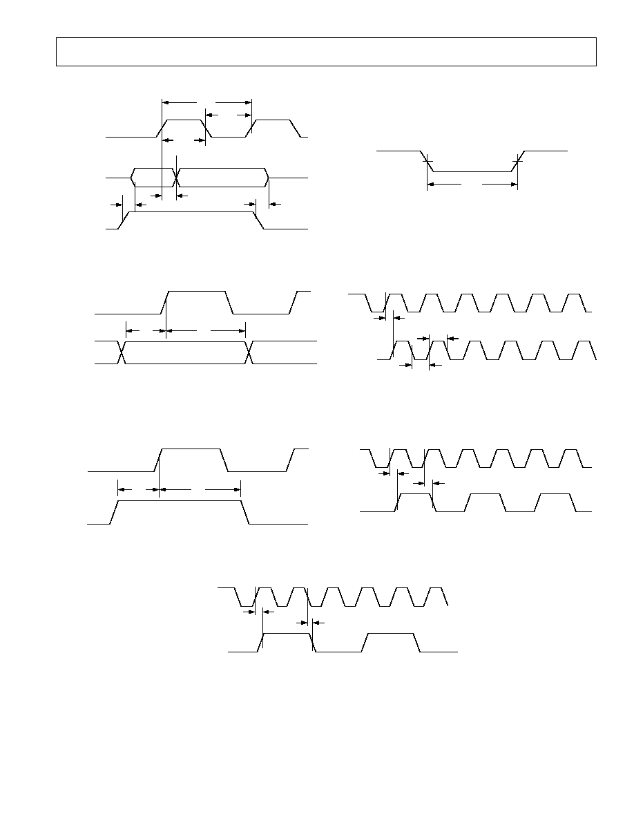
TIMING DIAGRAMS
CLK
t
DO
t
CLK
t
CLKL
t
CLKH
t
ZO
t
ZO
OEN
INOUT[17:0]
OUT[17:0]
QOUT
Figure 1. Parallel Output Switching Characteristics
CLK
t
SI
t
HI
INOUT[17:0]
QIN
Figure 2. Wideband Input Timing
CLK
SYNC
t
SS
t
HS
Figure 3. SYNC Timing Inputs
RESET
t
RESL
Figure 4.
RESET Timing Requirements
CLK
SCLK
t
DSCLKH
t
SCLKH
t
SCLKL
Figure 5. SCLK Switching Characteristics (Divide by 1)
CLK
SCLK
t
DSCLKH
t
DSCLKL
Figure 6. SCLK Switching Characteristic (Divide by 2 or
EVEN Integer)
CLK
SCLK
t
DSCLKH
t
DSCLKLL
Figure 7. SCLK Switching Characteristic (Divide by 3 or ODD Integer)
REV. 0
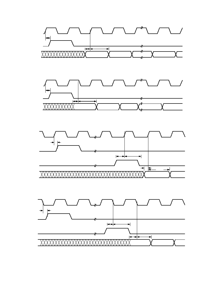
AD6623
8
t
DSFO0A
t
SSDI0
t
HSDI0
SCLK
SDFO
SDIN
DATAn
Figure 8. Serial Port Timing, Master Mode (SCS = 0), Channel is Self-Framing
t
DSFO1
t
HSDI1
SCLK
SDFO
SDIN
DATAn
t
SSDI1
Figure 9. Serial Port Timing, Slave Mode (SCS = 1), Channel is Self-Framing
t
DSFO0B
DATAn
SDIN
SCLK
SDFO
t
SSDI0
t
HSFI0
t
SSFI0
nCLKs
SDFI
t
HSDI0
Figure 10. Serial Port Timing, Master Mode (SCS = 0), Channel is External-Framing
t
DSFO1
t
HSDI1
DATAn
SDIN
SCLK
SDFO
t
HSFI1
t
SSFI1
nCLKs
SDFI
t
SSDI1
Figure 11. Serial Port Timing, Slave Mode (SCS = 1), Channel is External-Framing
REV. 0
AD6623
9
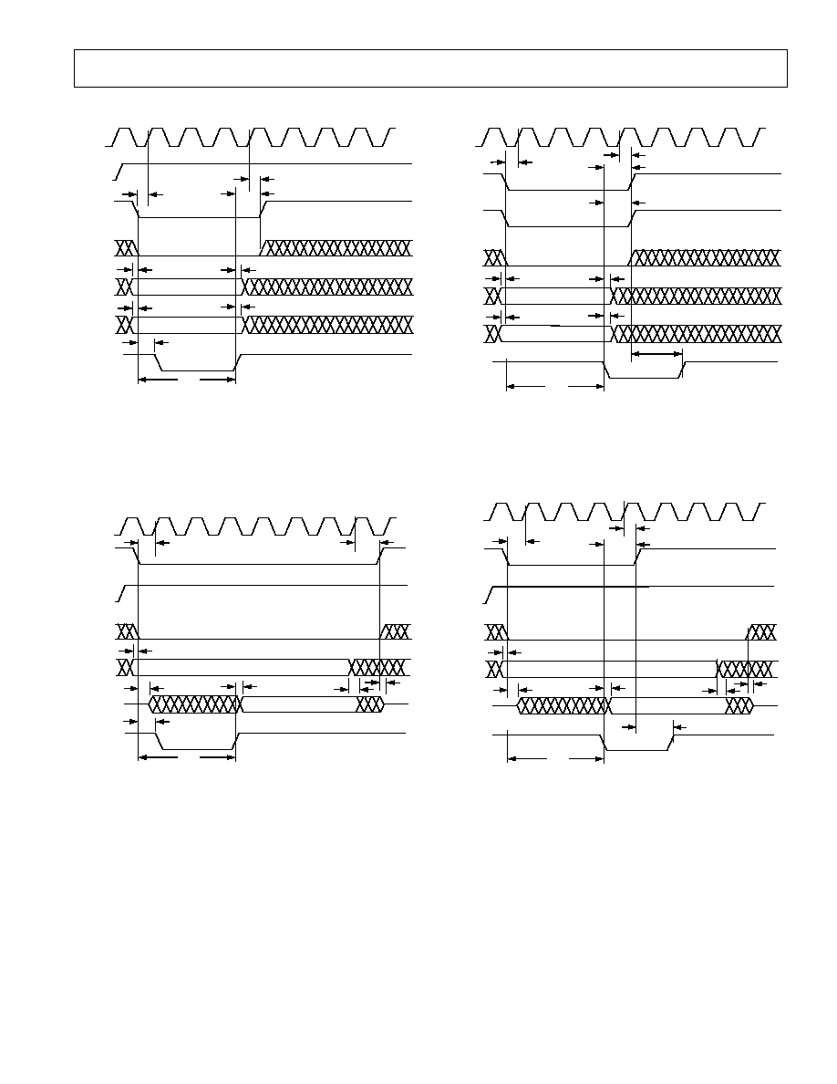
TIMING DIAGRAMS--INM MICROPORT MODE
CLK
RD (DS)
WR (RW)
CS
A[2:0]
D[7:0]
RDY
(
DTACK)
t
SC
t
HC
t
HWR
t
SAM
t
SAM
t
HAM
t
DRDY
VALID DATA
VALID ADDRESS
t
HAM
t
ACC
NOTES
1.
t
ACC
ACCESS TIME DEPENDS ON THE ADDRESS ACCESSED. ACCESS TIME IS
MEASURED FROM FE OF
WR TO THE RE OF RDY.
2.
t
ACC
REQUIRES A MAXIMUM 9 CLK PERIODS.
Figure 12. INM Microport Write Timing Requirements
CLK
RD (DS)
WR (RW)
A[2:0]
D[7:0]
RDY
(
DTACK)
t
SC
t
SAM
t
ZD
t
DRDY
VALID DATA
VALID ADDRESS
t
ACC
t
HC
CS
t
ZD
t
HAM
NOTES
1.
t
ACC
ACCESS TIME DEPENDS ON THE ADDRESS ACCESSED. ACCESS
TIME IS MEASURED FROM FE OF
WR TO THE RE OF RDY.
2.
t
ACC
REQUIRES A MAXIMUM OF 13 CLK PERIODS AND APPLIES TO
A[2:0] = 7, 6, 5, 3, 2, 1
t
DD
Figure 13. INM Microport Read Timing Requirements
TIMING DIAGRAMS--MNM MICROPORT MODE
CLK
DS (RD)
CS
A[2:0]
D[7:0]
DTACK
(RDY)
t
SC
t
HC
t
HRW
t
SAM
t
SAM
t
HAM
VALID DATA
VALID ADDRESS
t
HAM
t
ACC
NOTES
1.
t
ACC
ACCESS TIME DEPENDS ON THE ADDRESS ACCESSED. ACCESS TIME IS
MEASURED FROM FE OF
DS TO THE FE OF DTACK.
2.
t
ACC
REQUIRES A MAXIMUM 9 CLK PERIODS.
RW (
WR)
t
DDTACK
t
HDS
Figure 14. MNM Microport Write Timing Requirements
CLK
DS (RD)
RW (
WR)
A[2:0]
D[7:0]
DTACK
(RDY)
t
SC
t
SAM
t
ZD
VALID DATA
VALID ADDRESS
t
ACC
t
HC
CS
t
ZD
t
HAM
t
DD
t
DDTACK
t
HDS
NOTES
1.
t
ACC
ACCESS TIME DEPENDS ON THE ADDRESS ACCESSED. ACCESS TIME IS
MEASURED FROM FE OF
DS TO THE FE OF DTACK.
2.
t
ACC
REQUIRES A MAXIMUM 13 CLK PERIODS.
Figure 15. Motorola Microport Read Timing Requirements

REV. 0
AD6623
10
ORDERING GUIDE
Model
Temperature Range
Package Description
Package Option
AD6623AS
40
°C to +70°C (Ambient)
128-Lead MQFP (Metric Quad Flatpack)
S-128A
AD6623ABC
40
°C to +85°C (Ambient)
196-Lead BGA (Ball Grid Array)
BC-196
AD6623S/PCB
MQFP Evaluation Board with AD6623 and Software
AD6623BC/PCB
BGA Evaluation Board with AD6623 and Software
ABSOLUTE MAXIMUM RATINGS
*
Supply Voltage . . . . . . . . . . . . . . . . . . . . . . . . . . . . . . . . . 3.6 V
Input Voltage . . . . . . . . . . . . . . 0.3 V to +5 V (5 V Tolerant)
Output Voltage Swing . . . . . . . . . . 0.3 V to VDDIO + 0.3 V
Load Capacitance . . . . . . . . . . . . . . . . . . . . . . . . . . . . 200 pF
Junction Temperature Under Bias . . . . . . . . . . . . . . . . . 125
°C
Storage Temperature Range . . . . . . . . . . . . 65
°C to +150°C
Lead Temperature (5 sec) . . . . . . . . . . . . . . . . . . . . . . . 280
°C
*Stresses greater than those listed above may cause permanent damage to the
device. These are stress ratings only; functional operation of the devices at these
or any other conditions greater than those indicated in the operational sections of
this specification is not implied. Exposure to absolute maximum rating conditions
for extended periods may affect device reliability.
THERMAL CHARACTERISTICS
128-Lead MQFP:
JA
= 33
°C/W, no airflow
JA
= 27
°C/W, 200 lfpm airflow
JA
= 24
°C/W, 400 lfpm airflow
196-Lead BGA:
JA
= 26.3
°C/W, no airflow
JA
= 22
°C/W, 200 lfpm airflow
Thermal measurements made in the horizontal position on a
2-layer board.
EXPLANATION OF TEST LEVELS
I.
100% Production Tested
II.
100% Production Tested at 25
°C, and Sample Tested at
Specified Temperatures
III. Sample Tested Only
IV. Parameter Guaranteed by Design and Analysis
V.
Parameter is Typical Value Only
WARNING!
ESD SENSITIVE DEVICE
CAUTION
ESD (electrostatic discharge) sensitive device. Electrostatic charges as high as 4000 V readily
accumulate on the human body and test equipment and can discharge without detection. Although
the AD6623 features proprietary ESD protection circuitry, permanent damage may occur on
devices subjected to high-energy electrostatic discharges. Therefore, proper ESD precautions are
recommended to avoid performance degradation or loss of functionality.
REV. 0
AD6623
11
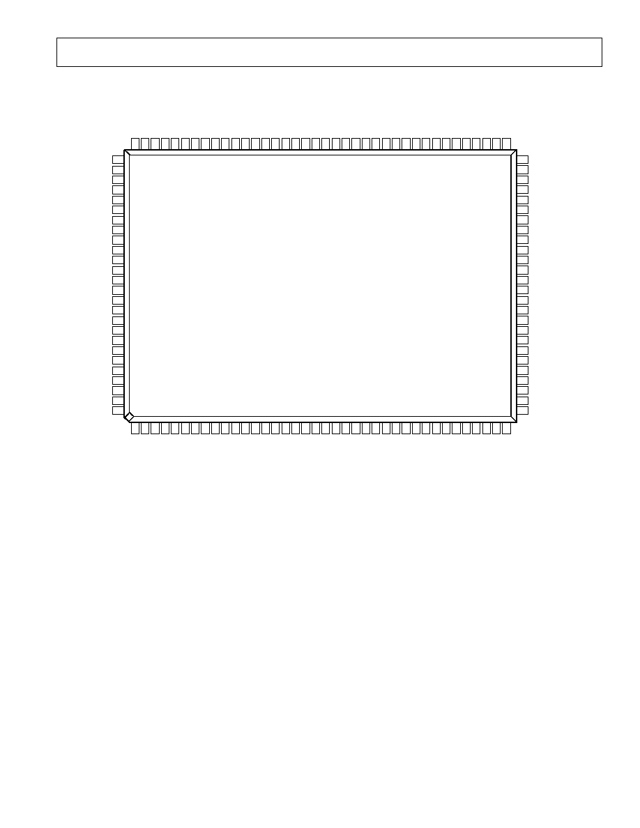
PIN CONFIGURATION
128-Lead MQFP
92
93
95
90
91
88
89
87
96
86
94
81
82
83
84
79
80
78
76
77
85
75
73
74
71
72
69
70
67
68
66
65
98
99
101
97
10
2
10
0
41
42
43
44
46
47
48
49
39
45
40
62
61
60
64
63
59
55
50
51
52
53
54
56
57
58
11
10
16
15
14
13
18
17
20
19
22
21
12
24
23
26
25
28
27
30
29
32
31
5
4
3
2
7
6
9
8
1
34
33
36
35
38
37
120
121
122
123
124
125
126
127
128
119
111
118
117
116
115
114
113
112
110
109
108
107
106
105
104
103
TOP VIEW
(Not to Scale)
SDFIC
GND
SDFIB
SDFOB
SCLKB
SDINA
SDFOA
SCLKA
TDI
TDO
TMS
SDFIA
VDD
GND
D4
D3
D2
D1
VDDIO
VDD
D0
DS(RD)
DTACK(RDY)
RW(
WR)
GND
GND
GND
MODE
A2
A1
A0
GND
TCK
TRST
GND
GND
INOUT0
GND
GND
INOUT1
INOUT2
INOUT3
INOUT4
VDDIO
INOUT11
INOUT12
VDDIO
INOUT13
INOUT14
INOUT15
INOUT16
SYNC3
GND
OEN
GND
GND
GND
OUT0
OUT1
GND
OUT3
OUT4
OUT5
OUT6
VDDIO
OUT7
OUT8
OUT9
OUT10
GND
GND
GND
OUT11
OUT12
OUT13
OUT14
VDDIO
OUT15
OUT16
OUT17
QOUT
GND
GND
GND
GND
GND
GND
D6
D7
OUT2
VDD
CS
RESET
SYNC0
SYNC1
GND
GND
GND
INOUT17
INOUT5
INOUT6
INOUT7
INOUT8
GND
GND
GND
INOUT9
INOUT10
AD6623
QIN
SYNC2
GND
CLK
VDD
GND
D5
GND
VDDIO
SDFID
SDIND
SDFOD
SCLKD
VDDIO
SDINC
SDFOC
SDINB
SCLKC
VDD
GND

REV. 0
AD6623
12
128 PIN FUNCTION DESCRIPTIONS
Pin Number
Mnemonic
Type
Description
1, 35, 9, 1921, 31, 32, 3436, 38, 39,
42, 5254, 6465, 68, 72, 8385, 95, 96,
98, 99, 102, 103, 116, 128
GND
P
Ground Connection
2
OEN
1
I
Active High Output Enable Pin
29, 28, 27, 25, 24, 23, 22, 18, 17, 16, 15,
13, 12, 11, 10, 8, 7, 6
OUT[17:0]
O/T
Parallel Output Data
47, 59, 66, 104, 127
VDD
P
2.5 V Supply
14, 26, 41, 78, 90, 110, 122
VDDIO
P
3.3 V Supply
30
QOUT
O/T
When HIGH indicates Q Output Data
(Complex Output Mode)
33, 37, 40, 43, 44, 45, 46, 48
D[7:0]
I/O/T
Bidirectional Microport Data
49
DS (RD)
I
INM Mode: Read Signal, MNM Mode: Data Strobe Signal
50
DTACK
(RDY)
O
Acknowledgment of a Completed Transaction (Signals when
µP Port Is Ready for an Access) Open Drain, Must Be
Pulled Up Externally
51
RW (
WR)
I
Active HIGH Read, Active Low Write
55
MODE
I
Sets Microport Mode: MODE = 1, MNM Mode; MODE = 0,
INM Mode
56, 57, 58
A[2:0]
I
Microport Address Bus
60
CS
I
Chip Select, Active low enable for
µP Access
61
RESET
2
I
Active Low Reset Pin
62
SYNC0
1
I
SYNC Signal for Synchronizing Multiple AD6623s
63
SYNC1
1
I
SYNC Signal for Synchronizing Multiple AD6623s
67
CLK
1
I
Input Clock
69
SYNC2
1
I
SYNC Signal for Synchronizing Multiple AD6623s
70
QIN
1
I
When HIGH indicates Q input data (Complex Input Mode)
71, 7477, 7982, 8689, 9194, 97
INOUT[17:0]
1
I/O
Wideband Input/Output Data (Allows Cascade of Multiple
AD6623 Chips In a System)
73
SYNC3
1
I
SYNC Signal for Synchronizing Multiple AD6623s
100
TRST
2
I
Test Reset Pin
101
TCK
1
I
Test Clock Input
105
SDFIA
I
Serial Data Frame Input--Channel A
106
TMS
2
I
Test Mode Select
107
TDO
O
Test Data Output
108
TDI
1
I
Test Data Input
109
SCLKA
I/O
Bidirectional Serial Clock--Channel A
111
SDFOA
O
Serial Data Frame Sync Output--Channel A
112
SDINA
1
I
Serial Data Input--Channel A
113
SCLKB
I/O
Bidirectional Serial Clock--Channel B
114
SDFOB
O
Serial Data Frame Sync Output--Channel B
115
SDFIB
I
Serial Data Frame Input --Channel B
117
SDFIC
I
Serial Data Frame Input--Channel C
118
SDINB
1
I
Serial Data Input--Channel B
119
SCLKC
I/O
Bidirectional Serial Clock--Channel C
120
SDFOC
O
Serial Data Frame Sync Output--Channel C
121
SDINC
1
I
Serial Data Input--Channel C
123
SCLKD
I/O
Bidirectional Serial Clock--Channel D
124
SDFOD
O
Serial Data Frame Sync Outpu--Channel D
125
SDIND
1
I
Serial Data Input--Channel D
126
SDFID
I
Serial Data Frame Input--Channel D
NOTES
1
Pins with a Pull-Down resistor of nominal 70 k
.
2
Pins with a Pull-Up resistor of nominal 70 k
.
REV. 0
AD6623
13
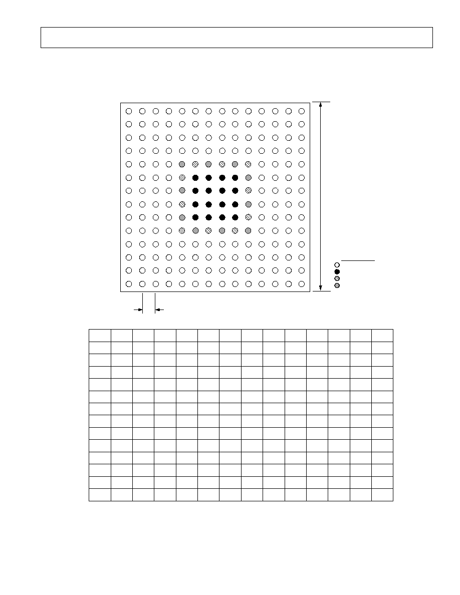
PIN CONFIGURATION
196-Lead BGA
A
B
C
D
E
F
G
H
J
K
L
M
N
P
NC = NO CONNECT
1
NC
OUT2
OUT5
OUT8
OUT9
OUT11
OUT14
OUT16
QOUT
NC
2
OUT1
OUT4
OUT4
OUT10
OUT13
D6
3
OUT0
OUT3
OUT6
OUT12
OUT17
OUT15
D7
4
SDFID
OEN
SDFOD
D4
D5
D2
5
SDINC
SDIND
VDDIO
VDD
VDDIO
VDD
VDDIO
VDD
D1
D3
6
SDINB
SDFOC
SKLKD
VDD
GND
GND
GND
GND
VDDIO
DTACK
(RDY)
D0
7
SDFOB
SDFIC
SKLKC
VDDIO
GND
GND
GND
GND
VDD
MODE
(ALE)
RW(
WR)
8
SCLKB
SDINA
SDFIB
VDD
GND
GND
GND
GND
VDDIO
A1
9
SCLKA
TDI
SDFOA
VDDIO
GND
GND
GND
GND
VDD
RESET
A0
A2
10
TDO
TMS
VDD
VDDIO
VDD
VDDIO
VDD
VDDIO
SYNC0
CS
11
SDFIA
TRST
SYNC1
12
TCK
IN2
IN3
IN6
IN12
IN16
QIN
13
IN5
IN8
IN11
IN14
IN17
CLK
14
NC
IN0
IN1
IN4
IN7
IN9
IN10
IN13
IN15
SYNC3
SYNC2
NC
BALL LEGEND
I/O
GROUND
CORE POWER
RING POWER
15mm sq.
1.0mm
A
B
C
D
E
F
G
H
J
K
L
M
N
P
1
2
3
4
5
6
7
8
9
10
11
12
13
14
TOP VIEW
DS(RD)

REV. 0
AD6623
14
196-PIN FUNCTION DESCRIPTIONS
Mnemonic
Type
Function
POWER SUPPLY
VDD
P
2.5 V Supply
VDDIO
P
3.3 V IO Supply
GND
G
Ground
INPUTS
INOUT[17:0]
1
I/O
A Input Data (Mantissa)
QIN
1
I
When HIGH Indicates Q Input Data (Complex Input Mode)
RESET
2
I
Active LOW Reset Pin
CLK
1
I
Input Clock
SYNC0
1
I
All Sync Pins Go to All Four Output Channels
SYNC1
1
I
All Sync Pins Go to All Four Output Channels
SYNC2
1
I
All Sync Pins Go to All Four Output Channels
SYNC3
1
I
All Sync Pins Go to All Four Output Channels
SDINA
1
I
Serial Data Input--Channel A
SDINB
1
I
Serial Data Input--Channel B
SDINC
1
I
Serial Data Input--Channel C
SDIND
1
I
Serial Data Input--Channel D
CS
I
Active LOW Chip Select
CONTROL
SCLKA
I/O
Bidirectional Serial Clock--Channel A
SCLKB
I/O
Bidirectional Serial Clock--Channel B
SCLKC
I/O
Bidirectional Serial Clock--Channel C
SCLKD
I/O
Bidirectional Serial Clock--Channel D
SDFOA
O
Serial Data Frame Sync Output--Channel A
SDFOB
O
Serial Data Frame Sync Output--Channel B
SDFOC
O
Serial Data Frame Sync Output--Channel C
SDFOD
O
Serial Data Frame Sync Output--Channel D
SDFIA
I
Serial Data Frame Input--Channel A
SDFIB
I
Serial Data Frame Input--Channel B
SDFIC
I
Serial Data Frame Input--Channel C
SDFID
I
Serial Data Frame Input--Channel D
OEN
1
I
Active High Output Enable Pin
MICROPORT CONTROL
D[7:0]
I/O/T
Bidirectional Microport Data
A[2:0]
I
Microport Address Bus
DS (RD)
I
Active Low Data Strobe (Active Low Read)
DTACK (RDY)
2
O/T
Active Low Data Acknowledge (Microport Status Bit)
RW (
WR)
I
Read Write (Active Low Write)
MODE
I
Intel or Motorola Mode Select
OUTPUTS
OUT[17:0]
O
Wideband Output Data
QOUT
O
When HIGH Indicates Q Output Data (Complex Output Mode)
JTAG AND BIST
TRST
2
I
Test Reset Pin (Active Low)
TCK
1
I
Test Clock Input
TMS
2
I
Test Mode Select Input
TDO
O/T
Test Data Output
TDI
1
I
Test Data Input
NOTES
1
Pins with a Pull-Down resistor of nominal 70 k
.
2
Pins with a Pull-Up resistors of nominal 70 k
.

REV. 0
AD6623
15
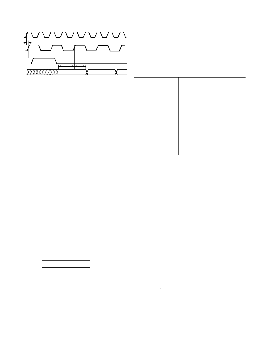
SERIAL DATA PORT
The AD6623 has four independent Serial Ports (A, B, C, and D),
and each accepts data to its own channel (A, B, C, or D) of the
device. Each Serial Port has four pins: SCLK (Serial CLocK), SDFO
(Serial Data Frame Out), SDFI (Serial Data Frame In), and SDIN
(Serial Data INput). SDFI and SDIN are inputs, SDFO is an output,
and SCLK is either input or output depending on the state of SCS
(Serial Clock Slave: 0xn16, Bit 4). Each channel can be operated
either as a Master or Slave channel depending upon SCS. The Serial
Port can be self-framing or accept external framing from the SFDI
pin or from the previous adjacent channel (0xn16, Bits 7 and 6).
Serial Master Mode (SCS = 0)
In master mode, SCLK is created by a programmable internal
counter that divides CLK. When the channel is "sleeping," SCLK
is held low. SCLK becomes active on the first rising edge of CLK
after Channel sleep is removed (D0 through D3 of external
address 4). Once active, the SCLK frequency is determined by
the CLK frequency and the SCLK divider, according to the
equations below.
AD6623 mode:
f
f
SCLKdivider
SCLK
CLK
=
+ 1
(1)
AD6622 mode:
f
f
SCLKdivider
SCLK
CLK
=
×
+
2
1
(
)
(2)
The SCLK divider is a 5-bit unsigned value located at Internal
Channel Address 0xn0D (Bits 40), where "n" is 1, 2, 3, or 4 for
the chosen channel A, B, C, or D, respectively. The user must
select the SCLK divider to insure that SCLK is fast enough to
accept full input sample words at the input sample rate. See the
design example at the end of this section. The maximum SCLK
frequency is equal to the CLK when operating in AD6623 mode
serial clock master. When operating in AD6622 compatible mode,
the maximum SCLK frequency is one-half the CLK. The minimum
SCLK frequency is 1/32 of the CLK frequency in AD6623 mode
or 1/64 of the CLK frequency when in AD6622 mode. SDFO
changes on the positive edge of SCLK when in master mode. SDIN
is captured on positive edge when SCLK is in master mode.
Serial Slave Mode (SCS = 1)
Any of the AD6623 serial ports may be operated in the serial slave
mode. In this mode, the selected AD6623 channel requires that
an external device such as a DSP to supply the SCLK. This is
done to synchronize the serial port to meet an external timing
requirement. SDIN is captured on negative edge of SCLK when
in slave mode.
Self-Framing Mode
In this mode Bit 7 of register 0xn16 is set low. The serial data
frame output, SDFO, generates a self-framing data request and
is pulsed high for one SCLK cycle at the input sample rate. In
this mode, the SDFI pin is not used, and the SDFO signal would
be programmed to be a serial data frame request (0xn16, Bit 5 = 0).
SDFO is used to provide a sync signal to the host. The input
sample rate is determined by the CLK divided by channel interpo-
lation factor. If the SCLK rate is not an integer multiple of the
input sample rate, then the SDFO will continually adjust the
period by one SCLK cycle to keep the average SDFO rate equal
to the input sample rate. When the channel is in sleep mode, SDFO
is held low. The first SDFO is delayed by the channel reset latency
after the Channel Reset is removed. The channel reset latency
varies dependent on channel configuration.
External Framing Mode
In this mode Bit 7 of register 0xn16 is set high. The external
framing can come from either the SDFI pin (0xn16, Bit 6 = 0)
or the previous adjacent channel (0xn16, Bit 6 = 1). In the case
of external framing from a previous channel, it uses the internal
frame end signal for serial data frame syncing. When in master
mode, SDFO and SDFI transition on the positive edge of SCLK,
and SDIN is captured on the positive edge of SCLK. When in
slave mode, SDFO and SDFI transition on the negative edge of
SCLK, and SDIN is captured on the negative edge of SCLK.
Serial Port Cascade Configuration
In this case the SDFO signal from the last channel of the first
chip would be programmed to be a serial data frame end (SFE:
0xn16, Bit 5 = 1). This SDFO signal would then be fed as an
input for the second cascaded chip's SDFI pin input. The second
chip would be programmed to accept external framing from the
SDFI pin (0xn16, Bit 7 = 1, Bit 6 = 0).
Serial Data Format
The format of data applied to the serial port is determined by
the RCF mode selected in Control Register 0xn0C. Below is a
table showing the RCF modes and input data format that it sets.
Table I. Serial Data Format
0xn0C
0xn0C
0xn0C
Serial Data
RCF
Bit 6
Bit 5
Bit 4
Word Length
Mode
0
0
0
32
FIR
0
0
1
/4-DQPSK
0
1
0
GMSK
0
1
1
MSK
1
0
0
24 (Bit 9 is high)
16 (Bit 9 is low)
FIR,
compact
1
0
1
8-PSK
1
1
0
3 /8-8-PSK
1
1
1
QPSK
The serial data input, SDIN, accepts 32-bit words as channel input
data. The 32-bit word is interpreted as two 16-bit two's comple-
ment quadrature words, I followed by Q, MSB first. This results in
linear I and Q data being provided to the RCF. The first bit is
shifted into the serial port starting on the next rising edge of SCLK
after the SDFO pulse. Figure 16 shows a timing diagram for SCLK
master (SCS = 0) and SDFO set for frame request (SFE = 0).
REV. 0
AD6623
16
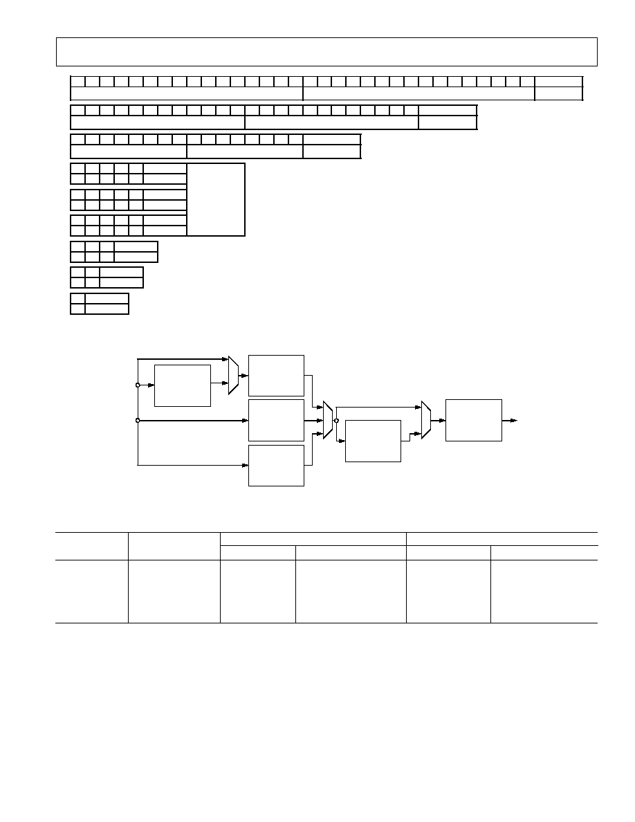
PROGRAMMABLE RAM COEFFICIENT FILTER (RCF)
Each channel has a fully independent RAM Coefficient Filter (RCF).
The RCF accepts data from the Serial Port, processes it, and passes
the resultant I and Q data to the CIC filter. A variety of processing
options may be selected individually or in combination, including
PSK and MSK modulation, FIR filtering, all-pass phase equalization,
and scaling with arbitrary ramping. See Table III.
Table III. Data Format Processing Options
Processing Block
Input Data
Output Data
Interpolating FIR Filter
I and Q
I and Q
PSK Modulator
2 or 3 bits
per symbol
Unfiltered I
and Q:
/4-QPSK,
8-PSK, or
3 /8-8-PSK
MSK Modulator
1 bit per symbol
Filtered MSK
or GSM I and Q
QPSK
2 bits per symbol
Filtered QPSK
I and Q
All-pass Phase Equalizer
I and Q
I and Q
Scale and Ramp
I and Q
I and Q
OVERVIEW OF THE RCF BLOCKS
The Serial Port passes data to the RCF with the appropriate
format and bit precision for each RCF configuration, see Figure 17.
The data may be modulated vectors or unmodulated bits. I and
Q vectors are sent directly to the Interpolating Fir Filter. Unmodu-
lated bits may be sent to the PSK Modulator, the Interpolating
MSK Modulator, or the Interpolating QPSK Modulator. The PSK
Modulator produces unfiltered I and Q vectors at the symbol
rate which are then passed through the Interpolating FIR Filter.
The Interpolating MSK Modulator and the Interpolating QPSK
Modulator produce oversampled, pulse-shaped vectors directly
without employing the Interpolating FIR Filter. When possible,
the MSK and QPSK modulators are recommended for increased
throughput and decreased power consumption compared to
Interpolating FIR Filter. In addition, the Interpolating MSK
Modulator can realize filters with nonlinear inter-symbol inter-
ference, achieving excellent accuracy for GMSK applications.
After interpolation, an optional Allpass Phase Equalizer (APE)
can be inserted into the signal path. The APE can realize any real,
stable, two-pole, two-zero all-pass filter at the RCF's interpolated
rate. This is especially useful to precompensate for nonlinear
phase responses of receive filters in terminals, as specified by IS-95.
When active, the APE utilizes shared hardware with the interpo-
lating modulators and filter, which may reduce the allowed RCF
throughput, inter-symbol interference, or both. See Figure 18.
t
DSDFO0A
t
HSDI0
SCLK
SDFO
SDI
DATAn
CLK
t
SSDI0
CLKn
t
SSDI0
Figure 16. Serial Port Switching Characteristics
As an example of the Serial Port operation, consider a CLK fre-
quency of 62.208 MHz and a channel interpolation of 2560. In
that case, the input sample rate is 24.3 kSPS (62.208 MHz/2560),
which is also the SDFO rate. Substituting, f
SCLK
32 f
SDFO
into the equation and solving for SCLKdivider, we find the mini-
mum value for SCLKdivider according to the equation below.
SCLKdivider
f
f
CLK
SFDO
×
32
(3)
Evaluating this equation for our example, SCLKdivider must be
less than or equal to 79. Since the SCLKdivider channel register
is a 5-bit unsigned number it can only range from 0 to 31.
Any value in that range will be valid for this example, but if it is
important that the SDFO period is constant, then there is another
restriction. For regular frames, the ratio f
SCLK
/f
SDFO
must be equal
to an integer of 32 or larger. For this example, constant SDFO
periods can only be achieved with an SCLK divider of 31 or less.
See Table II for usable SCLK divider values and the corresponding
SCLK and f
SCLK
/f
SDFO
ratio for the example of L = 2560.
In conclusion, SDFO rate is determined by the AD6623 CLK
rate and the interpolation rate of the channel. The SDFO rate is
equal to the channel input rate. The channel interpolation is
equal to RCF interpolation times CIC5 interpolation, times
CIC2 interpolation:
L
L
L
L
M
RCF
CIC
CRIC
CRIC
=
×
×
5
2
2
(4)
The SCLK divide ratio is determined by SCLKdivider as shown
in the previous equation. The SCLK must be fast enough to
input 32 bits of data prior to the next SDFO. Extra SCLKs are
ignored by the serial port.
Table II. Example of Usable SCLK Divider
Values and f
SCLK
/f
SDPO
Ratios for L = 2560
SCLKdivisor
f
SCLK
/f
SDFO
0
2560
1
1280
3
640
4
512
7
320
9
256
15
160
19
128
31
80
REV. 0
AD6623
17
31
30
29
28
27
26
25
24
23
22
21
20
19
18
17
16
15
14
13
12
11
10
9
8
7
6
5
4
3
2
1
0
BIT
< msb, I, lsb >
< msb, Q, lsb >
FIR
23
22
21
20
19
18
17
16
15
14
13
12
11
10
9
8
7
6
5
4
3
2
1
0
BIT
< msb, I, lsb >
< msb, Q, lsb >
COMPACT FIR
15
14
13
12
11
10
9
8
7
6
5
4
3
2
1
0
BIT
< msb, I, lsb >
< msb, Q, lsb >
COMPACT FIR
4
3
2
1
0
BIT
m
s
D1
D2
D0
8PSK
4
3
2
1
0
BIT
SERIAL SYNC
m
s
X
D1
D0
QPSK
RAMP
4
3
2
1
0
BIT
M
S
X
X
D0
MSK/GSM
2
1
0
BIT
0
D1
D0
8PSK
1
0
BIT
D1
D0
QPSK
0
BIT
D0
MSK/GSM
Figure 17. Data Formats Supported by the AD6623 when
SCLK Master (SCS = 0), and SFDO Set for Frame Request (SFE = 0)
INTERPOLATING
FIR
FILTER
INTERPOLATING
MSK
MODULATOR
INTERPOLATING
QPSK
MODULATOR
ALLPASS
PHASE
EQUALIZER
PSK
MODULATOR
SCALE
AND
RAMP
DATA FROM SERIAL PORT
DATA TO CIC FILTERS
Figure 18. RCF Block Diagram
Table IV. FIR Filter Internal Precision
Minimum
Maximum
Signal
x y Notation
Decimal
Hexadecimal (h)
Decimal
Hexadecimal (h)
I and Q Inputs
1.15
1.00000
+1.00000
0.999969
0.FFFE
Coefficients
1.15
1.00000
+1.00000
0.999969
0.FFFE
Product
2.18
0.99969
+3.00020
1.000000
1.00000
Sum
4.18
7.00000
+8.0000
7.999996
7.FFFFC
FIR Output
1.17
1.00000
+1.00000
0.999992
0.FFFF8
The Scale and Ramp block adjusts the final magnitude of the
modulated RCF output. A synchronization pulse from the SYNC03
pins or serial words can be used to command this block to ramp
down, pause, and ramp up to a new scale factor. The shape of
the ramp is stored in RAM, allowing complete sample by sample
control at the RCF interpolated rate. This is particularly useful
for time division multiplexed standards such as GSM/EDGE.
Modulator configurations can be updated while the ramp is quiet,
allowing for GSM and EDGE timeslots to be multiplexed together
without resetting or reconfiguring the channel. Each of the RCF
processing blocks is discussed in greater detail in the following
sections.
INTERPOLATING FIR FILTER
The Interpolating FIR Filter realizes a real, sum-of-products filter
on I and Q inputs using a single interleaved Multiply-Accumulator
(MAC) running at the CLK rate. The input signal is interpolated
by integer factors to produce arbitrary impulse responses up to
256 output samples long.
Each bus in the data path carries bipolar two's complement values.
For the purpose of discussion, we will arbitrarily consider the radix
point positioned so that the input data ranges from 1 to just
below 1. In Figure 19, the data buses are marked x y to denote
finite precision limitations. A bus marked x y has x bits above
the radix and y bits below the radix, which implies a range from
REV. 0
AD6623
18
2
x1
to 2
x1
2
y
in 2
y
steps. The range limits are tabulated in
Table IV for each bus. The hexadecimal values are bit-exact and
each MSB has negative weight. Note that the Product bus range is
limited by result of the multiplication and the two most significant
bits are the same except in one case.
DMEM
32 16
CMEM
256 16
INPUT
ACCUMULATOR
PRODUCT
4.18
1.15
INPUT
1.15
COEF
1.15
2.18
1.17
OUTPUT
2
0
, 2
1
, 2
2
, OR 2
3
Figure 19. Interpolating FIR Filter Block Diagram
The RCF realizes a FIR filter with optional interpolation. The FIR
filter can produce impulse responses up to 256 output samples
long. The FIR response may be interpolated up to a factor of 256,
although the best filter performance is usually achieved when the
RCF interpolation factor (L
RCF
) is confined to eight or below. The
256 16 coefficient memory (CMEM) can be divided among an
arbitrary number of filters, one of which is selected by the Coef-
ficient Offset Pointer (channel address 0x0B). The polyphase
implementation is an efficient equivalent to an integer up-sampler
followed FIR filter running at the interpolated rate.
The AD6623 RCF realizes a sum-of-products filter using a polyphase
implementation. This mode is equivalent to an interpolator followed
by a FIR filter running at the interpolated rate. In the functional
diagram below, the interpolating block increases the rate by the RCF
interpolation factor (L
RCF
) by inserting L
RCF
1 zero valued samples
between every input sample. The next block is a filter with a finite
impulse response length (N
RCF
) and an impulse response of h[n],
where n is an integer from 0 to N
RCF
1.
The difference equation for Figure 20 is written below, where h[n]
is the RCF impulse response, b[n] is the interpolated input sample
sequence at point `b' in the diagram above, and c[n] is the output
sample sequence at point `c' in Figure 20.
N
RCF
TAP
FIR FILTER
h[n]
L
RCF
f
IN
L
RCF
b
a
c
f
IN
f
IN
L
RCF
Figure 20. RCF Interpolation
c n
h n
b n
k
N
RCF
[ ]
=
[ ]
×
[ ]
=
k
0
1
(5)
This difference equation can be described by the transfer function
from point `b' to `c' as:
H
z
h n
z
bc
k
N
RCF
( )
=
[ ]
×
=
0
1
1
(6)
The actual implementation of this filter uses a polyphase decom-
position to skip the multiply-accumulates when b[nk] is zero.
Compared to the diagram above, this implementation has the benefits
of reducing by a factor of L
RCF
both the time needed to calculate
an output and the required data memory (DMEM). The price of
these benefits is that the user must place the coefficients into the coefficient
memory (CMEM) indexed by the interpolation phase. The process of
selecting the coefficients and placing them into the CMEM is broken
into three steps shown below.
The FIR accepts two's complement I and Q samples from the serial
port with a fixed-point resolution of 16 bits each. When the serial port
provides data with less precision, the LSBs are padded with zeroes.
The Data-Mem stores the most recent 16 I and Q pairs for a total
of 32 words. The size of the Data-Mem limits the RCF impulse
response to 16 L
RCF
output samples. When the data words from
the Serial Port have fewer than 16 bits, the LSBs are padded with
zeroes. The Data-Mem can be accessed through the Microport
from 0x20 to 0x5F above the processing channel's base internal
address, while the channel's Prog bit is set (external address 4).
In order to avoid start-up transients, the Data-Mem should be
cleared before operation. The Prog bit must then be reset to
enable normal operation.
The Coef-Mem stores up to 256 16-bit filter coefficients. The Coef-
Mem can be accessed through the Microport from 0x800 to 0x8FF
above the processing channel's base internal address, while the channel's
Prog bit is set (external address 4). For AD6622 compatibility, the lower
128 words are also mirrored from 0x080 to 0x0FF above the processing
channel's base internal address, while the Prog bit is set. To avoid
start-up transients, the Data-Mem should be cleared before operation.
The Prog bit must then be reset to enable channel operation.
There is a single Multiply-Accumulator (MAC) on which both the
I and Q operations must be interleaved. Two CLK cycles are required
for the MAC to multiply each coefficient by an I and Q pair. The
MAC is also used for four additional CLK cycles if the All-pass
Phase Equalizer is active.
The size of the Data-Mem and Coef-Mem combined with the
speed of the MAC determine the total number of the taps per
phase (T
RCF
) that may be calculated. T
RCF
is the number of
RCF input samples that influence each RCF output sample.
The maximum available T
RCF
is calculated by the equation below.
T
least of
floor
L
floor
f
f
APE
RCF
RCF
CLK
SDO
×
×
16
256
2
2
,
,
(7)
The impulse response length at the output of the RCF is determined
by the product of the number of interfering input samples (T
RCF
)
and the RCF interpolation factor (L
RCF
), as shown by equation
(8) below. The values of N
RCF
and T
RCF
are programmed into control
registers. L
RCF
is not a control register, but N
RCF
and T
RCF
must
be set so that L
RCF
is an integer. If the integer interpolation by
the RCF results in an inconvenient sample rate at the output of
the RCF, the desired output rate can usually be achieved by
selecting non-integer interpolation in the resampling CIC
2
filter.
N
T
L
RCF
RCF
RCF
=
×
(8)
REV. 0
AD6623
19
Table V. RCF Control Registers
Channel
Bit
Address
Width
Description
0x0A
16
158: N
RCF
1 B; 70: N
RCF
1 A
0x0B
8
70: O
RCF
0x0C
10
9: Ch. A Compact FIR Input Word Length
0: 16 bits8 I followed by 8 Q
1: 24 bits12 I followed by 12 Q
8: Ch. A RCF PRBS Enable
7: Ch A RCF PRBS Length
0: 15
1: 8,388,607
64: Ch. A RCF Mode Select
000 = FIR
001 = p/4-DQPSK Modulator
010 = GMSK Look-Up Table
011 = MSK Look-Up Table
100 = FIR compact mode
101 = 8-PSK
110 = 3p/8-8PSK Modulator
111 = QPSK Look-Up Table
30: Ch. A RCF Taps per Phase
0x0D
8
76: RCF Coarse Scale (g):
00 = 0 dB
01 = 6 dB
10 = 12 dB
11 = 18 dB
5: Ch. A Allpass Ph. Eq. Enable
40: Serial Clock Divider (1, ..., 32)
0x0E
16
152: Ch. A Unsigned Scale Factor
10: Reserved
0x0F
18
1716: Ch. A Time Slot Sync Select
00: Sync0 (See 0x001 Time Slot)
01: Sync1
10: Sync2
11: Sync3
150: Ch. A RCF Scale Hold-Off Counter
1) Ramp Down (if Ramp is enabled)
2) Update Scale and Mode
3) Ramp Up (if Ramp is enabled)
0x110
16
150: Ch. A RCF Phase EQ Coef1
0x111
16
150: Ch. A RCF Phase EQ Coef2
0x112
16
150: Ch. A RCF MPSK Magnitude 0
0x113
16
150: Ch. A RCF MPSK Magnitude 1
0x114
16
150: Ch. A RCF MPSK Magnitude 2
0x115
16
150: Ch. A RCF MPSK Magnitude 3
0x116
8
7: Reserved
6: Ch. A Serial Data Frame Select
0: Serial Data Frame Request
1: Serial Data Frame End
Channel
Bit
Address
Width Description
5: Ch. A External SDFI Select
0: Internal SDFI
1: External SDFI
4: Ch. A SCLK Slave Select
0: Master
1: Slave
3: Ch. A Serial Fine Scale Enable
2: Ch. A Serial Time Slot Sync Enable
(ignored in FIR mode)
1: Ch. A Ramp Interpolation Enable
0: Ch. A Ramp Enable
0x117
6
50: Ch. A Mode 0 Ramp Length, R01
0x118
6
50: Ch. A Mode 1 Ramp Length, R11
0x119
5
40: Ch. A Ramp Rest Time, Q
0x11A0x11F
Reserved
0x1200x13F 16
150: Ch. A Data Memory
0x1400x17F 16
1514: Reserved
130: Ch. A Power Ramp Memory
0x1800x1FF 16
150: Ch. A Coefficient Memory
This address is mirrored at 0x9000x97F
and contiguously extended at
0x9800x9FF
PSK MODULATOR
The PSK Modulator is an AD6623 extension feature that is
only available when the control register bit 0x000:7 is high.
The PSK Modulator creates 32-bit complex inputs to the
Interpolating FIR Filter from two or three data bits captured
by the serial port. The FIR Filter operates exactly as if the 32-
bit word came directly from the serial port. There are three
PSK modulation options to choose from: /4-DQPSK, 8-PSK,
and 3 /8-8-PSK. Every symbol of any of these modulations
can be represented by one of the 16 phases shown in Figure 21.
0
Figure 21. 16-Phase Modulations
REV. 0
AD6623
20
All of these phase locations are represented in rectangular coor-
dinates by only four unique magnitudes in the positive and negative
directions. These four values are read from four channel registers
that are programmed according to the following table, which
gives the generic formulas and a specific example. The example
is notable because it is only 0.046 dB below full-scale and the
16-bit quantization is so benign at that magnitude, that the rms
error is better than 122 dBc. It is also worth noting that because
none of the phases are aligned with the axes, magnitudes slightly
beyond 0.16 dB above full-scale are achievable.
Table VI. Program Registers
Channel
Register
Magnitude M
Magnitude E 0x7F53
0x12
M 3 cos(p/16)
0x7CE1
0x13
M 3 cos(3p/16)
0x69DE
0x14
M 3 cos(5p/16)
0x46BD
0x15
M 3 cos(7p/16)
0x18D7
Using the four channel registers from the preceding table, the PSK
Modulator assembles the 16 phases according to Table VII.
Table VII. PSK Modulator Phase
Phase
I Value
Q Value
0
0x12
0x15
1
0x13
0x14
2
0x14
0x13
3
0x15
0x12
4
0x15
0x12
5
0x14
0x13
6
0x13
0x14
7
0x12
0x15
8
0x12
0x15
9
0x13
0x14
10
0x14
0x13
11
0x15
0x12
12
0x15
0x12
13
0x14
0x13
14
0x13
0x14
15
0x12
0x15
The following three sections show how the phase values are
created for each PSK modulation mode.
/4-DQPSK Modulation
IS-136 compliant /4-DQPSK modulation is selected by setting
the channel register 0x0C: 64 to 001b. The phase word is calculated
according to the following diagram. The two LSBs of the serial
input word update the payload bits once per symbol. The QPSK
Mapper creates a data dependent static phase word (Sph) which
is added to a time dependent rotating phase word (Rph). The Rph
starts at zero when the RCF is reset or switches modes via a sync
pulse. Otherwise, the Rph increments by two on every symbol.
SERIAL
QPSK
MAPPER
SPH
[1:0]
[3:0]
PHASE
[3:0]
[3:0]
RPH
2
Figure 22. QPSK Mapper
The Sph word is calculated by the QPSK Mapper according to
the following truth table.
Table VIII. QPSK Mapper Truth Table
Serial [1:0]
Sph [3:0]
00b
0
01b
4
11b
8
10b
12
8-PSK Modulation
IS-136+ compliant 8-PSK modulation is selected by setting the
channel register 0x0C: 64 to 101b. The Phase word is calculated
according to the following diagram. The three LSBs of the serial
input word update the payload bits once per symbol.
SERIAL
8PSK
MAPPER
[2:0]
PHASE
[3:0]
Figure 23. 8-PSK Mapper
The Phase word is calculated by the 8-PSK Mapper according
to the following truth table:
Table IX. 8-PSK Mapper Truth Table
Serial [2:0]
Sph [3:0]
111b
0
011b
2
010b
4
000b
6
001b
8
101b
10
100b
12
110b
14
3 /8-8-PSK Modulation
EDGE compliant 3 /8-8-PSK modulation is selected by setting the
channel register 0x0C: 64 to 110b. The phase word is calculated
according to the following diagram. The three LSBs of the serial
input word update the payload bits once per symbol. The 8-PSK
Mapper creates a data-dependent static phase word (Sph) which is
added to a time-dependent rotating phase word (Rph). The 8-PSK
Mapper operates exactly as described in the preceding 8-PSK
Modulation section. The Rph starts at zero when the RCF is reset
or switches modes via a sync pulse. Otherwise, the Rph increments
by three on every symbol.
REV. 0
AD6623
21
(2
15
) 2, or 0.00006103515625. The register values, in hexadecimal,
and the corresponding coefficient weight from positive full-scale
through zero to negative full-scale is illustrated in Table X.
Table X. Coefficient Weights
Register Value
Coefficient Weight
0x7FFF
1.999938964844
..
0x0001
0.00006103515625
0x0000
0
0xFFFF
0.00006103515625
..
0x8001
1.999938964844
0x8000
2
Table XI shows the recommended b
1
and b
2
coefficients for the
respective oversampling rate.
Table XI. b
1
and b
2
Coefficients
Oversampling
b
0
b
1
b
2
4
1
1.45514
0.57832
5
1
1.56195
0.64526
6
1
1.63412
0.69414
8
1
1.72513
0.76047
SCALE AND RAMP
Scale factors can be range from 0 to [CHF]1/[CHF] with a
resolution 1/[CHF]
FINE SCALING
AD6623 allows fine scaling of the RCF output signal. A scale
factor of 12 to 14 bits is available through the Microport. The
Microport fine scale factor is located in Channel Register 0xn0E.
RCF POWER RAMPING
The output of the RCF will be multiplied by a 14-bit ramping
profile before entering the CIC filters. It is a RAM program-
mable engine that starts indexing through ramping coefficients
when the RAMP bit works its way through the chain. It will then
count a programmable number of samples and then RAMP down
in reverse order. This will allow the ramping values to update at
a modest rate relative to the DAC and still contain the spectral
leakage associated with the ramping. A user should provide
through the MicroPort the ramping coefficient values, the number
of samples to ramp up, and one bit to define the air-interface
standard. The programmable power ramp up/down unit allows
power ramping on time-slot basis as specified from some wireless
transmission technologies (e.g, TDMA).
CASCADED INTEGRATOR COMB (CIC)
INTERPOLATING FILTERS
The I and Q outputs of the RCF stage are interpolated by two
cascaded integrator comb (CIC) filters. The CIC section is sepa-
rated into three discrete blocks: a fifth order filter (CIC5), a second
order resampling filter (rCIC2), and a scaling block (CIC Scaling).
The CIC5 and rCIC2 blocks each exhibit a gain that changes with
respect to their rate change factors, L
rCIC2
, M
rCIC2
and L
CIC5
. The
product of these gains must be compensated for in a shared CIC
Scaling block and can be done to within 6 dB The remaining
compensation can come from the RCF (in the form of coeffi-
cient scaling) or the fine scaling unit.
SERIAL
8PSK
MAPPER
SPH
[2:0]
[3:0]
PHASE
[3:0]
[3:0]
RPH
3
Figure 24. 3
/8-8-PSK Mapper
MSK Look-Up Table
The MSK Look-Up Table mode for the RCF is selected in Control
Register 0x10C. In the MSK Mode, the RCF performs arbitrary
pulse-shaping based on four symbols of impulse response. For the
MSK Mode (3, [16] bits), the serial input format is 11 bits of scaling
(MSB first) followed by 1 bit of data. The 11 bits can be used to
scale the input data.
GMSK Look-Up Table
The GMSK Look-Up Table mode for the RCF is selected in Control
Register 0x10C. In the GMSK Mode, the RCF performs arbitrary
pulse-shaping based on four symbols of impulse response. For the
GMSK Mode (3, [16] bits), the serial input format is 11 bits of
scaling (MSB first) followed by 1 bit of data. The 11 bits can be used
to scale the input data.
QPSK Look-Up Table
The QPSK Filter mode for the RCF is selected in Control
Register 0xX0C. In the QPSK Mode, the RCF performs baseband
linear pulse-shaping based on filter impulse response up to 12
symbols. For the QPSK Mode (3, [16]bits), the serial input format
is 13 bits of scaling (MSB first) followed by one bit I and then
one bit Q. The 13 bits can be used to scale the input data.
PHASE EQUALIZER
The IS-95 Standard includes a phase equalizer after matched
filtering at the baseband transmit side of a base station. This
filter pre-distorts the transmitted signal at the base station in
order to compensate for the distortion introduced to the received
signal by the analog baseband filtering in a handset. The AD6623
includes this functionality in the form of an Infinite Impulse
Response (IIR) all-pass filter in the RCF. This Phase Equalizer
pre-distort filter has the following transfer function:
H z
Y z
X z
b z
b z
z
b z
b
( )
( )
( )
=
= +
+
+
+
1
1
2
1
2
2
2
(9)
Z
1
Z
1
Z
1
Z
1
X(z)
Y(z)
b
2
b
1
Figure 25. Second Order All-Pass IIR Filter
The Phase Equalizer is enabled/disabled in Control Register
0xn0D Bit 5. The coefficients b
1
and b
2
are located in Control
Registers 0xn10 and 0xn11 respectively
The format for b
1
and b
2
is two's complement fractional binary
with a range of (2, 2). With one bit for sign at most significant bit
position there are 15 bits for magnitude. The value of one bit is
REV. 0
AD6623
22
CIC Scaling
The scale factor S
CIC
is a programmable unsigned integer
between 4 and 32. This is a combined scaler for the CIC5 and
rCIC2 stages. The overall gain of the CIC section is given by
the equation below
CIC Gain
L
L
CIC
rCIC
S
CIC
_
=
×
×
5
4
2
2
(10)
CIC5
The first CIC filter stage, the CIC5, is a fifth order interpolating
cascaded integrator comb whose impulse response is completely
defined by its interpolation factor, L
CIC5
. The value L
CIC5
1 can
be independently programmed for each channel at location 0xn09.
2S
CIC
M
rCIC2
L
rCIC2
L
CIC5
CIC_SCALE
rCIC2
CIC5
Figure 26. CIC5
While this control register is 8 bits wide, L
CIC5
should be confined
to the range from 1 to 32 to avoid the possibility of internal
overflow for full scale inputs. The output rate of this stage is given
by the equation below.
f
f
L
CIC
CIC
CIC
2
5
5
=
×
(11)
The transfer function of the CIC5 is given by the following
equations with respect to the CIC5 output sample rate, f
samp5
.
CIC
z
z
z
L
CIC
5
1
1
5
1
5
( )
=
(12)
The SCIC value can be independently programmed for each
channel at Control Register 0xn06. S
CIC
may be safely calculated
according to equation (13) below to ensure the net gain through
the CIC stages.
SCIC serves to frame which bits of the CIC output are transferred
to the NCO stage. This results in controlling the data out of the
CIC stages in 6 dB Increments. For the best dynamic range, S
CIC
should be set to the smallest value possible (lowest attenuation)
without creating an overflow condition. This can be safely
accomplished using the equation below. To ensure the CIC
output data is in range, equation (13) must always be met. The
maximum total interpolation rate may be limited by the amount
of scaling available.
S
ceil
L
L
CIC
CIC
CIC
×
(
)
+
(
)
(
)
4
2
5
2
2
log
log
(13)
0
58
S
CIC
(14)
This polynomial fraction can be completely reduced as follows
demonstrating a finite impulse response with perfect phase
linearity for all values of L
CIC5
.
CIC
z
z
z
e
k
k
L
j
k
L
k
L
CIC
CIC
CIC
5
0
1
5
1
2
1
1
5
5
5
5
( )
=
=
=
=
(15)
The frequency response of the CIC5 can be expressed as follows.
The initial 1/L
CIC5
factor normalizes for the increased rate,
which is appropriate when the samples are destined for a DAC
with a zero order hold output. The maximum gain is L
CIC5
4
at
baseband, but internal registers peak in response to various
dynamic inputs. As long as L
CIC5
is confined to 32 or less, there
is no possibility of overflow at any register.
CIC
f
L
L
f
f
f
f
CIC
CIC
CIC
CIC
5
1
5
5
5
5
5
( )
=
×
sin
sin
(16)
The pass band droop of CIC5 should be calculated using this equation
and can be compensated for in the RCF stage. The gain should
be calculated from the CIC scaling section above.
As an example, consider an input from the RCF whose bandwidth
is 0.141 of the RCF output rate, centered at baseband. Interpolation
by a factor of five reveals five images, as shown below.
10
dB
10
30
3
3
2
1
0
1
2
50
70
90
110
130
150
Figure 27. Interpolation Images
The CIC5 rejects each of the undesired images while passing the
image at baseband. The images of a pure tone at channel center
(DC) are nulled perfectly, but as the bandwidth increases the
rejection is diminished. The lower band edge of the first image
always has the least rejection. In this example, the CIC5 is inter-
polating by a factor of five and the input signal has a bandwidth
of 0.141 of the RCF output sample rate. The plot below shows
110 dBc rejection of the lower band edge of the first image. All
other image frequencies have better rejection.
10
dB
10
30
3
3
2
1
0
1
2
50
70
90
110
130
150
Figure 28. 110 dBc Rejection
REV. 0
AD6623
23
Table XII lists maximum bandwidth that will be rejected to various
levels for CIC5
interpolation factors from 1 to 32. The example
above corresponds to the listing in the 110 dB column and the
L
CIC5
= 5 row. It is worth noting here that the rejection of the
CIC5 improves as the interpolation factor increases.
Table XII. Max Bandwidth of Rejection for L
CIS
Values
110 dB
100 dB
90 dB
80 dB
70 dB
Full
Full
Full
Full
Full
0.101
0.127
0.160
0.203
0.256
0.126
0.159
0.198
0.246
0.307
0.136
0.170
0.211
0.262
0.325
0.136
0.175
0.217
0.269
0.333
0.143
0.178
0.220
0.272
0.337
0.144
0.179
0.222
0.275
0.340
0.145
0.180
0.224
0.276
0.341
0.146
0.181
0.224
0.277
0.342
0.146
0.182
0.225
0.278
0.343
0.147
0.182
0.226
0.278
0.344
0.147
0.182
0.226
0.279
0.344
0.147
0.183
0.226
0.279
0.345
0.147
0.183
0.226
0.279
0.345
0.148
0.183
0.227
0.280
0.345
0.148
0.183
0.227
0.280
0.345
0.148
0.183
0.227
0.280
0.346
0.148
0.183
0.227
0.280
0.346
0.148
0.183
0.227
0.280
0.346
0.148
0.184
0.227
0.280
0.346
0.148
0.184
0.227
0.280
0.346
0.148
0.184
0.227
0.280
0.346
0.148
0.184
0.227
0.280
0.346
0.148
0.184
0.227
0.280
0.346
0.148
0.184
0.227
0.281
0.346
0.148
0.184
0.227
0.281
0.346
0.148
0.184
0.227
0.281
0.346
0.148
0.184
0.227
0.281
0.346
0.148
0.184
0.227
0.281
0.346
0.148
0.184
0.227
0.281
0.346
0.148
0.184
0.227
0.281
0.346
0.148
0.184
0.228
0.281
0.346
rCIC2
The rCIC2 filter is a second order Cascaded Resampling Integrator
Comb filter whose impulse response is completely defined by
its rate change factors, L
rCIC2
and M
rCIC2
. The resampler is
implemented using a unique technique that does not require
a high-speed clock (but it's still completely jitter-free), thus
simplifying the design and saving power. The resampler allows for
noninteger relationships between the input data rate and the master
clock. This allows easier implementation of systems that are either
multimode or require a master clock that is not a multiple of the
input data rate to be used.
The value of L
rCIC2
is limited from 1 to 4096 subject to some restric-
tions based upon the chosen LCIC5 value as shown in Table XIII.
Table XIII. Maximum Permissible L
RC1C2
Values
Chosen L
CIC5
Value
Maximum Allowed L
rCIC2
32
4096
31
1162
2430
L
rCIC
L
CIC
2
30
4
2
2
3
= [
]
log (
)
23
3836
122
4096
Two parameters determine the rate change in this block. They are
the interpolation factor (L
rCIC2
, 12 bits) and the decimation factor
(M, 9 bits). When combined, and subject to the maximum values
of L
rCIC2
, the total rate change can be any fraction in the form of:
R
L
M
L
M
rCIC2
1 1
4096 1
512
=
,
,
(17)
The only constraint is that the ratio L/M must be greater than or
equal to one. This implies that the rCIC2 has a net interpolation
of 1 or more.
Resampling is implemented by apparently increasing the input
sample rate by the factor L, using zero stuffing for the new data
samples. Following the resampler is a second order cascaded
integrator comb filter. Filter characteristics are determined only
by the fractional rate change (L/M).
The filter can produce output signals at the full CLK rate of the
AD6623. The output rate of this stage is given by the equation
below.
f
L
M
f
out
rCIC
rCIC
rCIC
=
2
2
2
(18)
Both L
rCIC2
and M
rCIC2
are unsigned integers. The interpolation
rate (L
rCIC2
) may be from 1 to 4096 and the decimation (M
rCIC2
)
may be between 1 and 512. The stage can be bypassed by setting
the L and M to 1.
The transfer function of the rCIC2 is given by the following
equations with respect to the rCIC2 output sample rate, f
out
.
rCIC
z
z
z
L
rCIC
2
1
1
2
1
2
( )
=
(19)
The frequency response of the rCIC2 can be expressed as follows.
The maximum gain is L
rCIC2
at baseband. The initial M
rCIC2
/L
rCIC2
factor normalizes for the increased rate, which is appropriate when
the samples are destined for a DAC with a zero order hold output.
rCIC
f
M
L
L
f
f
f
f
rCIC
rCIC
rCIC
out
out
2
2
2
2
2
( )
=
×
sin
sin
(20)
The pass-band droop of CIC5 should be calculated using this
equation and can be compensated for in the RCF stage. The
gain should be calculated from the CIC scaling section above.
The values M
rCIC2
1, L
rCIC2
1 can be independently programmed
for each channel at locations 0xn07, 0xn08. While these control
registers are nine bits and 12 bits wide respectively, M
rCIC2
1 and
REV. 0
AD6623
24
L
rCIC2
1 should be confined to the ranges shown by Table XIII
according to the interpolation factor of the CIC5. Exceeding the
recommended guidelines may result in overflow for input sequences
at or near full scale. While relatively large ratios of L
rCIC2
/M
rCIC2
allow for the larger overall interpolations with minimal power
consumption, L
rCIC2
/M
rCIC2
should be minimized to achieve the
best overall image rejection.
As an example, consider an input from the CIC5 whose bandwidth
is 0.0033 of the CIC5 rate, centered at baseband. Interpolation
by a factor of five reveals five images, as shown below.
150
2
1
dB
0
1
2
130
110
90
70
50
30
10
10
Figure 29. CIC5 Interpolation Images
The rCIC2 rejects each of the undesired images while passing
the image at baseband. The images of a pure tone at channel
center (DC) are nulled perfectly, but as the bandwidth increases
the rejection is diminished. The lower band edge of the first
image always has the least rejection. In this example, the rCIC2
is interpolating by a factor of five and the input signal has a
bandwidth of 0.0033 of the CIC5 output sample rate. Figure 30
below shows 110 dBc rejection of the lower band edge of the
first image. All other image frequencies have better rejection.
10
dB
10
30
3
3
2
1
0
1
2
50
70
90
110
130
150
Figure 30. rCIC2 110 dBc
Table XIV lists maximum bandwidth that will be rejected to
various levels for CIC2
interpolation factors from 1 to 32. The
example above corresponds to the listing in the 110 dB column
and the L
CIC2
= 5 row. The rejection of the CIC2 improves as
the interpolation factor increases.
Table XIV. Maximum Bandwidth of Rejection for L
CIC2
Values
110 dB
100 dB
90 dB
80 dB
70 dB
Full
Full
Full
Full
Full
0.0023
0.0040
0.0072
0.0127
0.0226
0.0029
0.0052
0.0093
0.0165
0.0292
0.0032
0.0057
0.0101
0.0179
0.0316
0.0033
0.0059
0.0105
0.0186
0.0328
0.0034
0.0060
0.0107
0.0189
0.0334
0.0034
0.0061
0.0108
0.0192
0.0338
0.0035
0.0062
0.0109
0.0193
0.0341
0.0035
0.0062
0.0110
0.0194
0.0343
0.0035
0.0062
0.0110
0.0195
0.0344
0.0035
0.0062
0.0110
0.0195
0.0345
0.0035
0.0062
0.0111
0.0196
0.0346
0.0035
0.0062
0.0111
0.0196
0.0346
0.0035
0.0063
0.0111
0.0196
0.0347
0.0035
0.0063
0.0111
0.0197
0.0347
0.0035
0.0063
0.0111
0.0197
0.0347
0.0035
0.0063
0.0111
0.0197
0.0348
0.0035
0.0063
0.0111
0.0197
0.0348
0.0035
0.0063
0.0111
0.0197
0.0348
0.0035
0.0063
0.0111
0.0197
0.0348
0.0035
0.0063
0.0111
0.0197
0.0348
0.0035
0.0063
0.0111
0.0197
0.0348
0.0035
0.0063
0.0111
0.0197
0.0348
0.0035
0.0063
0.0112
0.0197
0.0348
0.0035
0.0063
0.0112
0.0198
0.0349
0.0035
0.0063
0.0112
0.0198
0.0349
0.0035
0.0063
0.0112
0.0198
0.0349
0.0035
0.0063
0.0112
0.0198
0.0349
0.0035
0.0063
0.0112
0.0198
0.0349
0.0035
0.0063
0.0112
0.0198
0.0349
0.0035
0.0063
0.0112
0.0198
0.0349
0.0035
0.0063
0.0112
0.0198
0.0349
NUMERICALLY CONTROLLED OSCILLATOR/TUNER (NCO)
Each channel has a fully independent tuner. The tuner accepts
data from the CIC filter, tunes it to a digital Intermediate Fre-
quency (IF), and passes the result to a shared summation block.
The tuner consists of a 32-bit quadrature NCO and a Quadrature
Amplitude Mixer (QAM). The NCO serves as a local oscillator and
the QAM translates the interpolated channel data from baseband
to the NCO frequency. The worst case spurious signal from the
NCO is better than 100 dBc for all output frequencies. The
tuner can produce real or complex outputs as requested by the
shared summation block.
In the complex mode, the NCO serves as a quadrature local oscillator
running at f
CLK
/2 capable of producing any frequency step between
f
CLK
/4 and +f
CLK
/4 with a resolution of f
CLK
/2
33
(0.0121 Hz for
f
CLK
= 104 MHz).
In the real mode, the NCO serves as a quadrature local oscillator
running at f
CLK
capable of producing any frequency step between
f
CLK
/2 and +f
CLK
/2 with a resolution of f
CLK
/2
32
(0.0242 Hz for
f
CLK
= 104 MHz). The quadrature portion of the output is
discarded. Negative frequencies are distinguished from positive
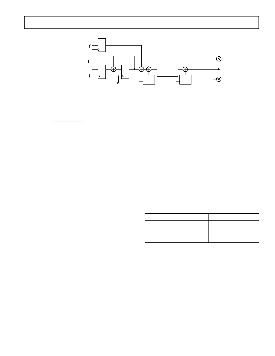
REV. 0
AD6623
25
frequencies solely by spectral inversion. The digital IF is calcu-
lated using the equation:
f
f
NCO
frequency
IF
NCO
=
×
_
2
32
(21)
where:
NCO_frequency is the value written to 0xn02,
f
IF
is the desired intermediate frequency, and
f
NCO
is f
CLK
/2 for complex outputs and f
CLK
for real outputs.
Phase Dither
The AD6623 provides a phase dither option for improving the
spurious performance of the NCO. Phase dither is enabled by
writing a "1" to Bit 3 of Channel Register 0xn01. When phase
dither is enabled, spurs due to phase truncation in the NCO are
randomized. The choice of whether phase dither is used in a system
will ultimately be decided by the system goals and the choice of IF
frequency. The 18 most significant bits of the phase accumulator
are used by the angle to Cartesian conversion. If the NCO frequency
has all zeroes below the 18
th
bit, then phase dither has no effect.
If the fraction below the 18
th
bit is near a 1/2 or 1/3 of the 18
th
bit, then spurs will accumulate separated from the IF by 1/2 or
1/3 of the CLK frequency. The smaller the denominator of this
residual fraction, the larger the spurs due to phase truncation will
be. If the phase truncation spurs are unacceptably high for a given
frequency, then the phase dither can reduce these at the penalty
of a slight elevation in total error energy. If the phase truncation
spurs are small, then phase dither will not be effective in reducing
them further, but a slight elevation in total error energy will occur.
Amplitude Dither
Amplitude dither can also be used to improve spurious performance
of the NCO. Amplitude dither is enabled by writing a "1" to Bit 4
of Channel Register at 0xn01. When enabled, amplitude dither
can reduce spurs due to truncation at the input to the QAM. If
the entire frequency word is close to a fraction that has a small
denominator, the spurs due to amplitude truncation will be large
and amplitude dither will spread these spurs effectively. Amplitude
dither also will increase the total error energy by approximately
3 dB. For this reason amplitude dither should be used judiciously.
Phase Offset
The phase offset (Channel Register 0xn04) adds an offset to the
phase accumulator of the NCO. This is a 16-bit register that is
interpreted as a 16-bit unsigned integer. Phase offset ranges
from 0 to nearly 2 radians with a resolution of /32768 radians.
This register allows multiple NCOs to be synchronized to produce
sine waves with a known phase relationship.
NCO Frequency Update and Phase Offset Update Hold-Off
Counters
The update of both the NCO frequency and phase offset
can be synchronized with internal Hold-Off counters. Both of
these counters are 16-bit unsigned integers and are clocked at
the master CLK rate. These Hold-Off counters used in conjunc-
tion with the frequency or phase offset registers, allow beam
forming and frequency hopping. See the Synchronization section
of the data sheet for additional details. The NCO phase can also
be cleared on Sync (set to 0x0000) by setting Bit 2 of Channel
Register 0xn01 high.
NCO Control Scale
The output of the NCO can be scaled in four steps of 6 dB each
via Channel Register 0xn01, Bits 10. Table XV show a break-
down of the NCO Control Scale. The NCO always has loss to
accommodate the possibility that both the I and Q inputs may
reach full-scale simultaneously, resulting in a 3 dB input magnitude.
Table XV. NCO Control Scale
0xn01 Bit 1
0xn01 Bit 0
NCO Output Level
0
0
6 dB (no attenuation)
0
1
12 dB attenuation
1
0
18 dB attenuation
1
1
24 dB attenuation
SUMMATION BLOCK
The Summation Block of the AD6623 serves to combine the
outputs of each channel to create a composite multicarrier signal.
The four channels are summed together and the result is then
added with the 18-bit Wideband Input Bus (IN[17:0]). The final
summation is then driven on the 18-bit Wideband Output Bus
(OUT[17:0]) on the rising edge of the high speed clock. If the
OEN input is high then this output bus is three-stated. If the OEN
input is low then this bus will be driven by the summed data.
The OEN is active high to allow the Wideband Output Bus to
be connected to other busses without using extra logic. Most other
busses (like 374 type registers) require a low output enable, which is
opposite of the AD6623 OEN, thus eliminating extra circuitry.
The wideband parallel input IN[17:0] is defined as bidirectional,
to support dual parallel outputs. Each parallel output produces
the sum of two of the four internal TSPs and AD6623 that can
32
32
Q
D
PN
GEN.
NCO
FREQUENCY
WORD
16
PHASE
OFFSET
16
32
32
Q
D
ANGLE TO
CARTESIAN
CONVERSION
PN
GEN.
I DATA FROM
CIC5
Q DATA FROM
CIC5
I
Q
I, Q
CLK
ON
OFF
ON
OFF
32
32
MICROPROCESSOR
INTERFACE
Figure 31. Numerically Controlled Oscillator and QAM Mixer
REV. 0
AD6623
26
drive two DACs. Channels are added in pairs (A + B), (C + D)
as shown in Figure 32.
CHANNELS
A + B
OUT
[17:0]
IN/OUT
[17:0]
CHANNELS
C + D
14-BIT
DAC
14-BIT
DAC
AD6623
Figure 32. AD6623 Driving Two DACs
The Wideband Output Bus may be interpreted as a two's comple-
ment number or as an offset binary number as defined by bit 1 of the
Summation Mode Control Register at address 0x000. When this
bit is high, then the Wideband Output is in two's complement mode
and when it is low it is configured for offset binary output data.
The MSB (bit 17) of the Wideband Output Bus is typically used
as a guard bit for the purpose of clipping the wideband output
bus when bit 0 of the Summation Mode Control Register at
address 0x000 is high. If clip detection is enabled then bit 17 of
the output bus is not used as a data bit. Instead, bit 16 will become
the MSB and is connected to the MSB of the DAC. Configuring
the DAC in this manner gives the summation block a gain of 0 dB.
When clip detection is not enabled and bit 17 is used as a data
bit then the summation block will have a gain of 6.02 dB.
There are two data output modes. The first is offset binary.
This mode is used only when driving offset binary DACs. Two's
complement mode may be used in one of two circumstances. The
first is when driving a DAC that accepts two's complement data.
The second is when driving another AD6623 in cascade mode.
When clipping is enabled, the two's complement mode output bus
will clip to 0x2FFFF for output signals more positive than the
output can express and it will clip to 0x3000 for signals more nega-
tive than the output can express. In offset binary mode the output
bus will clip to 0x3FFFF for output signals more positive than
the output can express and it will clip to 0x2000 for signals more
negative than the output can express.
The Wideband Input is always interpreted as an 18-bit two's
complement number and is typically connected to the Wideband
Output Bus of another AD6623 in order to send more than four
carriers to a single DAC. The Output Bus of the preceeding
AD6623 should be configured in two's complement mode and
clip detection disabled. The 18-bit resolution insures that the noise
and spur performance of the wideband data stream does not become
the limiting factor as large numbers of carriers are summed.
There is a two-clock cycle latency from the Wideband Input Bus
to the Wideband Output Bus. This latency may be calibrated out
of the system by use of the Start Hold-Off counter. The preceding
AD6623 in a cascaded chain can be started two CLK cycles before
the following AD6623 is started and the data from each AD6623
will arrive at the DAC on the same clock cycle. In systems where the
individual signals are not correlated, this is usually not necessary.
The AD6623 is capable of outputting both real and complex data.
When in Real mode the QIN input is tied low signaling that all
inputs on the Wideband Input Bus are real and that all outputs
on the Wideband Output Bus are real. The Wideband Input Bus
will be pulled low and no data will be added to the composite
signal if this port is unused (not connected).
If complex data is desired there are two ways this can be obtained.
The first method is to simply set the QIN input of the AD6623
high and to set the Wideband Input Bus low. This allows the AD6623
to output complex data on the Wideband Output Bus. The I data
samples would be identified when QOUT is low and the Q data
samples would be identified when QOUT is high. The second
method of obtaining complex data is to provide a QIN signal that
toggles on every rising edge of the CLK. This could be obtained
by connecting the QOUT of another AD6623 to QIN as shown
in Figure 33. In a cascaded system the QIN of the first AD6623
in the chain would typically be tied high and the QOUT of the
first AD6623 would be connected to the QIN of the following
part. All AD6623s will synchronize themselves to the QIN input
so that the proper samples are always paired and the Wideband
Output bus represents valid complex data samples. Table XV
shows different parallel input and output data bus formats as a
function of QIN and QOUT.
Table XV. Valid Output Bus Data Modes
Wideband Input
Output Data Type
QIN
IN[17:0]
OUT[17:0], QOUT
Low
Real
Real
High
Zero
Complex
Pulsed
Complex
Complex
14-BIT
DAC
OUT
[16:3]
IN
[17:0]
OUT
[17:0]
Q
IN
Q
OUT
IN
[17:0]
Q
IN
AD6623
AD6623
LOGIC1
LOGIC0
Figure 33. Cascade Operation of Two AD6623s
SYNCHRONIZATION
Three types of synchronization can be achieved with the AD6623.
These are Start, Hop, and Beam. Each is described in detail below.
The synchronization is accomplished with the use of a shadow
register and a Hold-Off counter. See Figure 34 for a simplistic
schematic of the NCO shadow register and NCO Frequency
Hold-Off counter to understand basic operation. Enabling the
clock (AD6623 CLK) for the Hold-Off counter can occur with
either a Soft_Sync (via the micro port), or a Pin Sync (via the
AD6623 Sync pin, Pin 62). The functions that include shadow
registers to allow synchronization include:
1. Start
2. Hop (NCO Frequency)
3. Beam (NCO Phase Offset)
Start
Refers to the start-up of an individual channel, chip, or multiple
chips. If a channel is not used, it should be put in the Sleep
Mode to reduce power dissipation. Following a hard reset (low
pulse on the AD6623
RESET pin), all channels are placed in
the Sleep Mode.
Start With No Sync
If no synchronization is needed to start multiple channels or mul-
tiple AD6623s, the following method should be used to initialize
the device.
1. To program a channel, it must first be set to the Program Mode
(bit high) and Sleep Mode (bit high) (Ext Address 4). The
Program Mode allows programming of data memory and coeffi-
cient memory (all other registers are programmable whether in
Program Mode or not). Since no synchronization is used, all
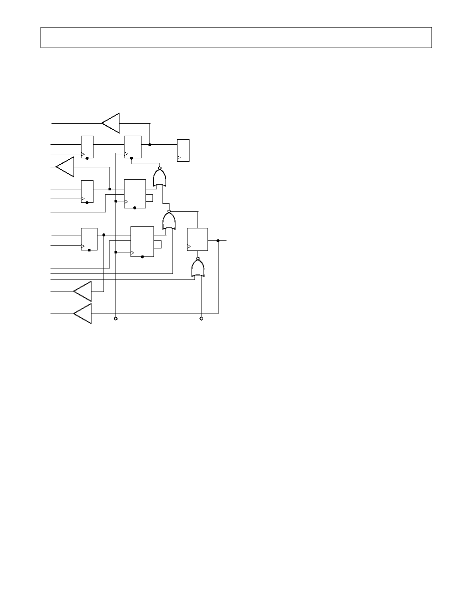
REV. 0
AD6623
27
Sync bits are set low (External Address 5). All appropriate
control and memory registers (filter) are then loaded. The
Start Update Hold-Off Counter (0xn00) should be set to 0.
2. Set the appropriate program and sleep bits low (Ext Address 4).
This enables the channel. The channel must have Program
and Sleep Mode low to activate a channel.
32
NCO SHADOW
REGISTER
Q
D
Q
D
NCO
REGISTER
NCO PHASE
ACCUMULATOR
32
32
ENA
16
Q
D
Q
D
D
PL
D
Q
CLR
SET
SLEEP
HOP
HOLDOFF
HOP
SYNC
START
HOLDOFF
HOLDOFF
COUNTER
START
COUNTER
RESET PIN
CLK
START
SYNC
16
16
16
CLR
C = 1
C = 0
ENA
C = 1
C = 0
PL
MICR
OPR
OCESSOR INTERF
A
CE
ENA
Figure 34. NCO Shadow Register and Hold-Off Counter
Start with Soft Sync
The AD6623 includes the ability to synchronize channels or chips
under microprocessor control. One action to synchronize is the
start of channels or chips. The Start Update Hold-Off Counter
(0xn00) in conjunction with the Start bit and Sync bit (Ext
Address 5) allow this synchronization. Basically the Start Update
Hold-Off Counter delays the Start of a channel(s) by its value
(number of AD6623 CLKs). The following method is used to syn-
chronize the start of multiple channels via microprocessor control.
1. Set the appropriate channels to sleep mode (a hard reset to the
AD6623 Reset pin brings all four channels up in sleep mode).
2. Write the Start Update Hold-Off Counter(s) (0xn00) to the
appropriate value (greater than 1 and less than 2
16
1). If the
chip(s) is not initialized, all other registers should be loaded
at this step.
3. Write the Start bit and the SyncX(s) bit high (Ext Address 5).
4. This starts the Start Update Hold-Off Counter counting down.
The counter is clocked with the AD6623 CLK signal. When it
reaches a count of one the sleep bit of the appropriate channel(s)
is set low to activate the channel(s).
Start with Pin Sync
A Sync pin is provided on the AD6623 to provide the most
accurate synchronization, especially between multiple AD6623s.
Synchronization of start with an external signal is accomplished
with the following method.
1. Set the appropriate channels to sleep mode (a hard reset to the
AD6623 Reset pin brings all four channels up in sleep mode).
2. Write the Start Update Hold-Off Counter(s) (0xn00) to the
appropriate value (greater than 1 and less than 2
16
1). If the
chip(s) is not initialized, all other registers should be loaded
at this step.
3. Set the Start on Pin Sync bit and the appropriate Sync Pin
Enable high (0xn01).
4. When the Sync pin is sampled high by the AD6623 CLK this
enables the count down of the Start Update Hold-Off Counter.
The counter is clocked with the AD6623 CLK signal. When it
reaches a count of one the sleep bit of the appropriate channel(s)
is set low to activate the channel(s).
Hop
A jump from one NCO frequency to a new NCO frequency. This
change in frequency can be synchronized via microprocessor
control or an external Sync signal as described below.
To set the NCO frequency without synchronization the following
method should be used.
Set Frequency No Hop
1. Set the NCO Frequency Hold-Off counter to 0.
2. Load the appropriate NCO frequency. The new frequency
will be immediately loaded to the NCO.
Hop with Soft Sync
The AD6623 includes the ability to synchronize a change in NCO
frequency of multiple channels or chips under microprocessor
control. The NCO Frequency Hold-Off counter (0xn03) in con-
junction with the Hop bit and the Sync bit (Ext Address 5) allow
this synchronization. Basically the NCO Frequency Hold-Off
counter delays the new frequency from being loaded into the NCO
by its value (number of AD6623 CLKs). The following method
is used to synchronize a hop in frequency of multiple channels
via microprocessor control.
1. Write the NCO Frequency Hold-Off (0xn03) counter to the
appropriate value (greater than 1 and less then 2
16
1).
2. Write the NCO Frequency register(s) to the new desired
frequency.
3. Write the hop bit and the Sync(s) bit high (Ext Address 5).
4. This starts the NCO Frequency Hold-Off counter counting
down. The counter is clocked with the AD6623 CLK signal.
When it reaches a count of one the new frequency is loaded
into the NCO.
Hop with Pin Sync
A Sync pin is provided on the AD6623 to provide the most
accurate synchronization, especially between multiple AD6623s.
Synchronization of hopping to a new NCO frequency with an
external signal is accomplished with the following method.
1. Write the NCO Frequency Hold-Off counter(s) (0xn03) to
the appropriate value (greater than 1 and less than 2
16
1).
2. Write the NCO Frequency register(s) to the new desired
frequency.
3. Set the Hop on Pin Sync bit and the appropriate Sync Pin
Enable high (0xn01).
4. When the Sync pin is sampled high by the AD6623 CLK
this enables the count down of the NCO Frequency Hold-Off
counter. The counter is clocked with the AD6623 CLK signal.
When it reaches a count of one the new frequency is loaded into
the NCO.

REV. 0
AD6623
28
Beam
A change in phase for a particular channel and can be synchronized
with respect to other channels or AD6623s. This change in phase
can be synchronized via microprocessor control or an external
Sync signal.
To set the amplitude without synchronization the following
method should be used.
Set Phase No Beam
1. Set the NCO Phase Offset Update Hold-Off Counter (0xn05)
to 0.
2. Load the appropriate NCO Phase Offset (0xn04). The NCO
Phase Offset will be immediately loaded.
Beam with Soft Sync
The AD6623 includes the ability to synchronize a change in NCO
phase of multiple channels or chips under microprocessor control.
The NCO Phase Offset Update Hold-Off Counter in conjunction
with the Beam bit and the Sync bit (Ext Address 5) allow this
synchronization. Basically the NCO Phase Offset Update Hold-
Off Counter delays the new phase from being loaded into the
NCO/RCF by its value (number of AD6623 CLKs). The following
method is used to synchronize a beam in phase of multiple channels
via microprocessor control.
1. Write the NCO Phase Offset Update Hold-Off Counter (0xn05)
to the appropriate value (greater than 1 and less then 2
16
1).
2. Write the NCO Phase Offset register(s) to the new desired
phase and amplitude.
3. Write the beam bit and the Sync(s) bit high (Ext Address 5).
4. This starts the NCO Phase Offset Update Hold-Off Counter
counting down. The counter is clocked with the AD6623
CLK signal. When it reaches a count of one the new phase is
loaded into the NCO.
Beam with Pin Sync
A Sync pin is provided on the AD6623 to provide the most
accurate synchronization, especially between multiple AD6623s.
Synchronization of beaming to a new NCO Phase Offset with an
external signal is accomplished using the following method.
1. Write the NCO Phase Offset Hold-Off (0xn05) counter(s) to
the appropriate value (greater than 1 and less than 2
16
1).
2. Write the NCO Phase Offset register(s) to the new desired
phase and amplitude.
3. Set the Beam on Pin Sync bit and the appropriate Sync Pin
Enable high (0xn01).
4. When the Sync pin is sampled high by the AD6623 CLK this
enables the count down of the NCO Phase Offset Hold-Off
counter. The counter is clocked with the AD6623 CLK signal.
When it reaches a count of one the new phase is loaded into
the NCO registers.
JTAG INTERFACE
The AD6623 supports a subset of IEEE Standard 1149.1 specifica-
tion. For additional details of the standard, please see IEEE Standard
Test Access Port and Boundary-Scan Architecture, IEEE-1149
publication from IEEE.
The AD6623 has five pins associated with the JTAG interface.
These pins are used to access the on-chip Test Access Port and
are listed in Table XVII.
Table XVII. Test Access Port Pins
Name
Pin Number
Description
TRST
100
Test Access Port Reset
TCK
101
Test Clock
TMS
106
Test Access Port Mode Select
TDI
108
Test Data Input
TDO
107
Test Data Output
Note that TCK and TDI are internally pulled down which is
opposite of IEEE Standard 1149.1. These pins may be connected
to external pull-up resistors, with the associated additional current
draw through the pull-ups, or left unconnected.
The AD6623 supports four op codes are shown in Table XVIII.
These instructions set the mode of the JTAG interface.
Table XVIII. Op Codes
Instruction
Op Code
IDCODE
10
BYPASS
11
SAMPLE/PRELOAD
01
EXTEST
00
The Vendor Identification Code (Table XIX) can be accessed
through the IDCODE instruction and has the following format.
Table XIX. Vendor Identification Code
MSB
Part
Manufacturer
LSB
Version Number
ID Number
Mandatory
0000
0010 0111 1000 0000
000 1110 0101
1
A BSDL file for this device is available from Analog Devices, Inc.
Contact Analog Devices for more information.
SCALING
Proper scaling of the wideband output is critical to maximize the
spurious and noise performance of the AD6623. A relatively small
overflow anywhere in the data path can cause the spurious free
dynamic range to drop precipitously. Scaling down the output
levels also reduces dynamic range relative to an approximately
constant noise floor. A well-balanced scaling plan at each point
in the signal path will be rewarded with optimum performance.
The scaling plan can be separated into two parts: multicarrier
scaling and single-carrier scaling.
Multicarrier Scaling
An arbitrary number of AD6623s can be cascaded to create a
composite digital IF with many carriers. As the number of carriers
increases, the peak to RMS ratio of the composite digital IF will
increase as well. It is possible and beneficial to limit the peak to
RMS ratio through careful frequency planning and controlled
phase offsets. Nevertheless, in most cases with a large number of
carriers, the worst-case peak is an unlikely event.
The AD6623 immediately preceding the DAC can be programmed
to clip rather than wrap around (see the Summation Block de-
scription). For a large number of carriers, a rare but finite chance of
clipping at the AD6623 wideband output will result in superior
dynamic range compared to lowering each carrier level until
clipping is impossible. This will also be the case for most DACs.
Through analysis or experimentation, an optimal output level of
individual carriers can be determined for any particular DAC.

REV. 0
AD6623
29
Single-Carrier Scaling
Once the optimal power level is determined for each carrier, one
must determine the best way to achieve that level. The maximum
SNR can be achieved by maximizing the intermediate power level
at each processing stage. This can be done by assuming the proper
level at the output and working along the following path: Sum-
mation, NCO, CIC, Ramp, RCF, and finally, Fine Scaler Unit.
The Summation Block is intended to combine multiple carriers
with each carrier at least 6 dB below full scale. For this configu-
ration, the AD6623 driving the DAC should have clip detection
enabled. OUT17 becomes a clip indicator that reports clipping
in both polarities. If the DAC requires offset binary outputs, then
the internal offset binary conversion should be enabled as well.
Any preceding cascaded AD6623s should disable clip detection
and offset binary conversion. The IN17IN0 of the first AD6623
in the cascade should be grounded. See the Summation Block
section for details. In this configuration, intermediate OUT17s will
serve as guard bits that allow intermediate sums to exceed full scale.
As long as the final output does not exceed 6 dB over full scale, the
clip detector will perform correctly.
If a single carrier needs to exceed 6 dB full scale, hardwired
scaling can be accomplished according to Table XX. This is most
useful when the AD6623 is processing a Single Wideband Carrier
such as UMTS or CDMA 2000.
Table XX. Hardwired Scaling
Max. Single
Connect to
Clip
Offset Binary
Carrier Level
DAC MSB
Detect
Compensation
12.04 dB
OUT17
N/A
Internal
6.02 dB
OUT16
±
Internal
0 dB
OUT15
+ only
0x08000
+6.02 dB
OUT14
+ only
0x0C000
The NCO/Tuner is equipped with an output scaler that ranges
from 6.02 dB to 24.08 dB below full scale, in 6.02 dB steps. See
the NCO/Tuner section for details. The best SNR will be achieved
by maximizing the input level to the NCO and using the largest
possible NCO attenuation. For example, to achieve an output
level 20 dB below full scale, one should set the CIC output level to
1.94 dB below full scale and attenuate by 18.06 dB in the NCO.
The CIC is equipped with an output scaler that ranges from 0 dB
to 186.64 dB below full scale in 6.02 dB steps. This large attenuation
is necessary to compensate for the potentially large gains associ-
ated with CIC interpolation. See the CIC section for details. For
example to achieve an output level of 1.94 dB below full scale,
with a CIC5 interpolation of 27 (114.51 dB gain) and a CIC2 inter-
polation of 3 (9.54 dB gain), one should set the CIC_Scale to 20
and the Fine Scale Unit output level to 5.59 dB below full scale.
.
.
.
.
.
1 94
9 54
114 51 20
6 02
5 59
+
×
=
(22)
The ramp unit when bypassed will have exactly 0 dB of gain and
can be ignored. When in use, the gain is dependant on what value
is stored in the last valid RMEM location. RMEM words are
14 bits [01), so when the value is positive full scale, the gain is
about 0.0005 dB; probably neglectable.
The RCF coefficients should be normalized to positive full scale.
This will yield the greatest dynamic range. The RCF is equipped
with an output scaler that ranges from 0 dB to 18.06 dB below
full scale in 6.02 dB steps. This attenuation can be used to partially
compensate for filter gain in the RCF. For example, if the maximum
gain of the RCF coefficients is 11.26 dB, the RCF coarse scale
should be set to 2 (12.04 dB). This yields an RCF output level
and fine scale input level of 0.78 dB
11 26
12 04
0 78
.
.
.
=
(23)
The fine scale unit is left to turn a 0.78 dB level into a 5.59 dB
level. This requires a gain of 4.81 dB, which corresponds to a
14-bit [02] scale value of 1264h. All subsequent rescalings
during chip operation should be relative to this maximum.
.
.
.
5 59
0 78
4 81
=
(24)
floor
h
10
2
1264
4 81
20
13
.
×
=
(25)
Finally, as described in the RCF section, there may be a worst-case
peak of a phase that is larger than the channel center gain. In the
preceding example, if the worst case to channel center ratio is larger
than 4.59 dB (potentially overflowing the RCF), then the RCF_
Coarse_Scale should be reduced by one and the CIC_Scale should
be increased by one. In the preceding example, if the worst case to
channel center ratio is larger than 5.59 dB (potentially overflowing
the RCF and CIC), then the RCF_Coarse_Scale should be reduced
by one and the NCO_Output_Scale should be increased by one.
MICROPORT INTERFACE
The MicroPort interface is the communications port between the
AD6623 and the host controller. There are two modes of bus
operation: Intel nonmultiplexed mode (INM), and Motorola non-
multiplexed mode (MNM) that is set by hard-wiring the MODE
pin to either ground or supply. The mode is selected based on the
use of the MicroPort control lines (DS or RD, DTACK or RDY,
RW or WR) and the capabilities of the host processor. See the
timing diagrams for details on the operation of both modes.
The External Memory Map provides data and address registers
to read and write the extensive control registers in the Internal
Memory Map. The control registers access global chip functions
and multiple control functions for each independent channel.
MicroPort Control
All accesses to the internal registers and memory of the AD6623
are accomplished indirectly through the use of the microprocessor
port external registers shown in Table XXI. Accesses to the Exter-
nal Registers are accomplished through the 3 bit address bus (A[2:0])
and the 8-bit data bus (D[7:0]) of the AD6623 (MicroPort).
External Address [3:0] provides access to data read from or writ-
ten to the internal memory (up to 32 bits). External Address [0]
is the least significant byte and External Address [3] is the most
significant byte. External Address [4] controls the Sleep Mode
of each channel. External Address [5] controls the sync status of
each channel. External Address [7:6] determines the Internal
Address selected and whether this address is incremented after
subsequent reads and/or writes to the internal registers.
EXTERNAL MEMORY MAP
The External Memory Map is used to gain access to the Internal
Memory Map described below. External Address [7:6] sets the
Internal Address to which subsequent reads or writes will be per-
formed. The top two bits of External Address [7] allow the user
to set the address to auto increment after reads, writes, or both.
All internal data words have widths that are less than or equal to
32 bits. Accesses to External Address [0] also triggers access to
the AD6623's internal memory map. Thus during writes to the

REV. 0
AD6623
30
internal registers, External Address [0] must be written last to
insure all data is transferred. Reads are the opposite in that
External Address [0] must be the first data register read (after setting
the appropriate internal address) to initiate an internal access.
External Address [5:4] reads and writes are transferred immediately
to internal control registers. External Address [4] is the sleep register.
The sleep bits can be set collectively by the address. The sleep bits
can be cleared by operation of start syncs (described below).
External Address [5] is the sync register. These bits are write only.
There are three types of syncs: start, hop, and beam. Each of these
can be sent to any or all of the four channels. For example, a write of
X0010100
would issue a start sync to channel C only. A write of
X1101111
would issue a beam sync and a hop sync to all channels.
The internal address bus is 12 bits wide and the internal data bus
is 32 bits wide. External address 7 is the UAR (Upper Address
Register) and stores the upper four bits of the address space in
UAR[3:0]. UAR[7:6] define the auto-increment feature. If Bit 6
is high, the internal address is incremented after an internal read.
If Bit 7 is high, the internal address is incremented after an internal
write. If both bits are high, the internal address in incremented
after either a write or a read. This feature is designed for sequential
access to internal locations. External address 6 is the LAR (Lower
Address Register) and stores the lower 8 bits of the internal
address. External addresses 3 through 0 store the 32 bits of the
internal data. All internal accesses are two clock cycles long.
Writing to an internal location with a data width of 16 bits is
achieved by first writing the upper four bits of the address to bits
3 through 0 of the UAR (bits 7 and 6 of the UAR are written to
determine whether or not the auto increment feature is enabled).
The LAR is then written with the lower eight bits of the internal
address (it doesn't matter if the LAR is written before the UAR as
long as both are written before the internal access). Since the data
width of the internal address is 16 bits, only data register 1 and data
register 0 are needed. Data register 1 must be written first because
the write to data register 0 triggers the internal access. Data register
0 must always be the last register written to initiate the internal write.
Reading from the MicroPort is accomplished in a similar manner.
The internal address is first written. A read from data register 0
activates the internal read, thus register 0 must always be read first
to initiate an internal read. This provides the 8 LSBs of the internal
read through the MicroPort (D[7:0]). Additional bytes are then
read by changing the external address (A[2:0]) and performing
additional reads. If data register 3 (or any other) is read before
data register 0, incorrect data will be read. Data register 0 must
be read first in order to transfer data from the core memory to the
external memory locations. Once the data register is read, the remaining
locations may be examined in any order.
Access to the external registers of Table XX is accomplished
in one of two modes using the
CS, DS(RD), RW(WR), and
DTACK(RDY) inputs. The access modes are Intel Nonmulti-
plexed mode and Motorola Nonmultiplexed mode. These modes
are controlled by the MODE input (MODE = 0 for INM,
MODE = 1 for MNM).
Intel Nonmultiplexed Mode (INM)
MODE must be tied low to operate the AD6623 MicroPort in
INM mode. The access type is controlled by the user with the
chip select (
CS), read (RD), and write (WR) inputs. The ready
(RDY) signal is produced by the MicroPort to communicate to
the user the MicroPort is ready for an access. RDY goes low at
the start of the access and is released when the internal cycle is
complete. See the timing diagrams for both the read and write
modes in the Specifications.
Motorola Nonmultiplexed Mode (MNM)
MODE must be tied high to operate the AD6623 MicroPort in
MNM mode. The access type is controlled by the user with the
chip select (
CS), data strobe (DS), and read/write (RW) inputs.
The data acknowledge (
DTACK) signal is produced by the
MicroPort to acknowledge the completion of an access to the user.
DTACK goes low when an internal access is complete and then
will return high after
DS is deasserted. See the timing diagrams
for both the read and write modes in the Specifications.
The
DTACK(RDY) pin is configured as an open drain so that
multiple devices may be tied together at the microprocessor/
microcontroller without contention.
The MicroPort of the AD6623 allows for multiple accesses while
CS is held low (CS can be tied permanently low if the MicroPort
is not shared with additional devices). The user can access multiple
locations by pulsing the RW(
WR) or DS(RD) lines and changing
the contents of the external three bit address bus (A[2:0]).
External Address 7 Upper Address Register (UAR)
Sets the four most significant bits of the internal address, effectively
selecting channels 1, 2, 3, or 4 (D2:D0). The autoincrement of
read and write are also set (D7:D6).
External Address 6 Lower Address Register (LAR)
Sets the internal address 8 LSBs (D7:D0).
External Address 5 Sync
This register is write only. Bits in this address control the synchro-
nization of the AD6623 channels. If the user intends to bring up
channels with no synchronization requirements then all bits of this
register should be written low. Two types of sync signals are available
with the AD6623. The first is Soft Sync. Soft Sync is software
synchronization enabled through the MicroPort. The second
synchronization method is Pin Sync. Pin Sync is enabled by a signal
Table XXI. External Registers
External Data
External Address
D7
D6
D5
D4
D3
D2
D1
D0
7:UAR
Wrinc
Rdinc
IAII
IAIO
IA9
IA8
6:LAR
IA7
IA6
IA5
IA4
IA3
IA2
IA1
IA0
5:Sync
Beam
Hop
Start
Sync D
Sync C
Sync B
Sync A
4:Sleep
Prog D
Prog C
Prog B
Prog A
Sleep D
Sleep C
Sleep B
Sleep A
3:Byte3
ID31
ID30
ID29
ID28
ID27
ID26
ID25
ID24
2:Byte2
ID23
ID22
ID21
ID20
ID19
ID18
ID17
ID16
1:Byte1
ID15
ID14
ID13
ID12
ID11
ID10
ID9
ID8
0:Byte0
ID7
ID6
ID5
ID4
ID3
ID2
ID1
ID0

REV. 0
AD6623
31
Common Function Registers (not associated with a particular channel)
Internal Address
Bit
AD6622 Compatible Description
AD6623 Extensions Description
0x000
7
AD6623 Extension = 0
1
AD6623 Extension = 1
1
65
Reserved
No Change
4
Reserved
Wideband Input Disable
3
3
Reserved
Dual Output Enable
3
2
Reserved
No Change
1
Offset Binary Outputs
1
No Change
0
Clip Wideband I/O
3
No Change
0x001
7
First Sync Only
3
No Change
6
Beam on Pin Sync
3
No Change
5
Hop on Pin Sync
3
No Change
4
Start on Pin Sync
3
No Change
3
Ch. D Sync0 Pin Enable
3
No Change
2
Ch. C Sync0 Pin Enable
3
No Change
1
Ch. B Sync0 Pin Enable
3
No Change
0
Ch. A Sync0 Pin Enable
3
No Change
0x002
230
Unused
BIST Counter
1, 3
0x003
150
Unused
BIST Value (read only)
Channel Function Registers (0x1XX = Ch. A, 0x2XX = Ch. B, 0x3XX = Ch. C, 0x4XX = Ch. D)
Internal Address
Bit
AD6622 Compatible Description
AD6623 Extensions Description
0x100
1716
Unused
Ch. A Start Sync Select
3
00: Sync0 (See 0x001)
01: Sync1
10: Sync2
11: Sync3
150
Ch. A Start HoldOff Counter
3
No Change
0x101
75
Reserved
No Change
4
Ch. A NCO Amplitude Dither Enable
No Change
3
Ch. A NCO Phase Dither Enable
No Change
2
Ch. A NCO Clear Phase Accumulator on Sync
No Change
10
Ch. A NCO Scale
No Change
00: 6 dB
No Change
01: 12 dB
No Change
10: 18 dB
No Change
11: 24 dB
No Change
0x102
310
Ch. A NCO Frequency Value
3
No Change
0x103
1716
Unused
Ch. A Hop Sync Select
3
00: Sync0 (See 0x001 Hop)
01: Sync1
10: Sync2
11: Sync3
applied to the Sync pin (Pin 62). See the Synchronization section
for detailed explanations of the different modes.
External Address 4 Sleep
Bits in this register determine how the chip is programmed and
enables the channels. The program bits (D7:D4) must be set high to
allow programming of CMEM and DMEM for each channel.
Sleep bits (D3:D0) are used to activate or sleep channels. These can
be used manually by the user to bring up a channel by simply writing
the required channel high. These bits can also be used in conjunc-
tion with the Start and Sync signals available in External Address
5 to synchronize the channels. See the Synchronization section for a
detailed explanation of different modes.
External Address 3:0 (Data Bytes)
These registers return or accept the data to be accessed for a
read or write to internal addresses
INTERNAL COUNTER REGISTERS AND ON-CHIP RAM
AD6623 and AD6622 Compatibility
The AD6623 functionality is a superset of the AD6622 functionality.
The AD6623 is pin-compatible with AD6622.
AD6622 compatibility is selected when bit 7 of Internal Control
Register 0x000 is low. In this state, all AD6623 extended control
registers are cleared. While in the AD6622 mode the unused
AD6623 pins are three-stated.
Listed below is the mapping of internal AD6623 registers. AD6622
compatibility is selected by setting 0x000:7 low. In this state, all
AD6623 extended control registers are cleared. Registers marked
as "Reserved" must be written low.

REV. 0
AD6623
32
Channel Function Registers (continued)
Internal Address
Bit
AD6622 Compatible Description
AD6623 Extensions Description
150
Ch. A NCO Frequency Update HoldOff Counter
3
No Change
0x104
150
Ch. A NCO Phase Offset
2
No Change
2
0x105
1716
Reserved
Ch. A Phase Sync Select
3
00: Sync0 (See 0x001 Beam)
01: Sync1
10: Sync2
11: Sync3
150
Ch. A NCO Phase Offset Update Holdoff Counter
3
No Change
0x106
75
Reserved
No Change
40
Ch. A CIC Scale, S
CIC
No Change
0x107
80
Reserved
Ch. A CIC2 Decimation, M
2
1
0x108
118
Reserved
Ch. A CCI2 Interpolation, L
2
1, extended
70
Ch. A C1C2 Interpolation, L
2
1
No Change
0x109
70
Ch. A C1C5 Interpolation, L
5
1
No Change
0x10A
158
Reserved
Ch. A RCF TapsB, N
RCF
1 (8 bits)
3
7
Reserved
Ch. A RCF TapsA, N
RCF
1 (new MSB)
2
60
Ch. A RCF TapsA, N
RCF
1 (7 bits)
1
No Change
2
0x10B
7
Reserved
Ch. A RCF Coef Offset, O
RCF
(new MSB)
2
60
Ch. A RCF Coefficient Offset, O
RCF
(7 bits)
1
No Change
2
0x10C
1510
Unused
Reserved
9
Unused
Ch. A Compact FIR Input Word Length
0: 16 bits--8 I followed by 8 Q
1: 24 bits--12 I followed by 12 Q
8
Unused
Ch. A RCF PRBS Enable
7
Ch. A PRBS Length
3
Ch. A RCF PRBS Length
3
0: 15
0: 15
1: 8,388,607
1: 8,388,607
6
Ch. A RCF PRBS Enable
Ch. A RCF Mode Select (1 of 3)
2
5
Ch. A RCF Mode Select (1 of 2)
3
Ch. A RCF Mode Select (2 of 3)
2
4
Ch. A RCF Mode Select (2 of 2)
3
Ch. A RCF Mode Select (3 of 3)
2
00: FIR
000: FIR
01: FIR
001: /4DQPSK
10: QPSK
010: GMSK
11: MSK
011: MSK
100: FIR, Compact Input Resolution
101: 8PSK
110: 3
/88PSK
111: QPSK
30
Ch. A RCF (Taps per Phase
3
) 1
No Change
2
0x10D
76
Ch. A RCF Coarse Scale (a)
No Change
2
00: 0 dB
01: 6 dB
10: 12 dB
11: 18 dB
5
Ch. A RCF Phase EQ Enable
No Change
40
Ch. A Serial Clock Divisor (2, 4, ...64)
Ch. A Serial Clock Divisor (1, 2,...32)
0x10E
15
Ch. A Fine Scale Factor Enable
Ch. A Unsigned Scale Factor
2
This is extended to allow values in the
range (02).
142
Ch. A RCF Unsigned Scale Factor
2
No Change
2
10
Reserved
Reserved
0x10F
1716
Unused
Ch. A Time Slot Sync Select
00: Sync0 (See 0x001 Time Slot)
01: Sync1
10: Sync2
11: Sync3
150
Ch. A RCF Scale HoldOff Counter
1
The counter is unchanged, but instead of
just scale update, when the counter hits
one, the following sequence is initiated:
1. Ramp Down (if Ramp is enabled)

REV. 0
AD6623
33
Channel Function Registers (continued)
Internal Address
Bit
AD6622 Compatible Description
AD6623 Extensions Description
2. Update RCF Mode Select registers
marked with
"2"
.
3. Ramp Up (if Ramp is enabled)
0x110
150
Ch. A RCF Phase EQ Coef1
No Change
0x111
150
Ch. A RCF Phase EQ Coef2
No Change
0x112
150
Unused
Ch. A RCF FIRPSK Magnitude 0
0x113
150
Unused
Ch. A RCF FIRPSK Magnitude 1
0x114
150
Unused
Ch. A RCF FIRPSK Magnitude 2
0x115
150
Unused
Ch. A RCF FIRPSK Magnitude 3
0x116
76
Unused
Ch. A Serial Data Frame Input Select
0x: Internal Frame Request
10: External SDFI Pad
11: Previous Channel's Frame End
5
Unused
Ch. A Serial Data Frame Output Select
0: Serial Data Frame Request
1: Serial Data Frame End
4
Unused
Ch. A Serial Clock Slave (SCS)
SCS = 0: Master Mode
(SCLK is an output)
SCS = 1: Slave Mode
(SCLK is an input)
3
Unused
Ch. A Serial Fine Scale Enable
1
2
Unused
Ch. A Serial Time Slot Sync Enable
(ignored in FIR mode)
1
Unused
Ch. A Ramp Interpolation Enable
0
Unused
Ch. A Ramp Enable
0x117
50
Unused
Ch. A Mode 0 Ramp Length, R01
0x118
40
Unused
Ch. A Mode 1 Ramp Length, R11
0x119
40
Unused
Ch. A Ramp Rest Time, Q
(No inputs requested during rest time.)
0x11A11F
Unused
No Change
0x12013F
150
Ch. A Data RAM
No Change
0x14017F
1514
Unused
No Change
130
Unused
Ch. A Ramp RAM
0x1801FF
150
Ch. A Coefficient RAM
No Change
This address is mirrored at 0x9000x97F
and contiguously extended at 0x9800x9FF
NOTES
1
Clear on
RESET.
2
These bits update after a Start or a Beam Sync. See CR 0x10F.
3
Allows dynamic updates.
(0x000) Summation Mode Control
Controls features in the summation block of the AD6623.
Bit 56:
Reserved.
Bit 4:
Low: Wideband Input Enabled.
High: Wideband Input Disabled.
Bit 3:
Low: Dual Output Disabled.
High: Dual Output Enabled.
Bit 2:
Reserved.
Bit 1:
Low: Output data will be in two's complement.
High: Output data will be in offset binary.
Bit 0:
Low: Over-range will wrap.
High: Over-range will clip to full scale.
(0x001) Sync Mode Control
Bit 7:
Ignores all but the first pin sync.
Bit 6:
Beam on pin Sync.
Bit 5:
Hop on pin Sync.
Bit 4:
High enables the count down of the Start Hold-Off
Counter. The counter is clocked with the AD6623
CLK signal. When it reaches a count of one the Sleep
bit of the appropriate channel(s) is set low to activate
the channel(s).
Bit 30:
High enables synchronization of these channels.
See the Synchronization section of the data sheet for
detailed explanation.
(0x002) BIST Counter
Sets the length, in CLK cycles, of the built-in self test.
(0x003) BIST Result
A read-only register containing the result after a self test. Must be
compared to a known good result for a given setup to determine
pass/fail.

REV. 0
AD6623
34
Channel Function Registers
The following registers are channel-specific. `0xn' denotes that
these values are represented as hexadecimal numbers; `n' repre-
sents the specified channel. Valid channels are n = 1, 2, 3, and 4.
(0xn00) Start Update Hold-Off Counter
See the Synchronization section for detailed explanation. If no
synchronization is required, this register should be set to 0.
Bit 1716: The Start Sync Select bits are used to set which
sync pin will initiate a start sequence.
Bit 150:
The Start Update Hold-Off Counter is used to synchro-
nize startup of AD6623 channels and can be used to
synchronize multiple chips. The Start Update Hold-Off
Counter is clocked by the AD6623 CLK (master clock).
(0xn01) NCO Control
Bit 1:0
Set the NCO scaling per Table XXI.
Table XXI. NCO Control (0xn01)
Bit 1
Bit 0
NCO Output Level
0
0
6 dB (no attenuation)
0
1
12 dB attenuation
1
0
18 dB attenuation
1
1
24 dB attenuation
Bit 2:
High clears the NCO phase accumulator to 0 on
either a Soft Sync or Pin Sync (see Synchronization
for details).
Bit 3:
High enables NCO phase dither.
Bit 4:
High enables NCO amplitude dither.
Bit 75:
Reserved and should be written low.
(0xn02) NCO Frequency
This register is a 32-bit unsigned integer that sets the NCO
Frequency. The NCO Frequency contains a shadow register for
synchronization purposes. The shadow can be read back directly,
the NCO Frequency cannot.
NCO
f
CLK
FREQUENCY
CHANNEL
=
×
2
32
(26)
(0xn03) NCO Frequency Update Hold-Off Counter
See the Synchronization section for detailed explanation. If no
synchronization is required, this register should be set to 0.
Bit 1716: The Hop Sync Select bits are used to set which sync
pin will initiate a hop sequence.
Bit 150:
The Hold-Off Counter is used to synchronize the
change of NCO frequencies.
(0xn04) NCO Phase Offset
This register is a 16-bit unsigned integer that is added to the phase
accumulator of the NCO. This allows phase synchronization of
multiple channels of the AD6623(s). The NCO Phase Offset contains
a shadow register for synchronization purposes. The shadow can
be read back directly, the NCO Phase Offset cannot. See the
Synchronization section for details.
(0xn05) NCO Phase Offset Update Hold-Off Counter
See the Synchronization section for a detailed explanation. If no
synchronization is required, this register should be set to 0.
Bit 1716: The Phase Sync Select bits are used to set which sync
pin will initiate a phase sync sequence.
Bit 150:
The Hold-Off Counter is used to synchronize the
change of NCO phases.
(0xn06) CIC Scale
Bits 40: Sets the CIC scaling per the equation below.
CIC
Scale
ceil
L
L
CIC
CIC
_
=
×
×
(
)
(
)
log
2
5
4
2
(27)
See the CIC section for details.
(0xn07) CIC2 Decimation 1 (M
CIC2
1)
This register is used to set the decimation in the CIC2 filter. The
value written to this register is the decimation minus one. The
CIC2 decimation can range from 1 to 512 depending upon the
interpolation of the CIC2. There is no timing error associated
with this decimation. See the CIC2 section for further details.
(0xn08) CIC2 Interpolation 1 (L
CIC2
1)
This register is used to set the interpolation in the CIC2 filter.
The value written to this register is the interpolation minus one.
The CIC2 interpolation can range from 1 to 4096. L
rCIC2
must
be chosen equal to or larger than M
rCIC2
and both must be cho-
sen such that a suitable CIC2 Scalar can be chosen. For more
details the CIC2 section should be consulted.
(0xn09) CIC5 Interpolation 1
This register sets the interpolation rate for the CIC5 filter stage
(unsigned integer). The programmed value is the CIC5 Interpo-
lation 1. Maximum interpolation is limited by the CIC scaling
available (See the CIC section).
(0xn0A) Number of RCF Coefficients 1
This register sets the number of RCF Coefficients and is limited
to a maximum of 256. The programmed value is the number of
RCF Coefficients 1. There is an A register and a B register at
this memory location. Value A is used when the RCF is operating
in mode 0 and value B is used when in mode 1. The RCF mode
bit of interest here is bit 6 of address 0xn0C.
(0xn0B) RCF Coefficient Offset
This register sets the offset for RCF Coefficients and is normally
set to 0. It can be viewed as a pointer which selects the portion
of the CMEM used when computing the RCF filter. This allows
multiple filters to be stored in the Coefficient memory space, selecting
the appropriate filter by setting the offset.
(0xn0C) Channel Mode Control 1
Bit 9:
High, selecting compact FIR mode results in 24-bit
serial word length (12 I followed by 12 Q). When
low, selecting compact FIR mode results in 16-bit
serial word length (8 I followed by 8 Q).
Bit 8:
High enables RCF Pseudo-Random Input Select.
Bit 7:
High selects a Pseudo-Random sequence length of
8,388,607. Low selects a Pseudo-Random Sequence
length of 15.
Bits 64:
Sets the channel input format as shown in Table XXII.
Table XXII. Channel Inputs
Bit 6
Bit 5
Bit 4
Input Mode
0
0
0
FIR
0
0
1
/4-DQPSK
0
1
0
GSM
0
1
1
MSK
1
0
0
Compact FIR
1
0
1
8PSK
1
1
0
3 /8-8PSK
1
1
1
QPSK

REV. 0
AD6623
35
Bit 6
Can be set through the serial port (see section on
serial word formats).
Bits 30:
Sets (N
RCF
/L
RCF
) 1
(0xn0D) Channel Mode Control 2
Bits 76:
Sets the RCF Coarse Scale as shown in Table XXIII.
Table XXIII. RCF Coarse Scale
Bit 7
Bit 6
RCF Coarse Scale (dB)
0
0
0
0
1
6
1
0
12
1
1
18
Bit 5:
High enables the RCF phase equalizer.
Bits 40:
Sets the serial clock divider (SDIV) that determines the
serial clock frequency based on the following equation.
f
CLK
SDIV
SCLK
=
+ 1
(28)
(0xn0E) Fine Scale Factor
Bits 152:
Sets the RCF Fine Scale Factor as an unsigned number
representing the values (0,2). This register is shad-
owed for synchronization purposes. The shadow can
be read back directly, the Fine Scale Factor can not.
Bits 10:
Reserved.
(0xn0F) RCF Time Slot Hold-Off Counter
Bits 1716: The Time Slot Sync Select bits are used to set which
sync pin will initiate a time slot sync sequence.
Bits 150: The Hold-Off Counter is used to synchronize the
change of RCF Fine Scale. See the Synchronization
section for a detailed explanation. If no synchroniza-
tion is required, this register should be set to 0.
(0xn100xn11) RCF Phase Equalizer Coefficients
See the RCF section for details.
(0xn120xn15) FIR-PSK Magnitudes
See the RCF section for details.
(0xn16) Serial Port Setup
Bits 76:
Serial Data Frame Start Select
Title XXIV. Serial Port Setup
Bit 7
Bit 6
Serial Data Frame Start
0
X
Internal Frame Request
1
0
External SDFI Pad
1
1
Previous Channel's Frame End
Bit 5:
High means SDFO is a frame end, low means SDFO
is a frame request.
Bit 4:
High selects serial slave mode. SCLK is an input in
serial slave mode.
Bit 3:
High enables Fine Scaling through the Serial Port
(not available in FIR Mode).
Bit 2:
High enables Serial Time Slot Syncs (not available
in FIR Mode).
Bit 1:
High enables Power Ramp coefficient interpolation.
Bit 0:
High enables the Power Ramp.
(0xn17) Power Ramp Length 0
This is the length of the ramp for mode 0, minus one.
(0xn18) Power Ramp Length 1
This is the length of the ramp for mode 1, minus one. Setting
this to zero disables dual ramps.
(0xn19) Power Ramp Rest Time
This is the number of RCF output samples to rest for between a
ramp down and a ramp up.
(0xn1A0xn1F) Unused
(0xn200xn3F) Data Memory
This group of registers contain the RCF Filter Data. See the RCF
section for additional details.
(0xn400xn17F) Power Ramp Coefficient Memory
This group of registers contain the Power Ramp Coefficients.
See the Power Ramp section for additional details.
(0xn800xn1FF) Coefficient Memory
This group of registers contain the RCF Filter Coefficients.
See the RCF section for additional details.
PSEUDOCODE
Write Pseudocode
Void Write_Micro(ext_address, int data);
Main()
{
/* This code shows the programming of the
NCO frequency register using the Write_Micro
function defined above. The variable
address is the External Address A[2:0] and
data is the value to be placed in the
external interface register.
Internal Address = 0x102, channel 1
*/
/*Holding registers for NCO byte wide
access data*/
int d3, d2, d1, d0;
/*NCO frequency word (32 bits wide)*/
NCO_FREQ=0x1BEFEFFF;
/*write Chan */
Write_Micro(7, 0x01);
/*write Addr */
Write_Micro(6,0x02);
/*write Byte 3*/
d3=(NCO_FREQ & 0xFF02Y
00)>>24;
Write_Micro(3,d3);
/*write Byte 2*/
d2=(NCO_FREQ & 0xFF0000)>>16;
Write_Micro(2,d2);
/*write Byte 1*/
d1=(NCO_FREQ & 0xFF00)>>8;
Write_Micro(1,d1);
/*write Byte 0, Byte 0 is written last and
causes an internal write to occur*/
d0=NCO_FREQ & 0xFF;
Write_Micro(0,d0);
}

REV. 0
AD6623
36
Read Pseudocode
Void Read_Micro(ext_address);
Main()
{
/* This code shows the reading of the NCO
frequency register using the Read_Micro
function defined above. The variable
address is the External Address A[2:0]
Internal Address = 0x102, channel 1
*/
/*Holding registers for NCO byte wide
access data*/
int d3, d2, d1, d0;
/*NCO frequency word (32 bits wide)*/
/*write Chan */
Write_Micro(7, 0x01);
/*write Addr*/
Write_Micro(6,0x02);
/*read Byte 0, all data is moved from the
Internal Registers to the interface
registers on this access, thus Byte 0 must
be accessed first for the other Bytes to be
valid*/
d0=Read_Micro(0) & 0xFF;
/*read Byte 1*/
d1=Read_Micro(1) & 0xFF;
/*read Byte 2*/
d2=Read_Micro(2) & 0xFF;
/*read Byte 0 */
d3=Read_Micro(3) & 0xFF;
}
APPLICATIONS
The AD6623 provides considerable flexibility for the control of
the synchronization, relative phasing, and scaling of the individual
channel inputs. Implementation of a multichannel transmitter
invariably begins with an analysis of the output spectrum that
must be generated.
USING THE AD6623 TO PROCESS UMTS CARRIERS
The AD6623 may be used to process two UMTS carriers, each
with an output oversampling rate of 24 (i.e., 92.16 MSPS).
The AD6623 configuration used to accomplish this consists of
using two processing channels in parallel to process each UMTS
carrier. Please refer to the Technical Note: Processing Two UMTS
Carriers with 24 Oversampling Using the AD6623.
DIGITAL TO ANALOG CONVERTER (DAC) SELECTION
The selection of a high-performance DAC depends on a number
of factors. The dynamic range of the DAC must be considered
from a noise and spectral purity perspective. The 14-bit AD9772A
is the best choice for overall bandwidth, noise, and spectral purity.
In order to minimize the complexity of the analog interpolation
filter which must follow the DAC, the sample rate of the master
clock is generally set to at least three times the maximum analog
frequency of interest.
In the case where a 15 MHz band of interest is to be up-converted
to RF, the lowest frequency might be 5 MHz and the upper band
edge at 20 MHz (offset from dc to afford the best image reject
filter after the first digital IF). The minimum sample rate would
be set to 65 MSPS.
Consideration must also be given to data rate of the incoming
data stream, interpolation factors, and the clock rate of the DSP.
MULTIPLE TSP OPERATION
Each of the four Transmit Signal Processors (TSPs) of the AD6623
can adequately reject the interpolation images of narrow band-
width carriers such as AMPS, IS-136, GSM, EDGE, and PHS.
Wider bandwidth carriers such as IS-95 and IMT2000 require a
coordinated effort of multiple processing channels.
This section demonstrates how to coordinate multiple TSPs to
create wider bandwidth channels without sacrificing image
rejection. As an example, a UMTS carrier is modulated using
four TSP channels (an entire AD6623). The same principles
can be applied to different designs using more or fewer TSPs.
This section does not explore techniques for using multiple TSPs
to solve problems other than Serial Port or RCF throughput.
Designing filter coefficients and control settings for de-interleaved
TSPs is no harder than designing a filter for a single TSP. For
example, if four TSPs are to be used, simply divide the input
data rate by four and generate the filter as normal. For any
design, a better filter can always be realized by incrementing the
number of TSPs to be used. When it is time to program the
TSPs, only two small differences must be programmed. First,
each channel is configured with exactly the same filter, scalers,
modes and NCO frequency. Since each channel receives data at
one-quarter the data rate and in a staggered fashion, the Start
Hold-Off Counters must also be staggered (see "Programming
Multiple TSPs" section). Second, the phase offset of each NCO
must be set to match the demultiplexed ratio (in this example).
Thus the phase offset should be set to 90 degrees (16384 which
is one-quarter of a 16-bit register).
Determining the Number of TSPs to Use
There are three limitations of a single TSP that can be over-
come by deinterleaving an input stream into multiple TSPs:
Serial Port bandwidth, the time restriction to the RCF impulse
response length (NRCF), and the DMEM restriction to NRCF.
If the input sample rate is faster than the Serial Port can accept
data, the data can be de-interleaved into multiple Serial Ports.
Recalling from the Serial Port description, the SCLK frequency
(f
SCLK
) is determined by the equation below. To minimize the
number of processing channels, SCLKdivider should be set as low
as possible to get the highest f
SCLK-
that the serial data source
can accept.
f
f
SCLKdivider
SCLK
CLK
=
+ 1
(29)
A minimum of 32 SCLK cycles are required to accept an input
sample, so the minimum number of TSPs (NTSP) due to limited
Serial Port bandwidth is a function of the input sample rate (f
IN
),
as shown in the equation below.
N
ceil
f
f
TSP
IN
SCLK
×
32
(30)
For example for a UMTS system, we will assume f
CLK
= 76.8 MHz,
and the serial data source can drive data at 38.4 Mbps
(SCLKdivider = 0). To achieve f
IN
= 3.84 MHz, the minimum
N
TSP
is 3 with a Serial Clock f
SCLK
= 52 MHz which is a limitation
of the Serial Port (This is TSP channels, not TSP ICs).
Multiple TSPs are also required if the RCF does not have enough
time or DMEM space to calculate the required RCF filter. Recalling
the maximum N
TAPS
equation from the RCF description, are
three restrictions to the RCF impulse response length, N
RCF
.
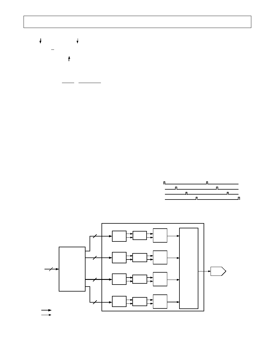
REV. 0
AD6623
37
Time Restriction CMEM Restriction
N
L
RCF
RCF
×
min
1
2
, 16
256
(31)
DMEM Restriction
where:
L
L
L
L
M
N
f
f
RCF
CIC
CIC
CIC
TSP
CLK
IN
=
×
×
=
×
5
2
2
(32)
De-interleaving the input data into multiple TSPs extends the
time restriction and may possibly extend the DMEM restriction,
but will not extend the CMEM restriction. Deinterleaving the
input stream to multiple TSPs divides the input sample rate to
each TSP by the number of TSPs used (N
TSP
). To keep the output
rate fixed, L must be increased by a factor of N
CH
, which extends
the time restriction. This increase in L may be achieved by increas-
ing any one or more of L
RCF
, L
CIC5
, or L
CIC2
within their normal
limits. Achieving a larger L by increasing L
RCF
instead of L
CIC5
or L
CIC2
will relieves the DMEM restriction as well.
In a UMTS example, N
TSP
= 4, f
CLK
= 76.8 MHz, and f
IN
=
3.84 MHz, resulting in L = 80. Factoring L into L
RCF
= 10,
L
CIC
= 8, and L
CIC2
= 1 results in a maximum N
RCF
= 40 due to
the time restriction. Figure 37 shows an example RCF impulse
response which has a frequency response as shown in Figure 38
from 0 Hz to 7.68 MHz (f
IN
L
RCF
/N
TSP
). The composite RCF
and CIC frequency response is shown in Figure 38, on the same
frequency scale. This figure demonstrates a good approximation
to a root-raised-cosine with a roll-off factor of 0.22, a passband
ripple of 0.1 dB, and a stopband ripple better than 70 dB until
the lobe of the first image which peaks at 60 dB about 7.68 MHz
from the carrier center. This lobe could be reduced by shifting
more of the interpolation towards the RCF, but that would
sacrifice near in performance. As shown, the first image can be
easily rejected by an analog filter further up the signal path.
Scaling must be considered as normal with an interpolation
factor of L, to guarantee no overflow in the RCF, CIC, or NCOs.
The output level at the summation port should be calculated
using an interpolation factor of L/N
TSP
.
Programming Multiple TSPs
Configuring the TSPs for de-interleaved operation is straight
forward. All the Channel Registers and the CMEM of each TSP
are programmed identically, except the Start Hold-Off Counters
and NCO Phase Offset.
In order to separate the input timing to each TSP, the Hold-Off
Counters must be used to start each TSP successively in response
to a common Start SYNC. The Start SYNC may originate from
the SYNC pin or the MicroPort. Each subsequent TSP must have
a Hold-Off Counter value L/N
TSP
larger than its predecessor's.
If the TSPs are located on cascaded AD6623s, the Hold-Off
Counters of the upstream device should be incremented by an
additional one.
In the UMTS example, L = 80 and N
TSP
= 4, so to respond as
quickly as possible to a Start SYNC, the Hold-Off Counter
values should be 1, 21, 41, and 61.
Driving Multiple TSP Serial Ports
When configured properly, the AD6623 will drive each SDFO
out of phase. Each new piece of data should be driven only into
the TSP that pulses its SDFO pin at that time.
In the UMTS example in Figure 35, L = 80 and N
TSP
= 4, so
each serial port need only accept every fourth input sample.
Each serial port is shifting at peak capacity, so sample 1, 2, and
3 begin shifting into Serial Ports B, C, and D before sample 0 is
completed into Serial Port A.
SDFOA
SDFOB
SDFOC
SDFOD
0
4
1
5
2
7
6
3
Figure 35. UMTS Example
RAM
COEF
FILTER
CIC
NCO
SUMMATION
BLOCK
CIC
NCO
CIC
NCO
CIC
NCO
DATA
RE-FORMATTER
DAC
RAM
COEF
FILTER
RAM
COEF
FILTER
RAM
COEF
FILTER
76.8 MSAMPLES/SEC
76.8MSPS
76.8MSPS
76.8MSPS
76.8MSPS
9.6MSPS
9.6MSPS
9.6MSPS
9.6MSPS
0.96
MCPS
0.96
MCPS
0.96
MCPS
0.96
MCPS
3.84 MCPS
32
32
32
32
32
I
Q
I
Q
I
Q
I
Q
COMLEX SIGNAL 32 BITS (16, I, 16 Q)
REAL OR IMAGINARY SIGNAL
Figure 36. Summation Block

REV. 0
AD6623
38
COEFFICIENT
1.0
0.5
0
5
MA
GNITUDE
10
0.0
15
20
25
30
35
40
Figure 37. Typical Impulse Response for WBCDMA
kHz
0
1000
dBc
10
0
10
20
30
40
50
60
70
80
90
100
2000 3000 4000 5000 6000 7000 8000 9000 10000
Figure 38. RAM Coefficient Filter, Frequency Response for
WBCDMA
kHz
0
1000
dBc
10
0
10
20
30
40
50
60
70
80
90
100
2000 3000 4000 5000 6000 7000 8000 9000 10000
CIC ROLLOFF
COMPOSITE
AD6623 RESPONSE
IDEAL
FILTER
Figure 39. RCF and CIL, Frequency Response for WBCDMA
THERMAL MANAGEMENT
The power dissipation of the AD6623 is primarily determined
by three factors: the clock rate, the number of channels active,
and the distribution of interpolation rates. The faster the clock
rate the more power dissipated by the CMOS structures of the
AD6623 and the more channels active the higher the overall
power of the chip. Low interpolation rates in the CIC stages
(CIC5, CIC2) results in higher power dissipation. All these
factors should be analyzed as each application has different
thermal requirements.
The AD6623 128-Lead MQFP is specially designed to provide
excellent thermal performance. To achieve the best performance
the power and ground leads should be connected directly to planes
on the PC board. This provides the best thermal transfer from the
AD6623 to the PC board.
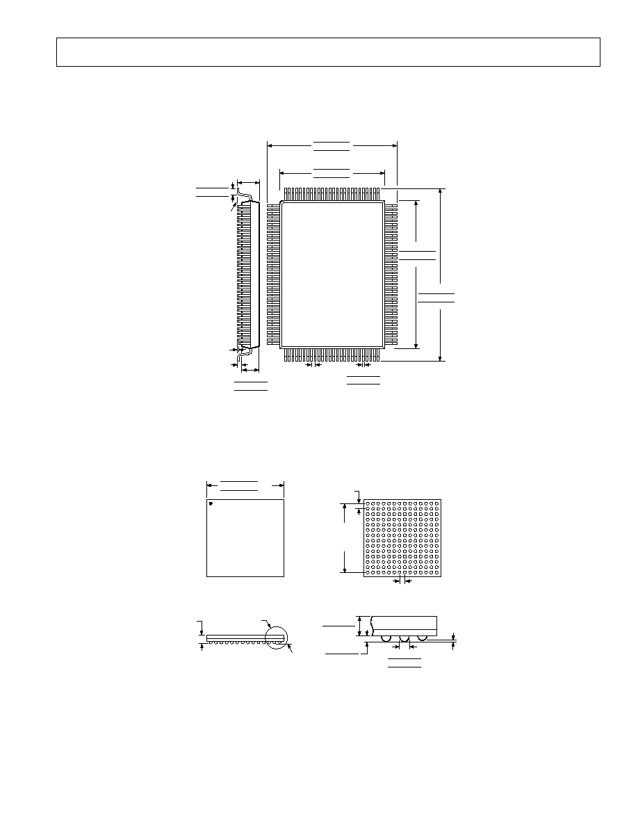
REV. 0
AD6623
39
OUTLINE DIMENSIONS
Dimensions shown in inches and (mm).
128-Lead Terminal Metric Quad Flatpack (MQFP)
TOP VIEW
(PINS DOWN)
1
38
39
65
64
102
128
103
0.011 (0.27)
0.009 (0.22)
0.007 (0.17)
0.020 (0.50)
BSC*
0.555 (14.10)
0.551 (14.00)
0.547 (13.90)
0.685 (17.40)
0.677 (17.20)
0.669 (17.00)
0.791 (20.10)
0.787 (20.00)
0.783 (19.90)
0.921 (23.40)
0.913 (23.20)
0.906 (23.00)
SEATING
PLANE
0.134 (3.40)
MAX
0.041 (1.03)
0.035 (0.88)
0.031 (0.78)
0.003 (0.08)
MAX
0.010 (0.25)
MIN
0.110 (2.80)
0.106 (2.70)
0.102 (2.60)
THE ACTUAL POSITION OF EACH LEAD IS WITHIN 0.00315 (0.08) FROM ITS IDEAL
POSITION WHEN MEASURED IN THE LATERAL DIRECTION. CENTER FIGURES ARE
TYPICAL UNLESS OTHERWISE NOTED
*
196-Lead Ball Grid Array (BGA)
TOP VIEW
0.594 (15.10)
0.591 (15.00) SQ
0.587 (14.90)
BALL A1
INDICATOR
DETAIL A
SEATING
PLANE
0.059
(1.50)
MAX
0.021 (0.53)
0.017 (0.43)
0.008 (0.20)
COPLANARITY
0.028 (0.70)
0.024 (0.60)
0.020 (0.50)
BALL DIAMETER
DETAIL A
0.039 (1.00)
0.033 (0.85)
BOTTOM VIEW
A
B
C
D
E
F
G
H
J
K
L
M
N
P
13
11
9
7
5
3
1
14
12
10
8
6
4
2
0.039 (1.00) BSC
BALL PITCH
0.512
(13.0)
BSC
SQ
0.039 (1.00)
BSC
BALL PITCH
NOTES
1. CONTROLLING DIMENSIONS ARE IN MILLIMETERS
2. THE ACTUAL POSITION OF THE BALL GRID IS WITHIN
0.008 (0.20) OF ITS IDEAL POSITION RELATIVE TO THE
PACKAGE EDGES
3. THE ACTUAL POSITION OF EACH BALL IS WITHIN
0.004 (0.10) OF ITS IDEAL POSITION TO THE BALL GRID
4. CENTER FIGURES ARE NOMINAL DIMENSIONS

40
C0276801/02(0)
PRINTED IN U.S.A.
Document Outline
- Specifications
- Pinout
- Package drawings
- Ordering Guide
- Features
- Applications
- Product Description
- Timing characteristics
- Absolute Maximum Ratings
- Functional Block Diagram
- Pin Function Description
- TABLE OF CONTENTS
- FUNCTIONAL OVERVIEW
- MICROPROCESSOR PORT, MODE INM (MODE = 0)
- MICROPROCESSOR PORT, MOTOROLA (MODE = 1)
- TIMING DIAGRAMS
- TIMING DIAGRAMS-INM MICROPORT MODE
- EXPLANATION OF TEST LEVELS
- CAUTION
- PIN FUNCTION DESCRIPTIONS
- POWER SUPPLY
- INPUTS
- CONTROL
- MICROPORT CONTROL
- OUTPUTS
- JTAG AND BIST
- SERIAL DATA PORT
- PROGRAMMABLE RAM COEFFICIENT FILTER (RCF)
- OVERVIEW OF THE RCF BLOCKS
- INTERPOLATING FIR FILTER
- PSK MODULATOR
- SCALE AND RAMP
- FINE SCALING
- RCF POWER RAMPING
- CASCADED INTEGRATOR COMB (CIC) INTERPOLATING FILTERS
- CIC5
- NUMERICALLY CONTROLLED OSCILLATOR/TUNER (NCO)
- SYNCHRONIZATION
- SCALING
- JTAG INTERFACE
- MICROPORT INTERFACE
- EXTERNAL MEMORY MAP
- INTERNAL COUNTER REGISTERS AND ON-CHIP RAM
- USING THE AD6623 TO PROCESS UMTS CARRIERS
- DIGITAL TO ANALOG CONVERTER (DAC) SELECTION
- THERMAL MANAGEMENT
- DIAGRAMS
- Parallel Output Switching Characteristics
- Wideband Input Timing
- SYNC Timing Inputs Figure 6. SCLK Switching Characteristic (Divide by 2 or EVEN Integer)
- RESET Timing Requirements
- SCLK Switching Characteristics (Divide by 1)
- SCLK Switching Characteristic (Divide by 2 or EVEN Integer)
- SCLK Switching Characteristic (Divide by 3 or ODD Integer)
- Serial Port Timing, Master Mode (SCS = 0), Channel is Self-Framing
- Serial Port Timing, Slave Mode (SCS = 1), Channel is Self-Framing
- Serial Port Timing, Master Mode (SCS = 0), Channel is External-Framing
- Serial Port Timing, Slave Mode (SCS = 1), Channel is External-Framing
- INM Microport Write Timing Requirements
- INM Microport Read Timing Requirements
- MNM Microport Write Timing Requirements
- Motorola Microport Read Timing Requirements
- Serial Port Switching Characteristics
- Data Formats Supported by the AD6623 when SCLK Master (SCS = 0), and SFDO Set for Frame Request (SFE = 0)
- RCF Block Diagram
- Interpolating FIR Filter Block Diagram
- RCF Interpolation
- 16-Phase Modulations
- QPSK Mapper
- PSK Mapper
- þÿ
- Second Order All-Pass IIR Filter
- CIC5
- Numerically Controlled Oscillator and QAM Mixer
- AD6623 Driving Two DACs
- Cascade Operation of Two AD6623s
- NCO Shadow Register and Hold-Off Counter
- Summation Block