 | ÐлекÑÑоннÑй компоненÑ: AD6630PCB | СкаÑаÑÑ:  PDF PDF  ZIP ZIP |
Äîêóìåíòàöèÿ è îïèñàíèÿ www.docs.chipfind.ru
REV. 0
Information furnished by Analog Devices is believed to be accurate and
reliable. However, no responsibility is assumed by Analog Devices for its
use, nor for any infringements of patents or other rights of third parties
which may result from its use. No license is granted by implication or
otherwise under any patent or patent rights of Analog Devices.
a
AD6630
One Technology Way, P.O. Box 9106, Norwood, MA 02062-9106, U.S.A.
Tel: 781/329-4700
World Wide Web Site: http://www.analog.com
Fax: 781/326-8703
© Analog Devices, Inc., 1998
Differential, Low Noise IF Gain
Block with Output Clamping
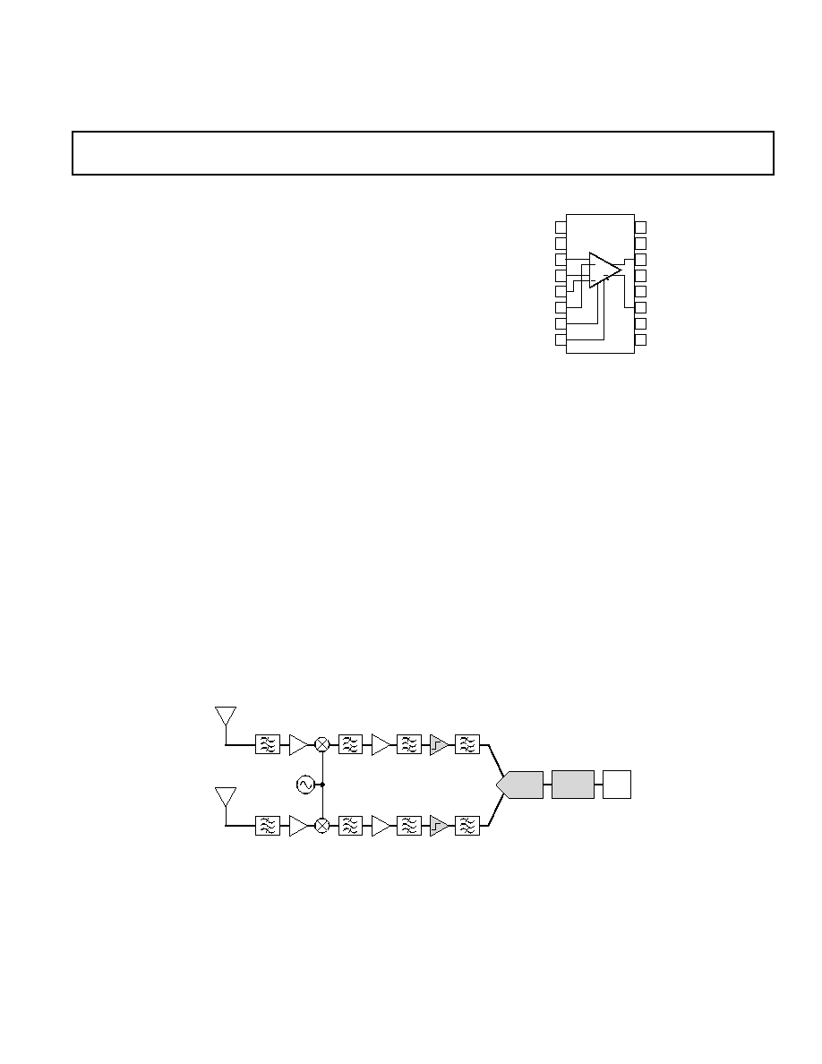
FUNCTIONAL BLOCK DIAGRAM
16
15
14
13
12
11
10
9
1
2
3
4
5
6
7
8
NC = NO CONNECT
NC
V
CC
AD6630
NC
IP2
IP1
IP1
IP2
CLLO
CLHI
CD1
OP
V
EE
CMD
OP
CD2
V
CC
+
+
+
FEATURES
24 dB Gain
4 dB Noise Figure
Easy Match to SAW Filters
Output Limiter Adjustable +8.5 dBm to +12 dBm
700 MHz Bandwidth
10 V Single or Dual 5 V Power Supply
300 mW Power Dissipation
APPLICATIONS
ADC IF Drive Amp
Communications Receivers
PCS/Cellular Base Stations
GSM, CDMA, TDMA
PRODUCT DESCRIPTION
The AD6630 is an IF gain block designed to interface between
SAW filters and differential input analog-to-digital converters.
The AD6630 has a fixed gain of 24 dB and has been optimized
for use with the AD6600 and AD6620 in digitizing narrowband
IF carriers in the 70 MHz to 250 MHz range.
Taking advantage of the differential nature of SAW filters, the
AD6630 has been designed as a differential in/differential out
gain block. This architecture allows 100 dB of adjacent channel
blocking using low cost SAW filters. The AD6630 provides
output limiting for ADC and SAW protection with 10
°
phase
variation in recovery from overdrive situations.
Designed for "narrow-band" cellular/PCS receivers, the high
linearity and low noise performance of the AD6630 allows for
implementation in a wide range of applications ranging from
GSM to CDMA to AMPS. The clamping circuitry also main-
tains the phase integrity of an overdriven signal. This allows
phase demodulation of single carrier signals with an overrange
signal.
While the AD6630 is optimized for use with the AD6600 Dual
Channel, Gain Ranging ADC with RSSI, it can also be used in
many other IF applications. The AD6630 is designed with an
input impedance of 200
and an output of 400
. In the typi-
cal application shown below, these values match the real portion
of a typical SAW filter. Other devices can be matched using
standard matching network techniques.
The AD6630 is built using Analog Devices' high speed comple-
mentary bipolar process. Units are available in a 300 mil SOIC
(16 leads) plastic surface mount package and specified to operate
over the industrial temperature range (40
°
C to +85
°
C).
LOCAL
OSCILLATOR
AD6630
AD6620
DSP
MAIN
DIVERSITY
AD6600
AD6630
AD6620
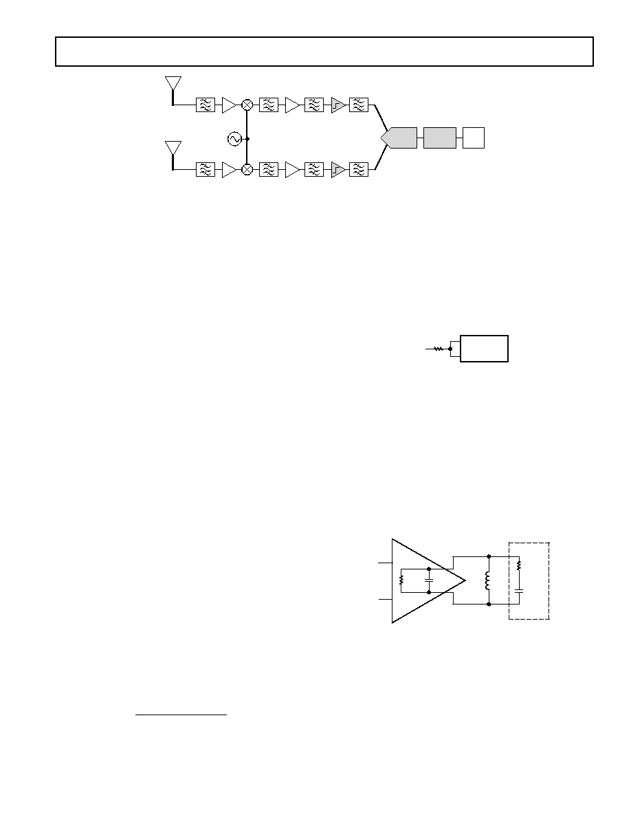
Figure 1. Reference Design
2
REV. 0
AD6630SPECIFICATIONS
NORMAL OPERATING CONDITIONS
Parameter (Conditions)
Min
Typ
Max
Units
SINGLE SUPPLY VOLTAGE
8.5
10.5
V
POSITIVE SUPPLY VOLTAGE
4.25
5.0
5.25
V
NEGATIVE SUPPLY VOLTAGE
5.25
5.0
4.25
V
AMBIENT TEMPERATURE
40
+85
°
C
PACKAGE THERMAL RESISTANCE
80
°
C/W
OPERATING FREQUENCY
1
70
250
MHz
DC SPECIFICATIONS
Test
Parameter
Temp
Level
Min
Typ
Max
Units
SUPPLY CURRENT
Full
II
30
48
mA
OUTPUT DC LEVEL
Full
II
V
M
150
V
M
+150
mV
AC SPECIFICATIONS
Test
Parameter
1
Temp
Level
Min
Typ
Max
Units
GAIN (POWER) @ 70 MHz
Full
II
23
24
25
dB
GAIN (POWER) @ 250 MHz
Full
II
22
23
24
dB
3 dB BANDWIDTH
+25
°
C
V
700
MHz
OUTPUT REFERRED IP3 @ 70 MHz
2
Full
V
22
dBm
OUTPUT REFERRED IP3 @ 250 MHz
2
Full
V
19
dBm
OUTPUT REFERRED IP2 @ 70 MHz
2
Full
V
45
dBm
OUTPUT REFERRED IP2 @ 250 MHz
2
Full
V
45
dBm
OUTPUT REFERRED 1 dB COMPRESSION POINT
@ 70 MHz LOW LEVEL CLAMP
3
Full
II
8.5
dBm
OUTPUT REFERRED 1 dB COMPRESSION POINT
@ 250 MHz LOW LEVEL CLAMP
3
Full
II
7.5
dBm
OUTPUT REFERRED 1 dB COMPRESSION POINT
@ 70 MHz HIGH LEVEL CLAMP
4
Full
II
11
dBm
OUTPUT REFERRED 1 dB COMPRESSION POINT
@ 250 MHz HIGH LEVEL CLAMP
4
Full
II
9
dBm
OUTPUT SLEW RATE
+25
°
C
V
3700
V/
µ
s
INPUT IMPEDANCE (REAL)
+25
°
C
V
200
INPUT CAPACITANCE
+25
°
C
V
2
pF
OUTPUT IMPEDANCE (REAL)
+25
°
C
V
400
OUTPUT CAPACITANCE
+25
°
C
V
2
pF
NOISE FIGURE
+25
°
C
V
4
dB
LOW LEVEL CLAMP MAXIMUM OUTPUT @ 70 MHz
3, 5
Full
IV
11
12.5
dBm
HIGH LEVEL CLAMP MAXIMUM OUTPUT @ 70 MHz
4, 5
Full
IV
13.8
14.3
dBm
LOW LEVEL CLAMP MAXIMUM OUTPUT @ 250 MHz
3, 5
Full
IV
9.25
10.6
dBm
(T
MIN
= 40 C, T
MAX
= +85 C. Output dc levels are nominally at V
M
, where V
M
= V
CC
+ V
EE
= [+5 V + (5 V)] = 0.
Inputs should be AC coupled.)
(T
MIN
= 40 C, T
MAX
= +85 C. All AC production tests are performed at 5 MHz. 70 MHz and 250 MHz
performance limits are correlated to 5 MHz testing based on characterization data.)
3
REV. 0
AD6630
Test
Parameter
Temp
Level
Min
Typ
Max
Units
HIGH LEVEL CLAMP MAXIMUM OUTPUT @ 250 MHz
4, 5
Full
IV
11.2
12.2
dBm
PHASE VARIATION
6
+25
°
C
V
9
Degree
CMRR
7
+25
°
C
V
50
dB
PSRR
8
+25
°
C
V
30
dB
NOTES
1
All specifications are valid across the operating frequency range when the source and load impedance are a conjugate match to the amplifier's input and output
impedance.
2
Test is for two tones separated by 1 MHz for IFs at 70 MHz and 250 MHz at 23 dBm per tone input.
3
Low Level Clamp is selected by connecting pin CLLO to the negative supply, while pin CLHI is left floating. Clamping can be set at lower levels by connecting pin
CLLO and CLHI to the negative supply through an external resistor.
4
High Level Clamp is selected by connecting pin CLHI to the negative supply, while pin CLLO is left floating, this allows the maximum linear range of the device to
be utilized.
5
Output clamp levels are measured for hard clamping with a +3 dBm input level. Valid for a maximum input level of +8 dBm/200
= 3.2 V p-p--differential.
6
Measured as the change in output phase when the input level is changed from 53 dBm to +8 dBm (i.e., from linear operation to clamping).
7
Ratio of the differential output signal (referenced to the input) to the common-mode input signal presented to all input pins.
8
Ratio of signal on supply to differential output (<500 kHz).
Specifications subject to change without notice.
ABSOLUTE MAXIMUM RATINGS
Parameter
Min
Max
Units
Single Supply Voltage
0.5
11.5
V
Positive Supply Voltage
0.5
5.75
V
Negative Supply Voltage
5.75
0.5
V
Input Power
+8
dBm
Storage Temperature
65
+150
°
C
Junction Temperature
+150
°
C
ESD Protection
1
kV
EXPLANATION OF TEST LEVELS
I.
100% production tested.
II.
100% production tested at +25
°
C, and guaranteed by
design and analysis at temperature extremes.
III. Sample tested only.
IV. Parameter guaranteed by design and analysis.
V.
Parameter is typical value only.
VI. 100% production tested at +25
°
C, and sample tested at
temperature extremes.
ORDERING GUIDE
Model
Temperature Range
Package Description
Package Option
AD6630AR
40
°
C to +85
°
C (Ambient)
16-Lead Wide Body SOIC
R-16
AD6630AR-REEL
40
°
C to +85
°
C (Ambient)
AD6630AR on 1000 PC Reel
AD6630R/PCB
Evaluation Board with AD6630AR
CAUTION
ESD (electrostatic discharge) sensitive device. Electrostatic charges as high as 4000 V readily
accumulate on the human body and test equipment and can discharge without detection.
Although the AD6630 features proprietary ESD protection circuitry, permanent damage may
occur on devices subjected to high energy electrostatic discharges. Therefore, proper ESD
precautions are recommended to avoid performance degradation or loss of functionality.
WARNING!
ESD SENSITIVE DEVICE
AD6630
4
REV. 0
PIN FUNCTION DESCRIPTION
Pin No
Pin Name
Description
1, 2
NC
No Connect
3
IP2
Input
4
IP1
Input
5
IP1
Input
6
IP2
Input
7
CLLO
Clamp Level Low Pin
8
CLHI
Clamp Level High Pin
9
V
CC
+V
CC
Supply
10
CD2
Clamp Decoupling
11
OP
Output
12
CMD
DC Feedback Decoupling
13
V
EE
V
EE
Supply
14
OP
Output
15
CD1
Clamp Decoupling
16
V
CC
+V
CC
Supply
PIN CONFIGURATION
TOP VIEW
(Not to Scale)
16
15
14
13
12
11
10
9
1
2
3
4
5
6
7
8
NC
NC
IP2
IP1
IP1
IP2
CLLO
CLHI
V
CC
CD1
OP
V
EE
CMD
OP
CD2
V
CC
AD6630
NC = NO CONNECT
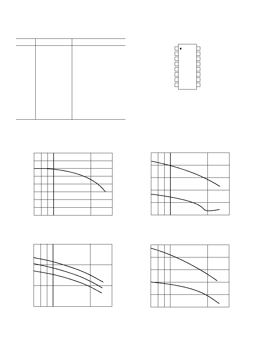
INPUT FREQUENCY MHz
24
70
INTERCEPT POINT dBm
23
22
21
20
100
300
19
18
17
16
Figure 2. 3rd Order Intercept (IP3) vs. Frequency
INPUT FREQUENCY MHz
25
70
GAIN dB
24
23
100
300
22
40 C
+25 C
+85 C
Figure 3. Gain vs. Frequency
Typical Performance Characteristics
INPUT FREQUENCY MHz
13
70
1dB COMPRESSION POINT
12
11
10
9
100
300
8
LOW CLAMP
HIGH CLAMP
Figure 4. 1 dB Compression Point (Typical)
INPUT FREQUENCY MHz
14
70
OUTPUT AMPLITUDE dBm
13
12
11
10
100
300
9
LOW CLAMP
HIGH CLAMP
Figure 5. Clamp Level vs. Frequency
AD6630
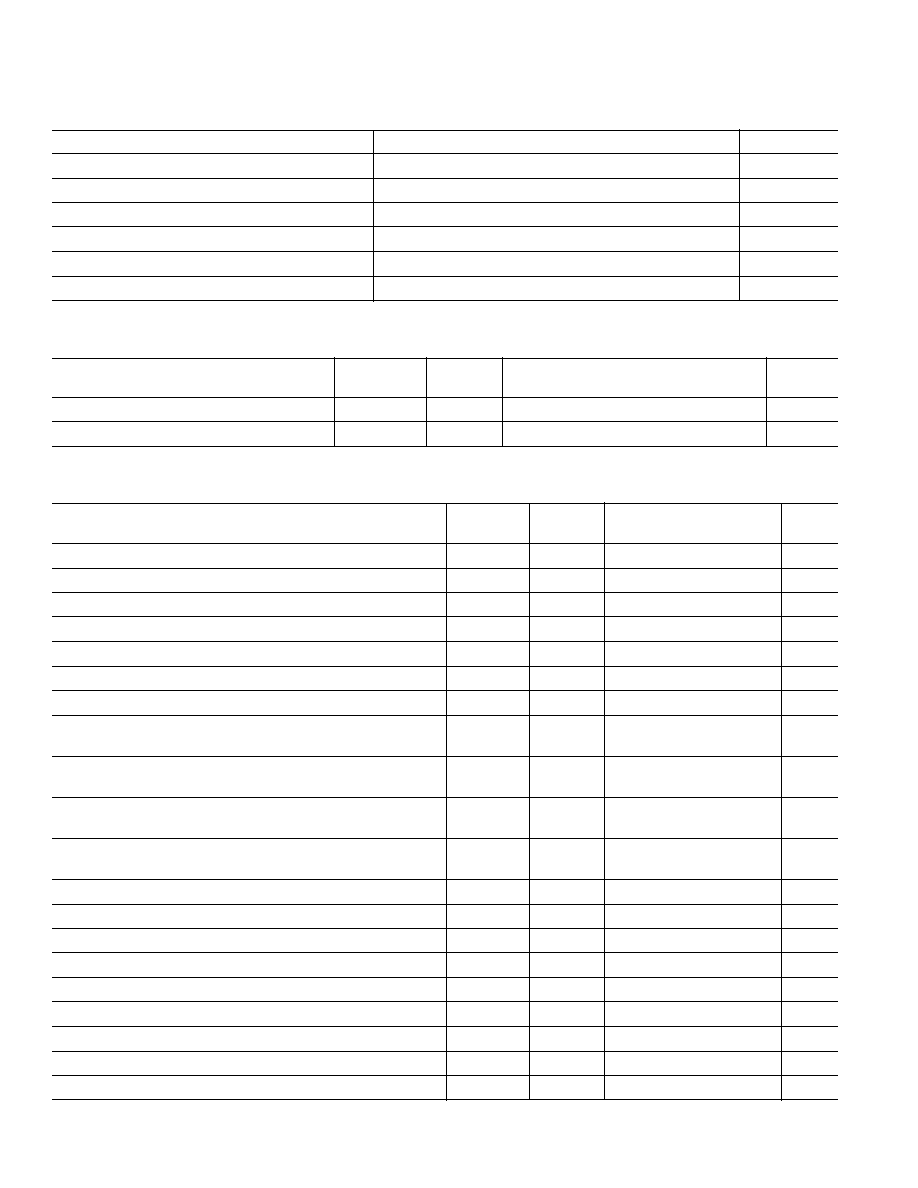
5
REV. 0
AD6630
DSP
MAIN
DIVERSITY
AD6600
28dBm 29dBm 14dBm
LOCAL
OSCILLATOR
23dBm
25dBm10dBm15dBm
9dBm
4dBm
1dB
15dB 9dB
2dB
15dB
5dB
24dB
5dB
SAW
SAW
ANTENNA
104dBm
43dBm
28dBm
16dBm
15dBm
AD6630 INPUT
91dBm
30dBm
15dBm
3dBm
2dBm
AD6630 OUTPUT
67dBm
6dBm
+9dBm
+9dBm
+9dBm
AD6600 INPUT
71dBm
10dBm
+4dBm
+4dBm
+4dBm
AD6620
Figure 6. GSM Design Example
THEORY OF OPERATION
The AD6630 amplifier consists of two stages of gain. The first
stage is differential. This differential amplifier provides good
common-mode rejection to common-mode signals passed by
the SAW filter. The second stage consists of matched current
feedback amplifiers on each side of the differential pair. These
amplifiers provide additional gain as well as output drive capa-
bility. Gain set resistors for these stages are internal to the de-
vice and cannot be changed, allowing fixed compensation for
optimum performance.
Clamping levels for the device are normally set by tying CLLO
or CLHI pins to the negative supply. This internally sets bias
points that generate symmetric clamping levels. Clamping is
achieved primarily in the output amplifiers. Additional input
stage clamping is provided for additional protection. Clamping
levels may be adjusted to lower levels as discussed below.
APPLICATIONS
The AD6630 provides several useful features to meet the needs
of radio designers. The gain and low noise figure of the device
make it perfect for providing interstage gain between differential
SAW filters and/or analog-to-digital converters (ADC). Addi-
tionally, the on-board clamping circuitry provides protection for
sensitive SAW filters or ADCs. The fast recovery of the clamp
circuit permits demodulation of constant envelope modulated
IF signals by preserving the phase response during clamping.
The following topics provide recommendations for using the
AD6630 in narrowband, single carrier applications.
Adjusting Output Clamp Levels
Normally, the output clamp level is set by tying either CLLO or
CLHI to ground or V
EE
. It is possible to set the limit between
8.5 dBm and 12 dBm levels by selecting the appropriate exter-
nal resistor.
To set to a different level, CLLO and CLHI should be tied
together and then through a resistor to ground. The value of the
resistor can be selected using the following equation.
R
OUTPUT
dBm
CLAMP
=
14 4
0 0014
.
.
(
)
This equation is derived from measured data at 170 MHz. Clamp
levels vary with frequency, see Figure 5. Output clamp levels
less than 8.5 dBm will result in damage to the clamp circuitry
unless the absolute maximum input power is derated. Similarly,
the output clamp level cannot be set higher than 12 dBm.
CLAMP
GENERATOR
R
V
EE
Figure 7. Clamp Level Resistor
Matching SAW Filters
The AD6630 is designed to easily match to SAW filters. SAW
filters are largely capacitive in nature. Normally a conjugate
match to the load is desired for maximum power transfer.
Another way to treat the problem is to make the SAW filter look
purely resistive. If the SAW filter load looks resistive there is no
lead or lag in the current vs. voltage. This may not preserve
maximum power transfer, but maximum voltage swing will
exist. All that is required to make the SAW filter input or output
look real is a single inductor shunted across the input. When the
correct value is used, the impedance of the SAW filter becomes
real.
400
3pF
47nH
9.7
15.2pF
Figure 8. Saw Filter Model (170 MHz)
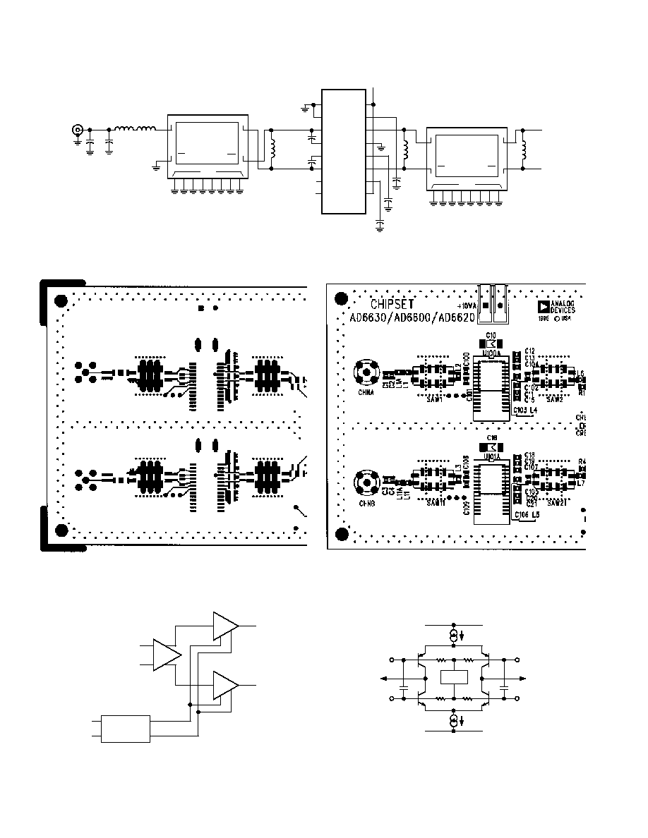
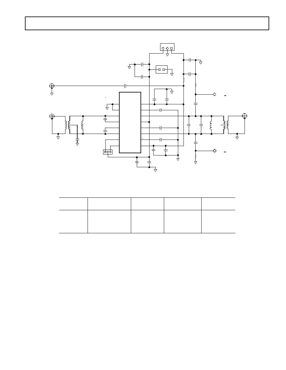
EVALUATION BOARD
Figures 9, 10 and 12 refer to the schematic and layout of the
AD6630AR as used on Analog Devices' GSM Diversity Re-
ceiver Reference Design (only the IF section is shown). Figure
14 references the schematic of the stand-alone AD6630 evalua-
tion board and uses a similar layout. The evaluation board uses
center tapped transformers to convert the input to a differential
signal and AD6630 outputs to a single connector to simplify
evaluation. C8, C9 and L2 are optional reactive components to
tune the load for a particular IF frequency if desired.
AD6630
6
REV. 0
NC1
NC2
IP2
IP1
IP1B
IP2B
CL1
CL2
CD1
OP
CMD
OPB
CD2
V
CC
1
V
EE
V
CC
2
C102
0.1 F
C103
0.1 F
C104
0.1 F
L4
11
12
V
O
V
I
V
O
V
I
SAW2
5
6
GND
1
2
3 4 7 8 9 10
L6
TO
AD6600
C100
0.1 F
C101
0.1 F
L2
11
12
5
6
C2
C1
L1A
L1
SMA
CHNA
+10V
U100A
AD6630
V
O
V
I
V
O
V
I
SAW1
GND
1
2
3 4 7 8 9 10
Figure 9. Reference Design Schematic (One Channel)
Figure 10. Reference Design PCB Layout
CLAMP
GENERATOR
CLP
CLN
CLLO
CLHI
+
DIFF
AMP
+
OUTPUT
AMP
OUTPUT
AMP
+
Figure 11. Functional Block Diagram
Figure 12. Reference Design Component Placement (Two
Channels Shown)
TO OUTPUT
AMPLIFIER
TO OUTPUT
AMPLIFIER
V
EE
V
CC
200
200
200
200
IP1
IP2
IP1
IP2
BIAS
Figure 13. Equivalent Input Circuit
AD6630
7
REV. 0
Table I. Typical S Parameters
Frequency
(MHz)
S
11
S
12
S
21
S
22
70
224.5
4.52
°
41.0
3.0
°
24.1
8.8
°
394.3
8.6
°
170
264.8
32.9
°
31.4
0
°
23.5
22.5
°
382.4
21.9
°
200
227.9
34.8
°
41.0
5
°
23.2
26.4
°
353.0
25.4
°
250
209.5
36.2
°
40.6
2.3
°
22.9
38.9
°
328.9
29.2
°
AGND
J3
11
2
C21
10nF
+
AGND
1
AGND
C15
1nF
C10
100nF
R1
200
AGND
2
C13
1 F
C16
10nF
+
1
AGND
C17
10nF
J1
PCTB3
C2
10nF
TP1
TEST P
1
2
3
AGND
TP2
TEST P
J6
SMA
J7
SMA
1
2
4
6
AGND
1
2
3
C1
10nF
L1
470nH
AGND
C12
10nF
C11
10nF
AGND
1
2
3
4
5
6
7
8
10
11
12
13
14
15
16
AD6630
U1
J2
NC1
NC2
IP2
IP1
IP1B
IP2B
CL1
CL2
V
CC
1
CD1
OP
V
EE
C20
1nF
C19
100nF
AGND
AGND
C14
1nF
C4
100nF
C6
C7
C5
10nF
10nF
10nF
C8
C9
L2
T2
TC 8-1
AT224
AGND
2
1
T1
TC41W
AT224
J8
SMA
C3
10nF
R3
R2
200
C18
1 F
9
CMD
OPB
CD2
V
CC
2
1
2
1
4
6
1
2
3
Figure 14. Evaluation Board Schematic
AD6630
8
REV. 0
C3412810/98
PRINTED IN U.S.A.
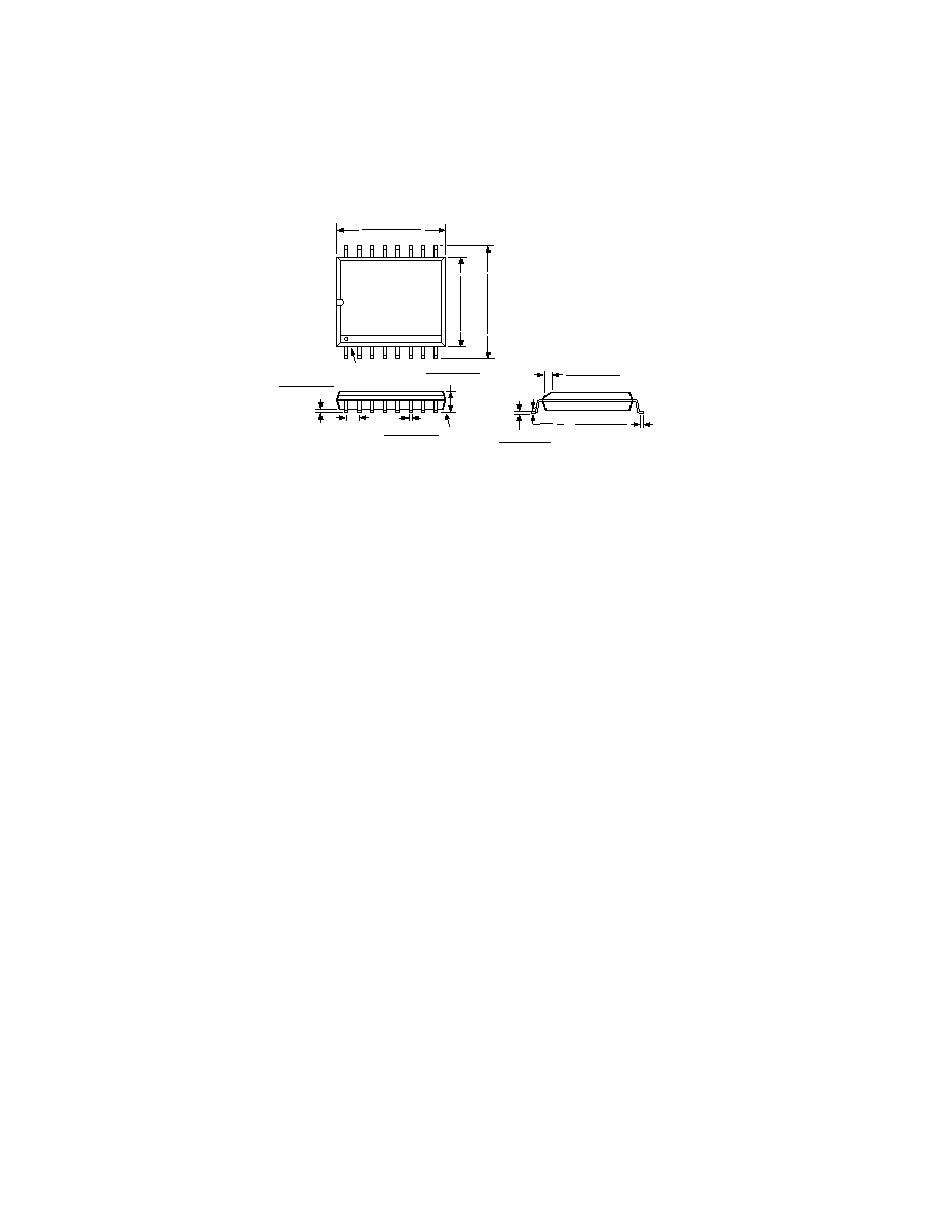
OUTLINE DIMENSIONS
Dimensions shown in inches and (mm).
16-Lead Wide Body SOIC
(R-16)
0.2992 (7.60)
0.2914 (7.40)
16
9
8
1
0.4133 (10.50)
0.3977 (10.00)
0.4193 (10.65)
0.3937 (10.00)
PIN 1
SEATING
PLANE
0.0118 (0.30)
0.0040 (0.10)
0.0192 (0.49)
0.0138 (0.35)
0.1043 (2.65)
0.0926 (2.35)
0.0500
(1.27)
BSC
0.0125 (0.32)
0.0091 (0.23)
0.0500 (1.27)
0.0157 (0.40)
0.0291 (0.74)
0.0098 (0.25)
x 45
8
0