Äîêóìåíòàöèÿ è îïèñàíèÿ www.docs.chipfind.ru
a
Information furnished by Analog Devices is believed to be accurate and
reliable. However, no responsibility is assumed by Analog Devices for its
use, nor for any infringements of patents or other rights of third parties that
may result from its use. No license is granted by implication or otherwise
under any patent or patent rights of Analog Devices.
One Technology Way, P.O. Box 9106, Norwood, MA 02062-9106, U.S.A.
Tel: 781/329-4700
www.analog.com
Fax: 781/326-8703
© Analog Devices, Inc., 2002
AD6645
14-Bit, 80 MSPS
A/D Converter
REV. 0
FEATURES
80 MSPS Guaranteed Sample Rate
SNR = 75 dB, f
IN
15 MHz @ 80 MSPS
SNR = 72 dB, f
IN
200 MHz @ 80 MSPS
SFDR = 89 dBc, f
IN
70 MHz @ 80 MSPS
100 dB Multitone SFDR
IF Sampling to 200 MHz
Sampling Jitter 0.1 ps
1.5 W Power Dissipation
Differential Analog Inputs
Pin-Compatible to AD6644
Two's Complement Digital Output Format
3.3 V CMOS-Compatible
DataReady for Output Latching
APPLICATIONS
Multichannel, Multimode Receivers
Base Station Infrastructure
AMPS, IS-136, CDMA, GSM, WCDMA
Single Channel Digital Receivers
Antenna Array Processing
Communications Instrumentation
Radar, Infrared Imaging
Instrumentation
PRODUCT DESCRIPTION
The AD6645 is a high-speed, high-performance, monolithic
14-bit analog-to-digital converter. All necessary functions,
including track-and-hold (T/H) and reference, are included on
the chip to provide a complete conversion solution. The AD6645
provides CMOS-compatible digital outputs. It is the fourth
generation in a wideband ADC family, preceded by the
AD9042 (12-bit, 41 MSPS), the AD6640 (12-bit, 65 MSPS,
IF sampling), and the AD6644 (14-bit, 40 MSPS/65 MSPS).
Designed for multichannel, multimode receivers, the AD6645 is
part of Analog Device's SoftCellTM transceiver chipset. The
AD6645 maintains 100 dB multitone, spurious-free dynamic
range (SFDR) through the second Nyquist band. This break-
through performance eases the burden placed on multimode
digital receivers (software radios) that are typically limited by
the ADC. Noise performance is exceptional; typical signal-to-
noise ratio is 74.5 dB through the first Nyquist band.
The AD6645 is built on Analog Devices' high-speed complemen-
tary bipolar process (XFCB) and uses an innovative, multipass
circuit architecture. Units are available in a thermally enhanced 52-
lead PowerQuad 4
®
(LQFP_ED) specified from 40
C to +85C.
PRODUCT HIGHLIGHTS
1. IF Sampling
The AD6645 maintains outstanding ac performance up to
input frequencies of 200 MHz. Suitable for multicarrier 3G
wideband cellular IF sampling receivers.
2. Pin Compatibility
The ADC has the same footprint and pin layout as the
AD6644, 14-Bit 40 MSPS/65 MSPS ADC.
3. SFDR Performance and Oversampling
Multitone SFDR performance of 100 dBc can reduce the
requirements of high-end RF components and allows the use
of receive signal processors such as the AD6620 or AD6624/
AD6624A.
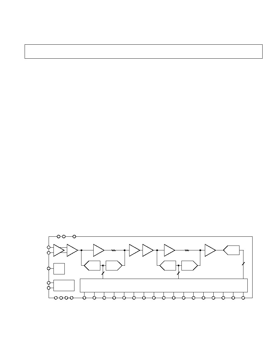
FUNCTIONAL BLOCK DIAGRAM
5
A1
TH2
A2
TH4
ADC3
TH5
TH3
TH1
DAC1
ADC2
DAC2
ADC1
6
AIN
AIN
VREF
ENCODE
ENCODE
AV
CC
DV
CC
GND
DMID
OVR
DRY
D13
MSB
D12
D11
D10
D9
D8
D7
D6
D5
D4
D3
D2
D1
D0
LSB
INTERNAL
TIMING
5
DIGITAL ERROR CORRECTION LOGIC
AD6645
2.4V
SoftCell is a trademark of Analog Devices, Inc.
PowerQuad 4 is a registered trademark of Amkor Technology, Inc.

REV. 0
2
AD6645
DC SPECIFICATIONS
AD6645ASQ-80
Parameter
Temp
Test Level
Min
Typ
Max
Unit
RESOLUTION
14
Bits
ACCURACY
No Missing Codes
Full
II
Guaranteed
Offset Error
Full
II
10
+1.2
+10
mV
Gain Error
Full
II
10
0
+10
% FS
Differential Nonlinearity (DNL)
Full
II
1.0
±0.25
+1.5
LSB
Integral Nonlinearity (INL)
Full
V
±0.5
LSB
TEMPERATURE DRIFT
Offset Error
Full
V
1.5
ppm/
C
Gain Error
Full
V
48
ppm/
C
POWER SUPPLY REJECTION (PSRR)
25
C
V
±1.0
mV/V
REFERENCE OUT (VREF)
1
Full
V
2.4
V
ANALOG INPUTS (AIN,
AIN)
Differential Input Voltage Range
Full
V
2.2
V p-p
Differential Input Resistance
Full
V
1
k
W
Differential Input Capacitance
25
C
V
1.5
pF
POWER SUPPLY
Supply Voltages
AV
CC
Full
II
4.75
5.0
5.25
V
DV
CC
Full
II
3.0
3.3
3.6
V
Supply Current
I AV
CC
(AV
CC
= 5.0 V)
Full
II
275
320
mA
I DV
CC
(DV
CC
= 3.3 V)
Full
II
32
45
mA
Rise Time
2
AV
CC
Full
IV
TBD
ms
POWER CONSUMPTION
Full
II
1.5
1.75
W
NOTES
1
VREF is provided for setting the common-mode offset of a differential amplifier such as the AD8138 when a dc-coupled analog input is required. VREF should be
buffered if used to drive additional circuit functions.
2
Specified for dc supplies with linear rise-time characteristics. The use of dc supplies with linear rise-times of <45 ms is highly recommended.
Specifications subject to change without notice
DIGITAL SPECIFICATIONS
AD6645ASQ-80
Parameter (Conditions)
Temp
Test Level
Min
Typ
Max
Unit
ENCODE INPUTS (ENC,
ENC)
Differential Input Voltage
1
Full
IV
0.4
V p-p
Differential Input Resistance
25
C
V
10
k
W
Differential Input Capacitance
25
C
V
2.5
pF
LOGIC OUTPUTS (D13D0, DRY, OVR
2
)
Logic Compatibility
CMOS
Logic "1" Voltage (DV
CC
= 3.3 V)
3
Full
II
2.85
DV
CC
0.2
V
Logic "0" Voltage (DV
CC
= 3.3 V)
3
Full
II
0.2
0.5
V
Output Coding
Two's Complement
DMID
Full
V
DV
CC
/2
V
NOTES
1
All ac specifications tested by driving ENCODE and
ENCODE differentially.
2
The functionality of the Over-Range bit is specified for a temperature range of 25
C to 85C only.
3
Digital output logic levels: DV
CC
= 3.3 V, C
LOAD
= 10 pF. Capacitive loads >10 pF will degrade performance.
Specifications subject to change without notice.
(AV
CC
= 5 V, DV
CC
= 3.3 V; T
MIN
= 40 C, T
MAX
= +85 C, unless otherwise noted.)
(AV
CC
= 5 V, DV
CC
= 3.3 V; T
MIN
= 40 C, T
MAX
= +85 C, unless otherwise noted.)
SPECIFICATIONS

REV. 0
3
AD6645
AC SPECIFICATIONS
1
AD6645ASQ-80
Parameter (Conditions)
Temp
Test Level
Min
Typ
Max
Unit
SNR
Analog Input
15.5 MHz
25
C
V
75.0
dB
@ 1 dBFS
30.5 MHz
25
C
II
72.5
74.5
dB
70.0 MHz
25
C
II
72.0
73.5
dB
150.0 MHz
25
C
V
73.0
dB
200.0 MHz
25
C
V
72.0
dB
SINAD
Analog Input
15.5 MHz
25
C
V
75.0
dB
@ 1 dBFS
30.5 MHz
25
C
II
72.5
74.5
dB
70.0 MHz
25
C
V
73.0
dB
150.0 MHz
25
C
V
68.5
dB
200.0 MHz
25
C
V
62.5
dB
WORST HARMONIC (2
nd
or 3
rd
)
Analog Input
15.5 MHz
25
C
V
93.0
dBc
@ 1 dBFS
30.5 MHz
25
C
II
85.0
93.0
dBc
70.0 MHz
25
C
V
89.0
dBc
150.0 MHz
25
C
V
70.0
dBc
200.0 MHz
25
C
V
63.5
dBc
WORST HARMONIC (4
th
or H
IGHER
)
Analog Input
15.5 MHz
25
C
V
96.0
dBc
@ 1 dBFS
30.5 MHz
25
C
II
85.0
95.0
dBc
70.0 MHz
25
C
V
90.0
dBc
150.0 MHz
25
C
V
90.0
dBc
200.0 MHz
25
C
V
88.0
dBc
TWO TONE SFDR @ 30.5 MHz
2, 3
25
C
V
100
dBFS
55.0 MHz
2, 4
25
C
V
100
dBFS
TWO TONE IMD REJECTION
3, 4
F1, F2 @ 7 dBFS
25
C
V
90
dBc
ANALOG INPUT BANDWIDTH
25
C
V
270
MHz
NOTES
1
All ac specifications tested by driving ENCODE and
ENCODE differentially.
2
Analog input signal power swept from 10 dBFS to 100 dBFS.
3
F1 = 30.5 MHz, F2 = 31.5 MHz.
4
F1 = 55.25 MHz, F2 = 56.25 MHz.
Specifications subject to change without notice.
SWITCHING SPECIFICATIONS
AD6645ASQ-80
Parameter (Conditions)
Temp
Test Level
Min
Typ
Max
Unit
Maximum Conversion Rate
Full
II
80
MSPS
Minimum Conversion Rate
Full
IV
30
MSPS
ENCODE Pulsewidth High (t
ENCH
)
*
Full
IV
5.625
ns
ENCODE Pulsewidth Low (t
ENCL
)
*
Full
IV
5.625
ns
*Several timing parameters are a function of t
ENCL
and t
ENCH
.
Specifications subject to change without notice.
(AV
CC
= 5 V, DV
CC
= 3.3 V; ENCODE and
ENCODE = 80 MSPS; T
MIN
= 40 C, T
MAX
= +85 C, unless
otherwise noted.)
(AV
CC
= 5 V, DV
CC
= 3.3 V; ENCODE and
ENCODE = 80 MSPS; T
MIN
= 40 C, T
MAX
= +85 C, unless
otherwise noted.)
REV. 0
AD6645
4
SWITCHING SPECIFICATIONS
(continued)
AD6645ASQ-80
Parameter (Conditions)
Name
Temp
Test Level
Min
Typ
Max
Unit
ENCODE Input Parameters
1
Encode Period
1
@ 80 MSPS
t
ENC
Full
V
12.5
ns
Encode Pulsewidth High
2
@ 80 MSPS
t
ENCH
Full
V
6.25
ns
Encode Pulsewidth Low @ 80 MSPS
t
ENCL
Full
V
6.25
ns
ENCODE/DataReady
Encode Rising to DataReady Falling
t
DR
Full
V
1.0
2.0
3.1
ns
Encode Rising to DataReady Rising
t
E_DR
Full
V
t
ENCH
+ t
DR
ns
@ 80 MSPS (50% Duty Cycle)
Full
V
7.3
8.3
9.4
ns
ENCODE/DATA (D13:0), OVR
ENC to DATA Falling Low
t
E_FL
Full
V
2.4
4.7
7.0
ns
ENC to DATA Rising Low
t
E_RL
Full
V
1.4
3.0
4.7
ns
ENCODE to DATA Delay (Hold Time)
3
t
H_E
Full
V
1.4
3.0
4.7
ns
ENCODE to DATA Delay (Setup Time)
4
t
S_E
Full
V
t
ENC
t
E_FL
ns
Encode = 80 MSPS (50% Duty Cycle)
Full
V
5.3
7.6
10.0
ns
DataReady (DRY
5
)/DATA, OVR
DataReady to DATA Delay (Hold Time)
2
t
H_DR
Full
V
Note 6
ns
Encode = 80 MSPS (50% Duty Cycle)
6.6
7.2
7.9
DataReady to DATA Delay (Setup Time)
2
t
S_DR
Full
V
Note 6
ns
Encode = 80 MSPS (50% Duty Cycle)
2.1
3.6
5.1
APERTURE DELAY
t
A
25
C
V
500
ps
APERTURE UNCERTAINTY (Jitter)
t
J
25
C
V
0.1
ps rms
NOTES
1
Several timing parameters are a function of t
ENC
and t
ENCH
.
2
To compensate for a change in duty cycle for t
H_DR
and t
S_DR
use the following equation:
Newt
H_DR
= (t
H_DR
% Change(t
ENCH
))
Newt
S_DR
= (t
S_DR
% Change(t
ENCH
))
3
ENCODE TO DATA Delay (Hold Time) is the absolute minimum propagation delay through the Analog-to-Digital Converter, t
E_RL
= t
H_E
.
4
ENCODE TO DATA Delay (Setup Time) is calculated relative to 80 MSPS (50% duty cycle). To calculate t
S_E
for a given encode, use the following equation:
Newt
S_E
= t
ENC(NEW)
t
ENC
+ t
S_E
(i.e., for 40 MSPS: Newt
S_E(TYP)
= 25
¥ 10
9
15.38
¥ 10
9
+ 9.8
¥ 10
9
= 19.4
¥ 10
9
).
5
DRY is an inverted and delayed version of the encode clock. Any change in the duty cycle of the clock will correspondingly change the duty cycle of DRY.
6
DataReady to DATA Delay (t
H_DR
and t
S_DR
) is calculated relative to 80 MSPS (50% duty cycle) and is dependent on t
ENC
and duty cycle. To calculate t
H_DR
and
t
S_DR
for a given encode, use the following equations:
Newt
H_DR
= t
ENC(NEW)
/2 t
ENCH
+ t
H_DR
(i.e., for 40 MSPS: Newt
H_DR(TYP)
= 12.5
¥ 10
9
6.25
¥ 10
9
+ 7.2
¥ 10
9
= 13.45
¥ 10
9
Newt
S_DR
= t
ENC(NEW)
/2 t
ENCH
+ t
S_DR
(i.e., for 40 MSPS: Newt
S_DR(TYP)
= 12.5
¥ 10
9
6.25
¥ 10
9
+ 3.6
¥ 10
9
= 9.85
¥ 10
9
Specifications subject to change without notice.
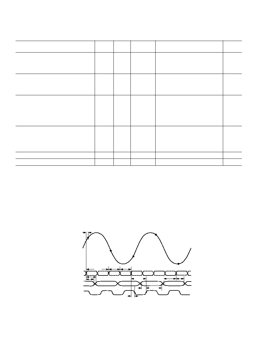
t
S_DR
t
A
AIN
N
N+1
N+2
N+3
N+4
t
ENC
t
ENCH
t
ENCL
t
E_FL
t
E_RL
t
E_DR
t
S_E
t
H_E
t
DR
t
H_DR
N
N+1
N+2
N+3
N+4
N
N1
N2
N3
ENC, ENC
D[13:0], OVR
DRY
Figure 1. Timing Diagram
(AV
CC
= 5 V, DV
CC
= 3.3 V; ENCODE and
ENCODE = 80 MSPS; T
MIN
= 40 C,
T
MAX
= +85 C, C
LOAD
= 10 pF, unless otherwise noted.)
REV. 0
5
AD6645
ABSOLUTE MAXIMUM RATINGS
*
Parameter
Min
Max
Unit
ELECTRICAL
AV
CC
Voltage
0
7
V
DV
CC
Voltage
0
7
V
Analog Input Voltage
0
AV
CC
V
Analog Input Current
25
mA
Digital Input Voltage
0
AV
CC
V
Digital Output Current
4
mA
ENVIRONMENTAL
Operating Temperature Range (Ambient)
40
+85
C
Maximum Junction Temperature
150
C
Lead Temperature (Soldering, 10 sec)
300
C
Storage Temperature Range (Ambient)
65
+150
C
THERMAL CHARACTERISTICS
52-Lead PowerQuad 4 . . . . . . . . . . . . . . . . . . . . . . LQFP_ED
JA
= 23
C/W . . . . . . . . . . . . . . . Soldered Slug, No Airflow
JA
= 17
C/W . . . . . . . . Soldered Slug, 200 LFPM Airflow
JA
= 30
C/W . . . . . . . . . . . . . Unsoldered Slug, No Airflow
JA
= 24
C/W . . . . . . Unsoldered Slug, 200 LFPM Airflow
JC
= 2
C/W . . . . . . . . . . . . . Bottom of Package (Heatslug)
Typical Four-Layer JEDEC Board Horizontal Orientation
CAUTION
ESD (electrostatic discharge) sensitive device. Electrostatic charges as high as 4000 V readily
accumulate on the human body and test equipment and can discharge without detection. Although
the AD6645 features proprietary ESD protection circuitry, permanent damage may occur on
devices subjected to high-energy electrostatic discharges. Therefore, proper ESD precautions are
recommended to avoid performance degradation or loss of functionality.
WARNING!
ESD SENSITIVE DEVICE
EXPLANATION OF TEST LEVELS
Test Level
I.
100% production tested.
II.
100% production tested at 25
C and guaranteed by design
and characterization at temperature extremes.
III. Sample tested only.
IV. Parameter is guaranteed by design and characterization
testing.
V.
Parameter is a typical value only.
*Absolute maximum ratings are limiting values to be applied individually and beyond which the serviceability
of the circuit may be impaired. Functional operability is not necessarily implied. Exposure to absolute
maximum rating conditions for an extended period of time may affect device reliability.
ORDERING GUIDE
Model
Temperature Range
Package Description
Package Option
AD6645ASQ-80
40
C to +85C (Ambient) 52-Lead PowerQuad 4 (LQFP_ED) SQ-52
AD6645/PCB
25
C
Evaluation Board
REV. 0
AD6645
6
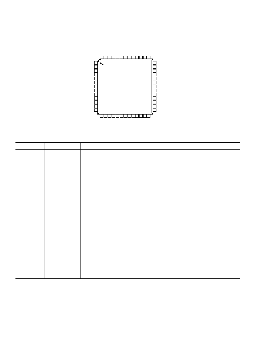
PIN CONFIGURATION
52 51 50 49 48
43 42 41 40
47 46 45 44
14 15 16 17 18 19 20 21 22 23 24 25 26
1
2
3
4
5
6
7
8
9
10
11
13
12
PIN 1
IDENTIFIER
TOP VIEW
(Not to Scale)
39
38
37
36
35
34
33
32
31
30
29
28
27
AD6645
AV
CC
GND
AV
CC
GND
AV
CC
GND
GND
AV
CC
GND
C2
GND
AV
CC
DRY
D13 (MSB)
D12
D11
D10
D9
D8
D7
DV
CC
GND
D5
D4
DV
CC
GND
VREF
GND
ENC
ENC
GND
AV
CC
AV
CC
GND
AIN
AIN
GND
D3
D2
D1
D0 (LSB)
DMID
GND
DV
CC
OVR
DNC
AV
CC
GND
AV
CC
GND
C1
D6
DNC = DO NOT CONNECT
PIN FUNCTION DESCRIPTIONS
Pin No.
Mnemonic
Function
1, 33, 43
DV
CC
3.3 V Power Supply (Digital) Output Stage Only
2, 4, 7, 10, 13,
GND
Ground
15, 17, 19, 21,
23, 25, 27, 29,
34, 42
3
VREF
2.4 V Reference. Bypass to ground with a 0.1
mF microwave chip capacitor.
5
ENC
Encode Input. Conversion initiated on rising edge.
6
ENC
Complement of ENC, Differential Input
8, 9, 14, 16, 18,
AV
CC
5 V Analog Power Supply
22, 26, 28, 30
11
AIN
Analog Input
12
AIN
Complement of AIN, Differential Analog Input
20
C1
Internal Voltage Reference. Bypass to ground with a 0.1
mF chip capacitor.
24
C2
Internal Voltage Reference. Bypass to ground with a 0.1
mF chip capacitor.
31
DNC
Do not connect this pin.
32
OVR
*
Over-Range Bit. A logic-level high indicates analog input exceeds
±FS.
35
DMID
Output Data Voltage Midpoint. Approximately equal to (DV
CC
)/2.
36
D0 (LSB)
Digital Output Bit (Least Significant Bit); Two's Complement
3741, 4450
D1D5, D6D12
Digital Output Bits in Two's Complement
51
D13 (MSB)
Digital Output Bit (Most Significant Bit); Two's Complement
52
DRY
DataReady Output
*The functionality of the Over-Range bit is specified for a temperature range of 25
C to 85C only.

REV. 0
7
AD6645
DEFINITIONS OF SPECIFICATIONS
Analog Bandwidth
The analog input frequency at which the spectral power of the
fundamental frequency (as determined by the FFT analysis) is
reduced by 3 dB.
Aperture Delay
The delay between the 50% point of the rising edge of the
ENCODE command and the instant at which the analog input
is sampled.
Aperture Uncertainty (Jitter)
The sample-to-sample variation in aperture delay.
Differential Analog Input Resistance, Differential Analog
Input Capacitance, and Differential Analog Input Impedance
The real and complex impedances measured at each analog
input port. The resistance is measured statically and the capaci-
tance and differential input impedances are measured with a
network analyzer.
Differential Analog Input Voltage Range
The peak-to-peak differential voltage that must be applied to
the converter to generate a full-scale response. Peak differential
voltage is computed by observing the voltage on a single pin and
subtracting the voltage from the other pin, which is 180 degrees
out of phase. Peak-to-peak differential is computed by rotating
the inputs phase 180 degrees and taking the peak measurement
again. Then the difference is computed between both peak
measurements.
Differential Nonlinearity
The deviation of any code width from an ideal 1 LSB step.
Encode Pulsewidth/Duty Cycle
Pulsewidth high is the minimum amount of time that the
ENCODE pulse should be left in Logic "1" state to achieve
rated performance; pulsewidth low is the minimum time
ENCODE pulse should be left in low state. See timing implica-
tions of changing t
ENCH
in text. At a given clock rate, these
specs define an acceptable ENCODE duty cycle.
Full-Scale Input Power
Expressed in dBm. Computed using the following equation:
Power
V
Z
Full Scale
Full Scale rms
Input
=
È
Î
Í
Í
Í
Í
Í
ù
û
ú
ú
ú
ú
ú
10
0 001
2
log
| |
.
Harmonic Distortion, 2
nd
The ratio of the rms signal amplitude to the rms value of the
second harmonic component, reported in dBc.
Harmonic Distortion, 3
rd
The ratio of the rms signal amplitude to the rms value of the
third harmonic component, reported in dBc.
Integral Nonlinearity
The deviation of the transfer function from a reference line
measured in fractions of 1 LSB using a "best straight line"
determined by a least square curve fit.
Minimum Conversion Rate
The encode rate at which the SNR of the lowest analog
signal frequency drops by no more than 3 dB below the
guaranteed limit.
Maximum Conversion Rate
The encode rate at which parametric testing is performed.
Noise (For Any Range Within the ADC)
V
Z
NOISE
FS
SNR
Signal
dBm
dBc
dBFS
=
¥
¥
-
Ê
Ë
Á
^
¯
~
|
|
.
0 001 10
10
Where Z is the input impedance, FS is the full scale of the device
for the frequency in question; SNR is the value for the particular
input level; and Signal is the signal level within the ADC reported
in dB below full scale. This value includes both thermal and
quantization noise.
Output Propagation Delay
The delay between a differential crossing of ENCODE and
ENCODE and the time when all output data bits are within
valid logic levels.
Power Supply Rejection Ratio
The ratio of a change in input offset voltage to a change in power
supply voltage.
Power Supply Rise Time
The time from when the dc supply is initiated, until the supply
output reaches the minimum specified operating voltage for the
ADC. The dc level is measured at supply pin(s) of the ADC.
Signal-to-Noise-and-Distortion (SINAD)
The ratio of the rms signal amplitude (set 1 dB below full scale)
to the rms value of the sum of all other spectral components,
including harmonics but excluding dc.
Signal-to-Noise Ratio (without Harmonics)
The ratio of the rms signal amplitude (set at 1 dB below full
scale) to the rms value of the sum of all other spectral compo-
nents, excluding the first five harmonics and dc.
Spurious-Free Dynamic Range (SFDR)
The ratio of the rms signal amplitude to the rms value of the peak
spurious spectral component. The peak spurious component
may or may not be a harmonic. May be reported in dBc (i.e.,
degrades as signal level is lowered) or dBFS (always related
back to converter full scale).
Two Tone Intermodulation Distortion Rejection
The ratio of the rms value of either input tone to the rms value of
the worst third order intermodulation product; reported in dBc.
Two Tone SFDR
The ratio of the rms value of either input tone to the rms value
of the peak spurious component. The peak spurious component
may or may not be an IMD product. May be reported in dBc
(i.e., degrades as signal level is lowered) or in dBFS (always
related back to converter full scale).
Worst Other Spur
The ratio of the rms signal amplitude to the rms value of the
worst spurious component (excluding the second and third
harmonic) reported in dBc.
REV. 0
AD6645
8
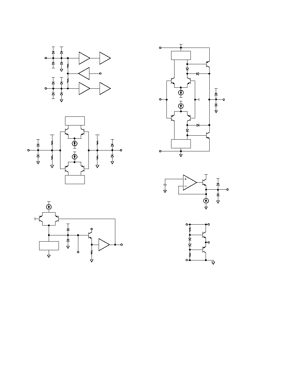
EQUIVALENT CIRCUITS
BUF
T/H
BUF
BUF
T/H
V
CH
AV
CC
500
V
CL
AIN
V
CH
AV
CC
V
CL
AIN
500
V
REF
Figure 2. Analog Input Stage
LOADS
LOADS
10k
10k
10k
10k
ENC
ENC
AV
CC
AV
CC
AV
CC
AV
CC
Figure 3. Encode Inputs
AV
CC
CURRENT
MIRROR
V
REF
AV
CC
AV
CC
C1, C2
Figure 4. Compensation Pin, C1 or C2
CURRENT
MIRROR
CURRENT
MIRROR
V
REF
D0D13,
OVR, DRY
DV
CC
DV
CC
Figure 5. Digital Output Stage
AV
CC
AV
CC
V
REF
100 A
2.4V
Figure 6. 2.4 V Reference
10k
DMID
10k
DV
CC
Figure 7. DMID Reference
REV. 0
9
AD6645
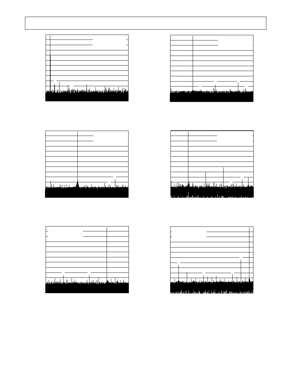
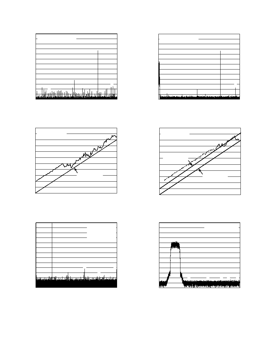
FREQUENCY MHz
130
0
5
10
15
20
25
30
35
40
120
110
100
90
80
70
60
50
40
30
20
10
0
ENCODE = 80MSPS
AIN = 2.2MHz @ 1dBFS
SNR = 75.0dB
SFDR = 93.0dBc
dBFS
2
6
5
4
3
TPC 1. Single Tone @ 2.2 MHz
FREQUENCY MHz
130
0
5
10
15
20
25
30
35
40
120
110
100
90
80
70
60
50
40
30
20
10
0
dBFS
2
6
5
4
3
ENCODE = 80MSPS
AIN = 15.5MHz @ 1dBFS
SNR = 75.0dB
SFDR = 93.0dBc
TPC 2. Single Tone @ 15.5 MHz
FREQUENCY MHz
130
0
5
10
15
20
25
30
35
40
120
110
100
90
80
70
60
50
40
30
20
10
0
ENCODE = 80MSPS
AIN = 29.5MHz @ 1dBFS
SNR = 74.5dB
SFDR = 93.0dBc
dBFS
2
6
5
4
3
TPC 3. Single Tone @ 29.5 MHz
Typical Performance Characteristics
FREQUENCY MHz
130
0
5
10
15
20
25
30
35
40
120
110
100
90
80
70
60
50
40
30
20
10
0
ENCODE = 80MSPS
AIN = 69.1MHz @ 1dBFS
SNR = 73.5dB
SFDR = 89.0dBc
dBFS
2
6
5
4
3
TPC 4. Single Tone @ 69.1 MHz
FREQUENCY MHz
130
0
5
10
15
20
25
30
35
40
120
110
100
90
80
70
60
50
40
30
20
10
0
dBFS
2
6
5
4
3
ENCODE = 80MSPS
AIN = 150MHz @ 1dBFS
SNR = 73.0dB
SFDR = 70.0dBc
TPC 5. Single Tone @ 150 MHz
FREQUENCY MHz
130
0
5
10
15
20
25
30
35
40
120
110
100
90
80
70
60
50
40
30
20
10
0
dBFS
2
6
5
4
3
ENCODE = 80MSPS
AIN = 200MHz @ 1dBFS
SNR = 72.0dB
SFDR = 64.0dBc
TPC 6. Single Tone @ 200 MHz
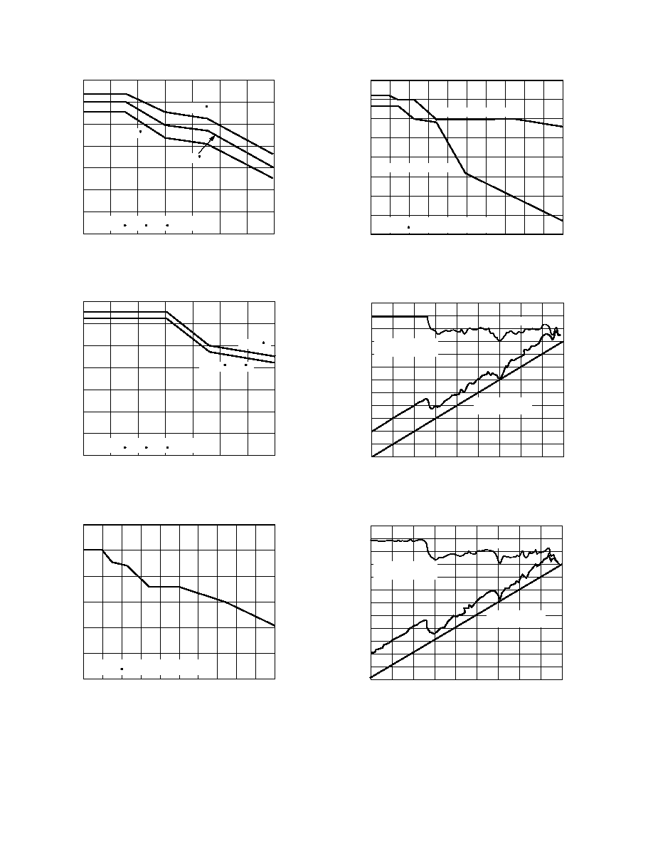
REV. 0
AD6645
10
FREQUENCY MHz
SNR dB
0
10
20
30
40
50
60
70
ENCODE = 80MSPS @ AIN = 1dBFS
TEMP = 40 C, +25 C, +85 C
72.0
72.5
73.0
73.5
74.0
74.5
75.0
75.5
T = +25 C
T = +85 C
T = 40 C
TPC 7. Noise vs. Analog Frequency
ANALOG INPUT FREQUENCY MHz
WORST CASE HARMONIC dBc
0
10
20
30
40
50
60
70
ENCODE = 80MSPS @ AIN = 1dBFS
TEMP = 40 C, +25 C, +85 C
80
82
84
86
88
90
92
94
T = +25 C
T = 40 C, +85 C
TPC 8. Harmonics vs. Analog Frequency
ANALOG FREQUENCY MHz
SNR dB
0
20
80
40
100
60
ENCODE = 80MSPS @ AIN = 1dBFS
TEMP = 25 C
70
71
72
73
74
75
76
120
140
160
180
200
TPC 9. Noise vs. Analog Frequency (IF)
ANALOG FREQUENCY MHz
HARMONICS dBc
0
20
80
40
100
60
ENCODE = 80MSPS @ AIN = 1dBFS
TEMP = 25 C
60
65
120
140
160
180
200
70
80
90
100
75
85
95
WORST OTHER SPUR
HARMONICS (2ND, 3RD)
TPC 10. Harmonics vs. Analog Frequency (IF)
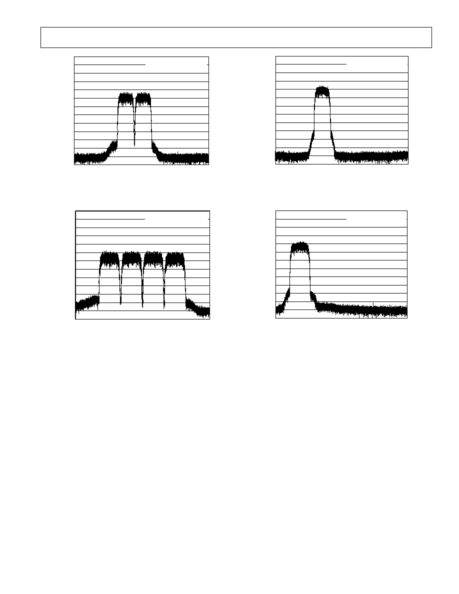
ANALOG INPUT POWER LEVEL dBFS
WORST CASE SPURIOUS dBFS AND dBc
0
90
10
20
30
40
50
60
70
80
90
100
110
80
70
60
50
40
30
20
ENCODE = 80MSPS
AIN = 30.5MHz
dBc
SFDR = 90dB
REFERENCE LINE
120
dBFS
10
0
TPC 11. Single Tone SFDR @ 30.5 MHz
ANALOG INPUT POWER LEVEL dBFS
WORST CASE SPURIOUS dBFS AND dBc
0
90
10
20
30
40
50
60
70
80
90
100
110
80
70
60
50
40
30
20
ENCODE = 80MSPS
AIN = 69.1MHz
dBc
SFDR = 90dB
REFERENCE LINE
120
dBFS
10
0
TPC 12. Single Tone SFDR @ 69.1 MHz
REV. 0
11
AD6645
ENCODE = 80MSPS
AIN = 30.5MHz,
31.5MHz (7dBFS)
NO DITHER
FREQUENCY MHz
130
0
5
10
15
20
25
30
35
40
120
110
100
90
80
70
60
50
40
30
20
10
0
dBFS
2
F
1
+
F
2
F
1
+
F
2
F
2
F
1
2
F
2
+
F
1
2
F
1
F
2
2
F
2
F
1
TPC 13. Two Tones @ 30.5 MHz and 31.5 MHz
INPUT POWER LEVEL F1 = F2 dBFS
WORST CASE SPURIOUS dBFS AND dBc
0
77
10
20
30
40
50
60
70
80
90
100
110
67
57
47
37
27
17
7
ENCODE = 80MSPS
F1 = 30.5MHz
F2 = 31.5MHz
dBc
dBFS
SFDR = 90dB
REFERENCE LINE
TPC 14. Two Tone SFDR @ 30.5 MHz and 31.5 MHz
ENCODE FREQUENCY MHz
SNR, WORST CASE SPURIOUS dB
AND dBc
15
65
70
80
90
30
45
60
75
90
105
WORST SPUR @ AIN = 2.2MHz
SNR @ AIN = 2.2MHz
75
85
95
100
TPC 15. SNR, Worst Spurious vs. Encode @ 2.2 MHz
2
F
2
F
1
ENCODE = 80MSPS
AIN = 55.25MHz,
56.25MHz (7dBFS)
NO DITHER
FREQUENCY MHz
130
0
5
10
15
20
25
30
35
40
120
110
100
90
80
70
60
50
40
30
20
10
0
dBFS
2
F
1
+
F
2
F
1
+
F
2
F
2
F
1
2
F
2
+
F
1
2
F
1
F
2
TPC 16. Two Tone SFDR @ 55.25 MHz and 56.25 MHz
77
67
57
47
37
27
17
7
INPUT POWER LEVEL F1 = F2 dBFS
WORST CASE SPURIOUS dBFS AND dBc
0
10
20
30
40
50
60
70
80
90
100
110
ENCODE = 80MSPS
F1 = 55.25MHz
F2 = 56.25MHz
dBc
dBFS
SFDR = 90dB
REFERENCE LINE
TPC 17. Two Tone SFDR @ 55.25 MHz and 56.25 MHz
ENCODE FREQUENCY MHz
SNR, WORST CASE SPURIOUS dB
AND dBc
15
65
70
80
90
30
45
60
75
90
105
WORST SPUR @ AIN = 69.1MHz
SNR @ AIN = 69.1MHz
75
85
95
TPC 18. SNR, Worst Spurious vs. Encode @ 69.1 MHz
REV. 0
AD6645
12
FREQUENCY MHz
0
130
120
110
100
90
80
70
60
50
40
30
20
10
0
5
10
15
20
25
30
35
40
5
3
2
6
4
dBFS
ENCODE = 80.0MSPS
AIN = 30.5MHz @ 29.5 dBFS
NO DITHER
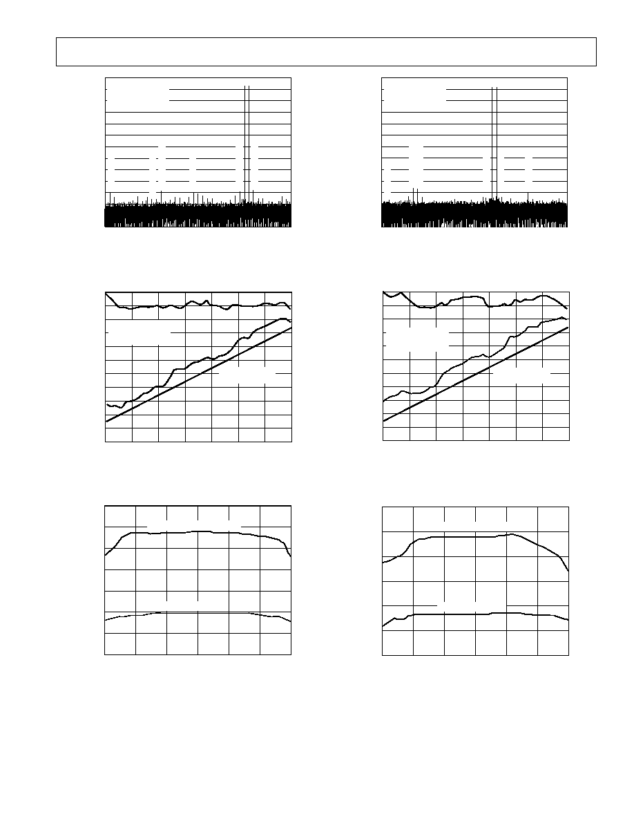
TPC 19. 1 M FFT without Dither
ANALOG INPUT LEVEL
90
0
10
20
30
40
50
60
70
80
90
100
110
80
70
60
50
40
30
20
10
0
dBFS
ENCODE = 80.0MSPS
AIN = 30.5MHz
NO DITHER
SFDR = 90 dB
REFERENCE LINE
WORST-CASE SPURIOUS dBc
TPC 20. SFDR without Dither
FREQUENCY MHz
130
0
5
10
15
20
25
30
35
40
120
110
100
90
80
70
60
50
40
30
20
10
0
dBFS
2
6
5
4
3
ENCODE = 76.8MSPS
AIN = 69.1MHz @
1dBFS
SNR = 73.5dB
SFDR = 89.0dBc
TPC 21. Single Tone 69.1 MHz: Encode = 76.8 MSPS
FREQUENCY MHz
130
0
5
10
15
20
25
30
35
40
120
110
100
90
80
70
60
50
40
30
20
10
0
5
3
2
6
4
dBFS
ENCODE = 80.0MSPS
AIN = 30.5MHz @ 29.5dBFS
WITH DITHER @ 19.2 dBm
TPC 22. 1 M FFT with Dither
ANALOG INPUT LEVEL
90
0
10
20
30
40
50
60
70
80
90
100
110
80
70
60
50
40
30
20
10
0
dBFS
ENCODE = 80.0MSPS
AIN = 30.5MHz
WITH DITHER @ 19.2 dBm
SFDR = 90 dB
REFERENCE LINE
SFDR = 100 dB
REFERENCE LINE
WORST-CASE SPURIOUS dBc
TPC 23. SFDR with Dither
FREQUENCY MHz
130
0
5
10
15
20
25
30
35
40
120
110
100
90
80
70
60
50
40
30
20
10
0
dBFS
2
6
5
4
3
ENCODE = 76.8MSPS
AIN = WCDMA @ 69.1MHz
TPC 24. WCDMA Tone 69.1 MHz: Encode = 76.8 MSPS
REV. 0
13
AD6645
FREQUENCY MHz
130
0
5
10
15
20
25
30
35
40
120
110
100
90
80
70
60
50
40
30
20
10
0
dBFS
ENCODE = 76.8MSPS
AIN = 2WCDMA @ 59.6MHz
TPC 25. 2 WCDMA Carriers @ A
IN
= 59.6 MHz:
Encode = 76.8 MSPS
FREQUENCY MHz
0
2.5
5.0
7.5 10.0 12.5 15.0 17.5 20.0 22.5 25.0 27.5 30.0
130
120
110
100
90
80
70
60
50
40
30
20
10
0
ENCODE = 61.44MSPS
AIN = 4WCDMA @ 46.08MHz
dBFS
TPC 26. 4 WCDMA Carriers @ A
IN
= 46.08 MHz:
Encode = 61.44 MSPS
6
5
4
2
3
FREQUENCY MHz
130
0
120
110
100
90
80
70
60
50
40
30
20
10
0
5
10
15
20
25
30
35
40
ENCODE = 76.8MSPS
AIN = WCDMA @ 140MHz
dBFS
TPC 27. WCDMA Tone 140 MHz: Encode = 76.8 MSPS
130
120
110
100
90
80
70
60
50
40
30
20
10
0
2
3
6
4
5
ENCODE = 61.44MSPS
AIN = WCDMA @ 190MHz
dBFS
FREQUENCY MHz
0
2.5
5.0
7.5 10.0 12.5 15.0 17.5 20.0 22.5 25.0 27.5 30.0
TPC 28. WCDMA Tone 190 MHz: Encode = 61.44 MSPS
REV. 0
AD6645
14
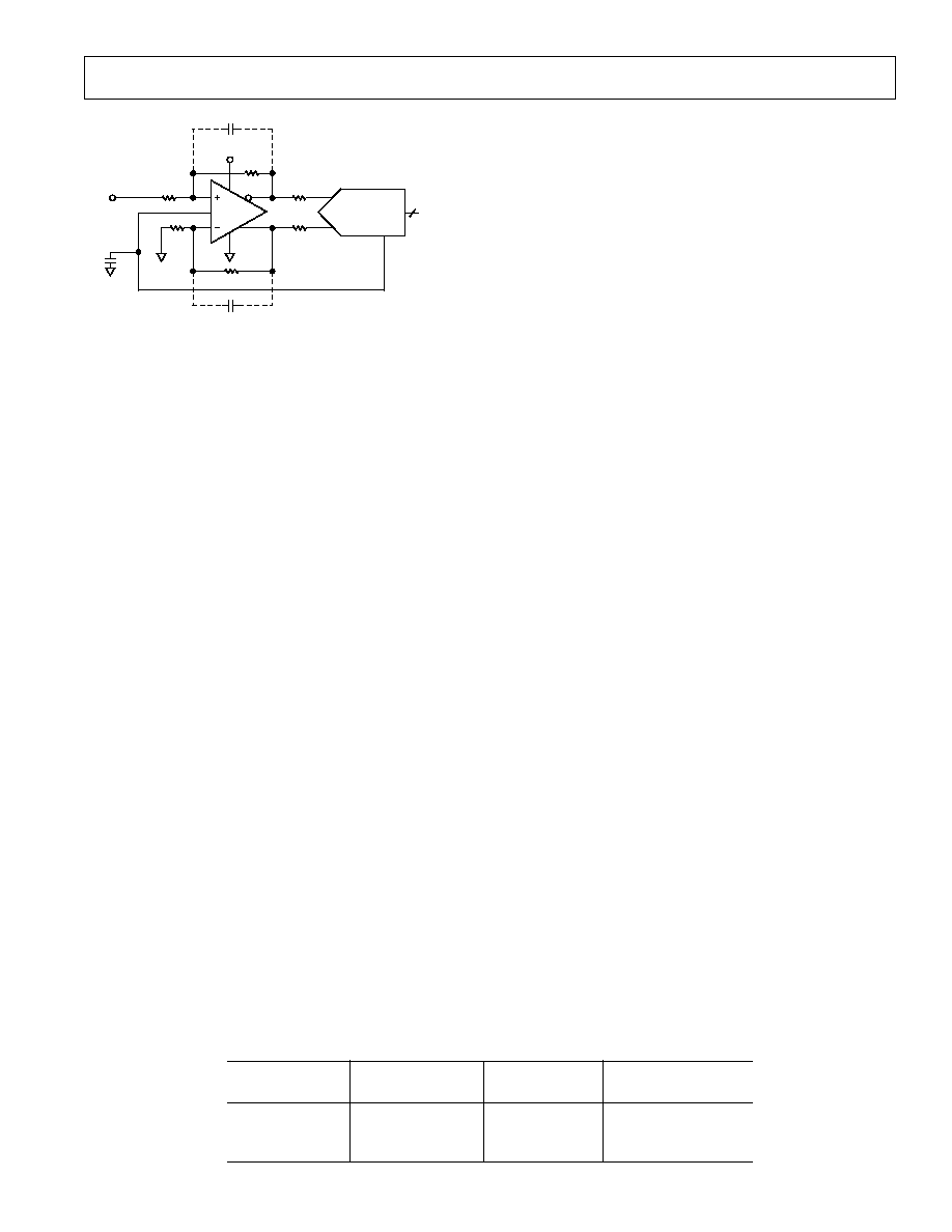
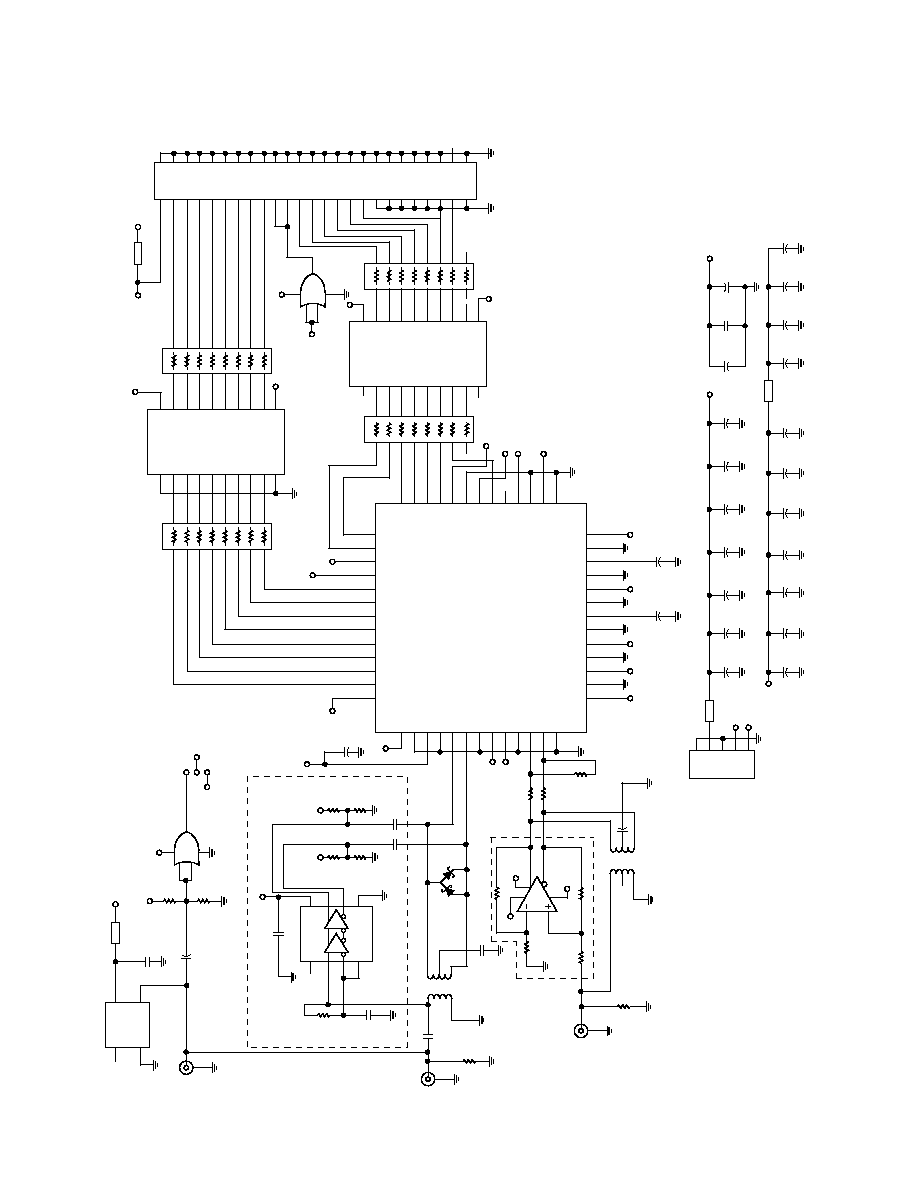
THEORY OF OPERATION
The AD6645 analog-to-digital converter (ADC) employs a three
stage subrange architecture. This design approach achieves the
required accuracy and speed while maintaining low power and
small die size.
As shown in the functional block diagram, the AD6645 has
complementary analog input pins, AIN and
AIN. Each analog
input is centered at 2.4 V and should swing
±0.55 V around this
reference (see Figure 2). Since AIN and
AIN are 180 degrees out
of phase, the differential analog input signal is 2.2 V
peak-to-peak.
Both analog inputs are buffered prior to the first track-and-hold,
TH1. The high state of the ENCODE pulse places TH1 in hold
mode. The held value of TH1 is applied to the input of a 5-bit
coarse ADC1. The digital output of ADC1 drives a 5-bit digital-
to-analog converter, DAC1. DAC1 requires 14 bits of precision,
which is achieved through laser trimming. The output of DAC1
is subtracted from the delayed analog signal at the input of TH3
to generate a first residue signal. TH2 provides an analog pipe-
line delay to compensate for the digital delay of ADC1.
The first residue signal is applied to a second conversion stage
consisting of a 5-bit ADC2, 5-bit DAC2, and pipeline TH4.
The second DAC requires 10 bits of precision, which is met
by the process with no trim. The input to TH5 is a second resi-
due signal generated by subtracting the quantized output of
DAC2 from the first residue signal held by TH4. TH5 drives
a final 6-bit ADC3.
The digital outputs from ADC1, ADC2, and ADC3 are added
together and corrected in the digital error correction logic to
generate the final output data. The result is a 14-bit parallel
digital CMOS-compatible word, coded as two's complement.
APPLYING THE AD6645
Encoding the AD6645
The AD6645 encode signal must be a high quality, extremely
low phase noise source to prevent degradation of performance.
Maintaining 14-bit accuracy places a premium on encode clock
phase noise. SNR performance can easily degrade by 34 dB
with 70 MHz analog input signals when using a high jitter clock
source. See AN-501, "Aperture Uncertainty and ADC System
Performance" for complete details.
For optimum performance, the AD6645 must be clocked differ-
entially. The encode signal is usually ac-coupled into the ENC
and
ENC pins via a transformer or capacitors. These pins are
biased internally and require no additional bias.
Shown below is one preferred method for clocking the AD6645.
The clock source (low jitter) is converted from single-ended to
differential using a RF transformer. The back-to-back Schottky
diodes across the transformer secondary limit clock excursions
into the AD6645 to approximately 0.8 V p-p differential. This
helps prevent the large voltage swings of the clock from feeding
through to other portions of the AD6645, and limits the noise
presented to the encode inputs.
ENCODE
ENCODE
0.1 F
T1-4T
HSMS2812
DIODES
AD6645
CLOCK
SOURCE
Figure 8. Crystal Clock Oscillator, Differential Encode
If a low jitter clock is available, another option is to ac-couple a
differential ECL/PECL signal to the encode input pins as shown
below. The MC100EL16 (or same family) from ON-SEMI
offers excellent jitter performance.
ENCODE
ENCODE
AD6645
VT
VT
0.1 F
0.1 F
ECL/
PECL
Figure 9. Differential ECL for Encode
Driving the Analog Inputs
As with most new high-speed, high dynamic range analog-to-
digital converters, the analog input to the AD6645 is differential.
Differential inputs improve on-chip performance as signals are
processed through attenuation and gain stages. Most of the
improvement is a result of differential analog stages having high
rejection of even-order harmonics. There are also benefits at the
PCB level. First, differential inputs have high common-mode
rejection to stray signals such as ground and power noise. Sec-
ond, they provide good rejection to common-mode signals such
as local oscillator feed-through.
The AD6645 analog input voltage range is offset from ground by
2.4 V. Each analog input connects through a 500
W resistor to the
2.4 V bias voltage and to the input of a differential buffer (Fig-
ure 2). The resistor network on the input properly biases the
followers for maximum linearity and range. Therefore, the analog
source driving the AD6645 should be ac-coupled to the input
pins. Since the differential input impedance of the AD6645 is 1 k
W,
the analog input power requirement is only 2 dBm, simplifying
the driver amplifier in many cases. To take full advantage of this
high input impedance, a 20:1 transformer would be required.
This is a large ratio and could result in unsatisfactory perfor-
mance. In this case, a lower step-up ratio could be used. The
recommended method for driving the analog input of the
AD6645 is to use a 4:1 RF transformer. For example, if RT
were set to 60.4
W and RS were set to 25 W, along with a 4:1
impedance ratio transformer, the input would match to a 50
W
source with a full-scale drive of 4.8 dBm. Series resistors (RS)
on the secondary side of the transformer should be used to
isolate the transformer from A/D. This will limit the amount of
dynamic current from the A/D flowing back into the secondary
of the transformer. The 50
W impedance matching can also be
incorporated on the secondary side of the transformer as shown
in the evaluation board schematic (Figure 13).
AIN
AIN
ADT4-1WT
AD6645
ANALOG INPUT
SIGNAL
0.1 F
R
T
R
S
R
S
Figure 10. Transformer-Coupled Analog Input Circuit
In applications where dc-coupling is required, a differential
output op amp such as the AD8138 from Analog Devices can
be used to drive the AD6645 (Figure 11). The AD8138 op amp
provides single-ended-to-differential conversion, which reduces
overall system cost and minimizes layout requirements.
REV. 0
15
AD6645
AD6645
AIN
AIN
V
REF
AD8138
V
OCM
5V
499
499
499
499
25
25
C
F
V
IN
C
F
DIGITAL
OUTPUTS
Figure 11. DC-Coupled Analog Input Circuit
Power Supplies
Care should be taken when selecting a power source. The use of
linear dc supplies with rise-times of <45 ms is highly recom-
mended. Switching supplies tend to have radiated components
that may be "received" by the AD6645. Each of the power
supply pins should be decoupled as closely to the package as
possible using 0.1
mF chip capacitors.
The AD6645 has separate digital and analog power supply pins.
The analog supplies are denoted AV
CC
and the digital supply
pins are denoted DV
CC
. Although analog and digital supplies
may be tied together, best performance is achieved when the
supplies are separate. This is because the fast digital output
swings can couple switching current back into the analog supplies.
Note that AV
CC
must be held within 5% of 5 V. The AD6645 is
specified for DV
CC
= 3.3 V as this is a common supply for
digital ASICS.
Digital Outputs
Care must be taken when designing the data receivers for the AD6645.
It is recommended that the digital outputs drive a series resistor
followed by a gate such as the 74LCX574. To minimize capaci-
tive loading, there should only be one gate on each output pin.
An example of this is shown in the evaluation board schematic
shown in Figure 13. The digital outputs of the AD6645 have a
constant output slew rate of 1 V/ns. A typical CMOS gate combined
with a PCB trace will have a load of approximately 10 pF. There-
fore, as each bit switches 10 mA
10
1
1
pF
V
ns
¥
(
)
of
dynamic current per bit will flow in or out of the device. A full-
scale transition can cause up to 140 mA (14 bits
¥ 10 mA/bit) of
current to flow through the output stages. The series resistors
should be placed as close to the AD6645 as possible to limit the
amount of current that can flow into the output stage. These
switching currents are confined between ground and the DV
CC
pin. Standard TTL gates should be avoided since they can appre-
ciably add to the dynamic switching currents of the AD6645. It
should be noted that extra capacitive loading will increase out-
put timing and invalidate timing specifications. Digital output
timing is guaranteed for output loads up to 10 pF.
Digital output states for given analog input levels are shown in Table I.
Grounding
For optimum performance, it is highly recommended that a com-
mon ground be utilized between the analog and digital power
planes. The primary concern with splitting grounds is that dynamic
currents may be forced to travel significant distances in the sys-
tem before recombining back at the common source ground. This
can result in a large and undesirable ground loop. The most
common place for this to occur is on the digital outputs of the
ADC. Ground loops can contribute to digital noise being coupled
back onto the ADC front end. This can manifest itself as either
harmonic spurs, or very high order spurious products that can
cause excessive spikes on the noise floor. This noise coupling is
less likely to occur at lower clock speeds since the digital noise has
more time to settle between samples. In general, splitting the
analog and digital grounds can frequently contribute to undesir-
able EMI-RFI and should therefore be avoided.
Conversely, if not properly implemented, common grounding can
actually impose additional noise issues since the digital ground
currents are riding on top of the analog ground currents in close
proximity to the ADC input. To minimize the potential for
noise coupling further, it is highly recommended that multiple
ground return traces/vias be placed such that the digital output
currents do not flow back towards the analog front end, but are
routed quickly away from the ADC. This does not require a
split in the ground plane and can be accomplished by simply
placing substantial ground connections directly back to the
supply at a point between the analog front end and the digital
outputs. The judicious use of ceramic chip capacitors between
the power supply and ground planes will also help suppress
digital noise. The layout should incorporate enough bulk capacitance
to supply the peak current requirements during switching periods.
Layout Information
The schematic of the evaluation board (Figure 13) represents a
typical implementation of the AD6645. A multilayer board is
recommended to achieve best results. It is highly recommended
that high quality, ceramic chip capacitors be used to decouple
each supply pin to ground directly at the device. The pinout of
the AD6645 facilitates ease of use in the implementation of
high-frequency, high-resolution design practices. All of the digital
outputs are segregated to two sides of the chip, with the inputs on
the opposite side for isolation purposes.
Care should be taken when routing the digital output traces. To
prevent coupling through the digital outputs into the analog
portion of the AD6645, minimal capacitive loading should be
placed on these outputs. It is recommended that a fan-out of
only one gate should be used for all AD6645 digital outputs.
The layout of the encode circuit is equally critical. Any noise
received on this circuitry will result in corruption in the digitiza-
tion process and lower overall performance. The encode clock
must be isolated from the digital outputs and the analog inputs.
Table I. Two's Complement Output Coding
AIN
AIN
Output
Output
Level
Level
State
Code
V
REF
+ 0.55 V
V
REF
0.55 V
Positive FS
01 1111 1111 1111
V
REF
V
REF
Midscale
00...0/11...1
V
REF
0.55 V
V
REF
+ 0.55 V
Negative FS
10 0000 0000 0000
REV. 0
AD6645
16
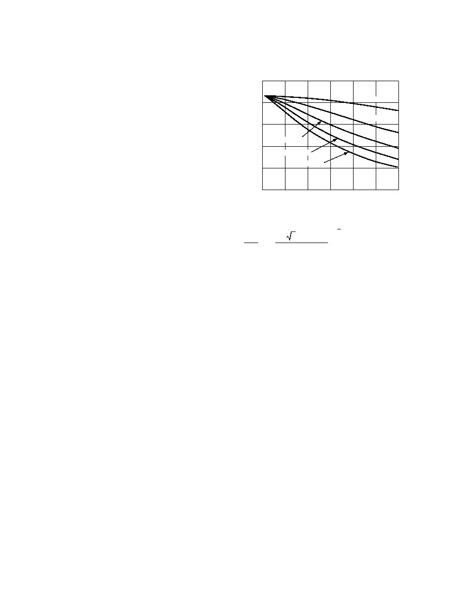
Jitter Considerations
The signal-to-noise ratio (SNR) for an ADC can be predicted.
When normalized to ADC codes, the above equation accurately
predicts the SNR based on three terms. These are jitter, average
DNL error, and thermal noise. Each of these terms contributes
to the noise within the converter.
F
ANALOG
= analog input frequency
t
j rms
= rms jitter of the encode (rms sum of encode source and
internal encode circuitry)
= average DNL of the ADC (typically 0.41 LSB)
n = number of bits in the ADC
V
NOISE rms
= V rms thermal noise referred to the analog input of
the ADC (typically 0.9 LSB rms)
For a 14-bit analog-to-digital converter, like the AD6645, aperture
jitter can greatly affect the SNR performance as the analog
frequency is increased. The chart below shows a family of curves
that demonstrate the expected SNR performance of the AD6645 as
jitter increases. The chart is derived from the above equation.
For a complete discussion of aperture jitter, please consult
AN-501, "Aperture Uncertainty and ADC System Performance."
JITTER ps
55
0
0.1
SNR dBFS
60
65
70
75
80
0.2
0.3
0.4
0.5
0.6
AIN = 110MHz
AIN = 150MHz
AIN = 190MHz
AIN = 30MHz
AIN = 70MHz
Figure 12. Jitter vs. SNR
SNR
F
t
V
j rms
n
N
n
=
-
¥
¥
(
)
+ +
Ê
Ë
Á
^
¯
~ + ¥ ¥
Ê
Ë
Á
^
¯
~
È
Î
Í
Í
ù
û
ú
ú
1 76 20
2
1
2
2
2
2
2
2
2
1
2
.
log
p
e
ANALOG
OISE rms

REV. 0
17
AD6645
Table II. AD6645ASQ/PCB Bill of Materials
Item
No.
Qty
Reference ID
1
Description
Manufacturer
1
1
6645EE01C
AD6644/AD6645 Evaluation Printed Circuit Board
PCSM, Inc. (6645EE01C)
2
3
C1, C2, C38
Capacitor, Tantalum SMT T491C, 10
mF; 16 V; 10%
Kemet (T491C106M016AS)
3
9
C3, C7C11, C16,
Capacitor, SMT 0508, 0.1
mF; 16 V; 10%
Presidio Components
C30, C32
(0508X7R104K16VP6)
4
8
C4, C22C26, C29,
Capacitor, SMT 0805, 0.1
mF; 25 V; 10%
Panasonic (ECJ-2VB1E104K)
(C33), (C34), C39
5
0
(C5, C6)
Capacitor, SMT 0805, 0.01
mF; 50 V; 10%
Panasonic (ECJ-2YB1H103K)
6
9
C12C14, C17C21,
Capacitor, SMT 0508, 0.01
mF; 16 V; 10%
Presidio Components
C40
(0508X7R103M2P3)
7
1
CR1
Diode, Schottky Barrier, Dual
Panasonic (MA716-TX)
8
1
E3, E4, E5
100" Straight Male Header (Single Row), 3 of 50 pins
Samtec (TSW-1-50-08-G-S)
9
4
F1F4
EMI Suppression Ferrite Chip, SMT 0805
Steward (HZ0805E601R-00)
10
1
J1
Connector, PCB Pin Strip; 5 pins; 5 mm pitch
Wieland (Z5.530.0525.0)
11
1
J1
Connector, PCB Terminal; 5 pins; 5 mm pitch
Wieland (25.602.2553.0)
12
1
J2
Terminal Strip, 50 pin; right angle
Samtec (TSW-125-08-T-DRA)
13
0
(J3)
Connector, SMA; RF; Gold
Johnson Components, Inc.
(142-0701-201)
14
2
J4, J5
Connector, Coaxial RF Receptacle; 50
W
AMP (227699-2)
15
0
(R1)
Resistor, SMT 0402; 100; 1/16w; 1%
Panasonic (ERJ-2RKF1000X)
16
0
(R2)
2
Resistor, SMT 1206; 60.4; 1/8w; 1%
Panasonic (ERJ-8ENF60R4V)
17
0
(R3, R4, R5, R8)
Resistor, SMT 0805; 499; 1/10w; 1%
Panasonic (ERJ-6ENF4990V)
18
2
R6, R7
Resistor, SMT 0805; 25.5; 1/10w; 1%
Panasonic (ERJ-6ENF25R5V)
19
1
R9
Resistor, SMT 0805; 348; 1/10w; 1%
Panasonic (ERJ-6ENF3480V)
20
1
R10
Resistor, SMT 0805; 619; 1/10w; 1%
Panasonic (ERJ-6ENF6190V)
21
0
(R11), (R13)
Resistor, SMT 0805; 66.5; 1/10w; 1%
Panasonic (ERJ-6ENF66R5V)
22
0
(R12), (R14)
Resistor, SMT 0805; 100; 1/10w; 1%
Panasonic (ERJ-6ENF1000V)
23
1
R15
2
Resistor, SMT 0402; 178; 1/16w; 1%
Panasonic (ERJ-2RKF1780X)
24
1
R35
Resistor, SMT 0805; 49.9; 1/10w; 1%
Panasonic (ERJ-6ENF49R9V)
25
2
RN1, RN3
Resistor Array, SMT 0402; 470; 1/4w; 5%
Panasonic (EXB2HV471JV)
26
2
RN2, RN4
Resistor Array, SMT 0402; 220; 1/4w; 5%
Panasonic (EXB2HV221JV)
27
1
T2
RF Transformer, SMT KK81, 0.2350 MHz; 4:1
W Ratio Mini-Circuits (T4-1-KK81)
28
1
T3
RF Transformer, SMT CD542, 2775 MHz; 4:1
W Ratio Mini-Circuits (ADT4-1WT)
29
1
U1
I.C., QFP-52; 14-Bit, 80 MSPS
Analog Devices (AD6645ASQ)
Wideband Analog-to-Digital Converter
30
2
U2, U7
I.C., SOIC-20; Octal D-Type Flip-Flop
Fairchild (74LCX574WM)
31
0
(U3)
I.C., SOIC-8; Low Distortion Differential ADC Driver
Analog Devices (AD8138AR)
32
2
U4, U6
I.C., SMT SOT-23; TinyLogic UHS 2-Input OR Gate
Fairchild (NC7SZ32)
33
1
U5
3
Clock Oscillator, Full Size MX045; 80 MHz
CTS Reeves (MXO45-80)
34
4
U5
3
Connector, Miniature Spring Socket,
Amp (5-330808-3)
35
0
(U8)
I.C., SOIC-8; Differential Receiver
Motorola (MC100EL16)
36
4
See drawing
Circuit Board Support on Base
Richo (CBSB-14-01)
37
1
See drawing
0.100" Shorting Block
Jameco (152670)
NOTES
1
Reference designators in parentheses are not installed on standard units. (AC-coupled AIN and ENCODE.)
AC-coupled AIN is standard, R3, R4, R5, R8, and U3 are not installed.
If dc-coupled AIN is required, C30, T3, and R15 are not installed.
AC-coupled ENCODE is standard. C5, C6, C33, C34, R1, R11R14, and U8 are not installed.
If PECL ENCODE is required, CR1 and T2 are not installed.
2
R2 is installed for 50
W impedance input matching on the primary of T3. R15 is not installed.
R15 is installed for 50
W impedance input matching on the secondary of T3. R2 is not installed.
3
U5 Clock Oscillator is installed with pin sockets for removal if OPT_CLK input is used.
REV. 0
AD6645
18
1
2
3
4
5
1
2
3
4
5
6
7
8
9
10
11
13
14
15
16
17
18
19
20
21
22
23
24
25
26
27
28
29
30
31
32
33
34
35
36
37
38
39
40
12
41
42
43
44
45
46
47
48
49
50
51
52
1
2
3
4
5
6
7
8
9
10
11
12
13
14
15
16
RN3
(SEE NOTE 4)
1
2
3
4
5
6
7
8
9
10
11
12
13
14
15
16
1
2
3
4
5
6
7
8
9
10
11
12
13
14
15
16
17
18
19
20
U2
GND
CLOCK
OUT
EN
D0
D1
D2
D3
D4
D5
D6
D7
VCC
Q0
Q1
Q2
Q3
Q4
Q5
Q6
Q7
1
2
3
4
5
6
7
8
9
10
11
12
13
14
15
16
17
18
19
20
U7
GND
CLOCK
OUT_EN
D0
D1
D2
D3
D4
D5
D6
D7
VCC
Q0
Q1
Q2
Q3
Q4
Q5
Q6
Q7
1
2
3
4
5
6
7
8
9
10
11
12
13
14
15
16
RN1
(SEE NOTE 4)
1
2
3
4
5
6
7
8
9
10
11
12
13
14
15
16
1
2
3
4
5
7
9
11
13
15
17
19
21
23
25
27
29
31
33
35
37
39
41
43
45
47
49
6
8
10
12
14
16
18
20
22
24
26
28
30
32
34
36
38
40
42
44
46
48
50
R2 IS INSTALLED FOR INPUT MATCHING ON THE PRIMARY OF T3. R15 IS NOT INSTALLED.
R15 IS INSTALLED FOR INPUT MATCHING ON THE SECONDARY OF T3.
R2 IS NOT INSTALLED.
AC-COUPLED AIN IS STANDARD. R3, R4, R5, R8, AND U3 ARE NOT INSTALLED.
IF DC-COUPLED AIN IS REQUIRED, C30, R15, AND T3 ARE NOT INSTALLED.
AC-COUPLED ENCODE IS STANDARD. C5, C6, C33, C34, R1, R11R14 AND U8 ARE NOT INSTALLED.
IF PECL ENCODE IS REQUIRED, CR1, AND T3 ARE NOT INSTALLED.
IF AD6644 IS USED: VALUE FOR RN1RN4 IS 100 OHM.
IF AD6645 IS USED: VALUE FOR RN1RN3 IS 470 OHM, VALUE FOR RN2 AND RN4 IS 220 OHM.
NOTES
1.
2.
3.
4.
AD6644
/
AD6645
GND
VREF
GND
ENC
ENC
GND
AVCC
AVCC
GND
AIN
AIN
GND
DVCC
AVCC
GND
GND
GND
C1
C2
AVCC
AVCC
GND
AVCC
GND
GND
AVCC
D3
D2
D1
D0
DMID
GND
DVCC
OVR
AVCC
DNC
GND
AVCC
GND
DRY
D13
D12
D11
D10
D9
D8
D7
D6
DVCC
GND
D5
D4
DC-COUPLED AIN OPTION
2
1
2
1
2
3
4
5
GND
BUFLAT
U6
BUFLAT
FERRITE
12
F2
+
3P3VIN
+
3P3V
J2
+3
P3VD
1
2
3
4
1
2
J1
+3
P
3
VIN
5V
5
F1
C2
10
F
C16
0.1
F
C17
0.01
F
C18
0.01
F
C19
0.01
F
C20
0.01
F
C21
0.01
F
C40
0.01
F
C39
0.1
F
C38
10
F
12
+
3P3V
C1
10
F
C9
0.1
F
C10
0.1
F
C11
0.01
F
C12
0.01
F
C13
0.01
F
C14
0.01
F
C23
0.1
F
C24
0.1
F
C25
0.1
F
C26
0.1
F
+5VA
+5VA
+5VA
+5VA
+5VA
C8
0.1
F
C7
0.1
F
+5VA
+5VA
+3
P3V
PREF
GND
+
3P3V
DR_OUT
+3
P3V
C32
0.1
F
VREF
+5VA
+5VA
RN4
(SEE NOTE 4)
R7
25
R6
25
R15
1
176.4
1
2
3
6
5
4
T3
IMPEDANCE
RATIO
ADT4-1WT 4:1
C30
0.1
F
R2
1
60.4
1
2
J5
AIN
1
8
3
2
6
4
5
AD8138
R4 499
VREF
5V
U3
+5VA
R5 499
R3
499
R5
499
C29
0.1
F
T2
IMPEDANCE
RATIO
1:4
3
2
1
4
61
2
3
CR1
C4
0.1
F
1
2
ENC
J4
R35
49.9
R13
66.5
R14
100
C34
0.1
F
C33
0.1
F
R11
66.5
R12
100
+5VA
+5VA
1
2
3
4
8
7
6
5
NC
VBB
VCC
VEE
U8
+5VA
C6
0.01
F
R1
100
C5
.01
F
PECL ENCODE OPTION
3
GND
FERRITE
+5VA
C22
0.1
F
VCC
OUT
NC
GND
U5
C3
0.1
F
E3
E5
E4
BUFLAT
DR_OUT
+3
P3VD
U4
R10
619
R9
348
11
4
78
K1115
66.66MHz (AD6644
)
80MHz (AD6645
)
OPT_CLK
J3
BUFLAT
NC7SZ32
BNC
BNC
+
3P3VD
+3
P3VD
NC7SZ32
MC100EL16
74LCX574
FERRITE
FERRITE
+5VA
5V
+
+
SMA
+3
P
3
V
OPT_LAT
V1
R8
Q
Q
D
D
OPTIONAL
HSMS2812
HEADER 50
74LCX574
B06
B07
B08
B09
B10
B11
B12
B13
B00
B01
B02
B03
B04
B05
OVR
+3
P3VD
F3
F4
RN2
(SEE NOTE 4)
Figure 13. Evaluation Board Schematic
REV. 0
19
AD6645
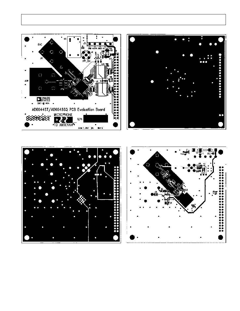
Figure 14. Top Signal Level
Figure 15. 5.0 V/3.3 V Plane Layers 3 and 4
Figure 16. Ground Plane Layer 2 and 5
Figure 17. Bottom Signal Layer
REV. 0
20
C0264702/02(0)
PRINTED IN U.S.A.
AD6645
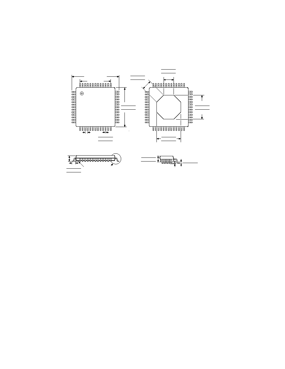
OUTLINE DIMENSIONS
Dimensions shown in millimeters and (inches).
52-Lead PowerQuad 4 (LQFP_ED)
(SQ-52)
0.65 (0.026)
0.38 (0.015)
0.32 (0.013)
0.22 (0.009)
12.00 (0.472) SQ
10.20 (0.402)
10.00 (0.394) SQ
9.80 (0.386)
TOP VIEW
(PINS DOWN)
40
52
1
14
13
26
27
39
7.80 (0.307)
1.60
(0.063)
MAX
VIEW A
SEATING
PLANE
0.75 (0.030)
0.60 (0.024)
0.45 (0.018)
0.15 (0.006)
0.05 (0.002)
VIEW A
0.10 (0.004)
COPLANARITY
1.45 (0.057)
1.40 (0.055)
1.35 (0.053)
40
52
1
14
13
26
27
39
EXPOSED
HEATSINK
(CENTERED)
2.35 (0.093)
2.20 (0.087)
2.05 (0.081)
(4 PLCS)
6.00 (0.236)
5.90 (0.232)
5.80 (0.228)
6.00 (0.236)
5.90 (0.232)
5.80 (0.228)
2.65 (0.104)
2.50 (0.098)
2.35 (0.093)
(4 PLCS)
BOTTOM VIEW
(PINS UP)
CONTROLLING DIMENSIONS ARE IN MILLIMETERS; INCH DIMENSIONS (IN PARENTHESES) ARE ROUNDED-OFF MILLIMETER
EQUIVALENTS FOR REFERENCE ONLY AND ARE NOT APPROPRIATE FOR USE IN DESIGN.
THE AD6645 POWERQUAD 4 (LQFP_ED) HAS A THERMALLY AND ELECTRICALLY CONDUCTIVE HEAT SLUG EXPOSED ON THE
BOTTOM OF THE PACKAGE WHICH CAN BE UTILIZED FOR ENHANCED THERMAL MANAGEMENT. IT IS RECOMMENDED THAT
NO UNMASKED ACTIVE PCB TRACES OR VIAS BE LOCATED UNDER THE PACKAGE THAT COULD COME INTO CONTACT WITH
THE GROUNDED HEAT SLUG. ALTHOUGH NOT A REQUIREMENT FOR SPECIFIED OPERATION, SOLDERING THE SLUG TO A
GROUND PLANE WITH SUFFICIENT THERMAL CAPACITY WILL REDUCE THE JUNCTION TEMPERATURE OF THE DEVICE. THIS
MAY PROVE BENEFICIAL IN HIGH RELIABILITY APPLICATIONS WHERE LOWER JUNCTION TEMPERATURES TYPICALLY CONTRIBUTE
TO INCREASED SEMICONDUCTOR RELIABILITY.
Document Outline
- Specifications
- Package Drawings
- Ordering Guide
- Features
- Applications
- Absolute Maximum Ratings
- Functional Block Diagram
- Pin Function Description
- Circuit Description
- PRODUCT HIGHLIGHTS
- PRODUCT DESCRIPTION
- THERMAL CHARACTERISTICS EXPLANATION OF TEST LEVELS
- CAUTION
- Pinout
- EQUIVALENT CIRCUITS
- THEORY OF OPERATION
- APPLYING THE AD6645
- DIAGRAMS
- Timing Diagram
- Analog Input Stage
- Encode Inputs
- Compensation Pin, C1 or C2
- Digital Output Stage
- 2.4 V Reference
- DMID Reference
- Differential ECL for Encode
- Transformer-Coupled Analog Input Circuit
- Crystal Clock Oscillator, Differential Encode
- DC-Coupled Analog Input Circuit
- Evaluation Board Schematic
- Top Signal Level
- Ground Plane Layer 2 and 5
- 5.0 V/3.3 V Plane Layers 3 and 4
- Bottom Signal Layer