PrJ 02/27/03
Information furnished by Analog Devices is believed to be accurate and
reliable. However, no responsibility is assumed by Analog Devices for its
use, nor for any infringements of patents or other rights of third parties that
may result from its use. No license is granted by implication or otherwise
under any patent or patent rights of Analog Devices. Trademarks and
registered trademarks are the property of their respective companies.
One Technology Way, P.O. Box 9106, Norwood, MA 02062-9106, U.S.A.
Tel: 781/329-4700 www.analog.com
Fax: 781/326-8703
© 2003 Analog Devices, Inc. All rights reserved.
a
Diversity IF to Baseband
GSM/EDGE Narrowband Receiver
Preliminary Technical Data AD6650
FEATURES
Digital VGA
I & Q Demodulators
Active Low Pass Filters
Dual Wideband ADC
Programmable Decimation and Channel Filters
Phase Locked Loop Circuitry
Serial Data Output Ports
IF Frequencies 70-300MHz
10 dB Noise Figure
+24 dBm Input IP2
-13 dBm Input IP3
3.3 Volt I/O and CMOS Core
I
2
C and Microprocessor Interface
JTAG Boundary Scan
APPLICATIONS
GSM/EDGE Single Carrier and Diversity Receivers
Micro and Pico Cell Systems
Wireless Local Loop
Smart Antenna Systems
Software Radios
In Building Wireless Telephony
PRODUCT DESCRIPTION
The AD6650 is a diversity, IF to baseband receiver for
GSM/EDGE. This narrow band receiver consists of an
integrated DVGA, IF-to-baseband I&Q demodulators, low-
pass filtering, and a dual wideband ADC. The chip can
accommodate IF input frequencies from 70 MHz to 300 MHz.
This receiver architecture is designed such that only one
external SAW filter(one for main and one for diversity) is
required in the entire Rx signal path to meet GSM/EDGE
blocking requirements.
Digital decimation and filtering circuitry is embedded on chip
to generate serial output I&Q
data streams.
The decimating
filters remove unwanted signals and noise outside the channel
of interest. In addition, programmable RAM Coefficient
filters allow anti-aliasing, matched filtering, and static
equalization functions to be combined in a single, cost-
effective filter.
The AD6650 is part of a complete GSM/EDGE receive and
transmit chipset. Other components in this chipset are: RF to
IF amplifier/mixers, receive and transmit frequency hopping
synthesizers, and a baseband to IF transmit modulator and
ramping chip.
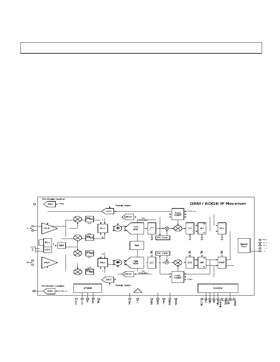
Figure 1. AD6650 Functional Block Diagram

Preliminary Technical Data AD6650
REV. PrJ 02/27/2003 2
TABLE OF CONTENTS
FEATURES . . . . . . . . . . . . . . . . . . . . . . . . . . . . . . . . . . . . xx
PRODUCT DESCRIPTION . . . . . . . . . . . . . . . . . . . . . . . .xx
FUNCTIONAL BLOCK DIAGRAM . . . . . . . . . . . . . . .. .xx
SPECIFICATIONS/CHARACTERISTICS . . . . . .. . . . . . xx
TIMING DIAGRAMS . . . . . . . . . . . . . . . . . . . . . . . . . . . . xx
ABSOLUTE MAXIMUM RATINGS . . . . . . . . . . . . . . . .xx
PIN FUNCTION DESCRIPTIONS . . . . . . . . . . . . . . . . xx
ARCHITECTURE . . . . . . . . . . . . . . . . . . . . . . . . . . . . . . .xx
EXAMPLE FILTER RESPONSE . . . . . . . . . . . . . . . . . . .xx
AGC LOOP.......................................................................xx
DC CORRECTION...........................................................xx
FOURTH ORDER CASCADED INTEGRATOR COMB
FILTER . . . . . . . . . . . . . . . . . . . . . . . . . . . . . . . . . . . . . xx
CIC4 Rejection . . . . . . . . . . . . . . . . . . . . . . . . . . . . . . . xx
INFINITE IMPULSE RESPONSE xx
RAM COEFFICIENT FILTER . . . . . . . . . . . . . . . . . . . . .xx
RCF Decimation Register . . . . . . .. . . . . .. . . . . xx
RCF Decimation Phase . . . . .. . . . . . . . . . . . . . xx
RCF Filter Length . . . . . .. . . . . . . . . . . . . . . . . .xx
RCF Output Scale Factor and Control Register . xx
USER-CONFIGURABLE BUILT-IN SELF-TEST
CHANNEL BIST...........................................xx
CHIP SYNCHRONIZATION . . . . . . . . . . . . . . . . . . . . .xx
Start . . . . . . . . . . . . . . . . .. . . . . . . . . . . . . . . . xx
SERIAL OUTPUT DATA PORT . . . . . . . . . . . . . . . . . . .xx
Serial Output Data Format . . . . . . . . . . . . . . . . . xx
Serial Data Frame (Serial Bus Master) .. . . . . . . . xx
Serial Data Frame (Serial Cascade) . . . . . . . . . xx
Configuring the Serial Ports . . . . . . . .. . . . . . . xx
Serial Port Data Rate . . . . . . . . . .. . . . . . . . . . . . xx
Serial Slave Operation . . . . . . . . . .. . . . . . . . . . . xx
Serial Ports Cascaded . . . . . . . .. . . . . . . . . . . . . . xx
Serial Output Frame Timing (Master and Slave) xx
Serial Port Timing Specifications . . . . . . ... . . . . xx
SCLK . . . . . . . .. . . . . . . . . . . . . . . . . . . . . . . . xx
SDO0 . . . . . . . . . . . . . . . . .. . . . . . . . . . . . . . xx
SDO1 . . . . . . . . . . . . . .. . . . . . . . . . . . . . . . xx
SDFS . . . . . . . . . . . . . .. . . . . . . . . . . . . . . . . . .. . xx
Serial Word Length . . . . . .. . . . . . . . . . . . . . . . . xx
SDFS Mode . . . . . . . . . . . . .. . . . . . . . . . . . . . . . xx
Mapping RCF Data to the BIST Registers . . . .. . xx
0x00: Clock Divider Control . .. . .xx
0x01-0x05: PLL Register[4:0] . . . . . . .. . . . . .. . xx
0x06: Clamp Control............................................xx
0x07: Aux DAC A ...............................................xx
0x08: Aux DAC B ................................................xx
0x09: Aux DAC Control.......................................xx
0x0A: ADC Dither Control.................................xx
0x0B: DC Correction BW.....................................xx
0x0C: DC Correction Control...............................xx
0x0D-0x14: AGC Control[7:0]............................xx
0x15: Start Hold-Off Counter...............................xx
0x16: CIC4 Decimation.......................................xx
0x17: CIC4 Scale.................................................xx
0x18: IIR Control Register...................................xx
0x19: RCF Decimation Register..........................xx
0x1A: RCF Decimation Phase..............................xx
0x1B: RCF Coefficient Offset..............................xx
0x1C: RCF Taps....................................................xx
0x1D: RCF Scale Register...................................xx
0x1E-0x1F: BIST For A-I/Q.................................xx
0x20-0x21: BIST for B-I/Q..................................xx
0x22: Serial Control Register...............................xx
0x23-0x29: Reserved............................................xx
0x30-0x5F: Coefficient Memory.........................xx
0x60-0xFF: Reserved...........................................xx
MICROPORT CONTROL . . . . . . . . . . . . . . . . . . . . . . . . xx
External Memory Map . . . . . .. . . . . . . . . . . . . . . xx
Access Control Register (ACR) . . . . .. . . . . . . . . xx
External Memory Map . . . . . . ... . . . . . . . . . . . . xx
Channel Address Register (CAR) . .. . . . . . . . . . xx
SOFT_SYNC Control Register . .. . . . . . . . . . xx
PIN_SYNC Control Register . . . ... . . . . . . . . . xx
SLEEP Control Register . . . . . . .. . . . . . . . . . . . xx
Data Address Registers . . . . . . .. . . . . . . . . . . . . xx
Write Sequencing . . . . . . . .. . . . . . . . . . . . . . . . . xx
Read Sequencing . . . . . . . .. . . . . . . . . . . . . . . . . xx
Read/Write Chaining . . . . .. . . . . . . . . . . . . . . . . xx
Intel Nonmultiplexed Mode (INM) . . . . . . . . . . . xx
Motorola Nonmultiplexed Mode (MNM) ... . . . . xx
I
2
C PORT CONTROL
JTAG BOUNDARY SCAN . . . . . . . . . . . . . . . . . . . . .xx
INTERNAL WRITE ACCESS . . . . . . . . . . . . . . . .. . . . .xx
Write Pseudocode . . . . . . . . . . . . . . . . . . . . . . . . . . . . . . xx
INTERNAL READ ACCESS . . . . . . . . . . . . . . . . . . . . . . xx
Read Pseudocode . . . . . . . . . . . . . . . . . . . . . . . xx
OUTLINE DIMENSIONS . . . . . . . . . . . . . .. . . . . xx

Preliminary Technical Data AD6650
REV. PrJ 02/27/2003 5
DIGITAL SPECIFICATIONS
(
TMIN
to
TMA
X, AVDD, CLKVDD, DVDD = +3.3v, unless otherwise noted)
Parameter
Temp
Test
Level
MIN
AD6650BBC
Typ
Max
Units
VDD
IV
3.0
3.3
3.6
V
VDDIO
IV
3.0
3.3
3.6
V
AVDD
IV
3.0
3.3
3.6
V
T
AMBIENT
IV
-40
+25
+85
∞C
ELECTRICAL CHARACTERISTICS
Parameter (Conditions)
Temp
Test
Level
Min
AD6650BBC
Typ
Max
Units
LOGIC INPUTS
Logic Compatibility
Full
3.3V CMOS
Logic "1" Voltage
VDD-0.9
VDD
V
Logic "0" Voltage
0
0.9
V
Logic "1" Current
≠10
+10
µA
Logic "0" Current
≠10
10
µA
Input Capacitance
5
pF
LOGIC OUTPUTS
Logic Compatibility
Full
3.3VCMOS/TTL
Logic "1" Voltage (I
OH
=0.25mA) Full
IV
2.4
VDD-0.2
V
Logic "0" Voltage (I
OL
=0.25mA) Full
IV
0.2
0.4
V
IDD SUPPLY CURRENT
CLK=104 MHz (GSM Example)
+25
∞C V
I
VDD
mA
I
VDDIO
mA
I
AVDD
mA
POWER DISSIPATION
CLK=104 MHz GSM/EDGE Example
V
1.2
W