 | –≠–ª–µ–∫—Ç—Ä–æ–Ω–Ω—ã–π –∫–æ–º–ø–æ–Ω–µ–Ω—Ç: AD670S | –°–∫–∞—á–∞—Ç—å:  PDF PDF  ZIP ZIP |
FUNCTIONAL BLOCK DIAGRAM
REV. A
Information furnished by Analog Devices is believed to be accurate and
reliable. However, no responsibility is assumed by Analog Devices for its
use, nor for any infringements of patents or other rights of third parties
which may result from its use. No license is granted by implication or
otherwise under any patent or patent rights of Analog Devices.
a
Low Cost Signal
Conditioning 8-Bit ADC
AD670
FEATURES
Complete 8-Bit Signal Conditioning A/D Converter
Including Instrumentation Amp and Reference
Microprocessor Bus Interface
10 s Conversion Speed
Flexible Input Stage: Instrumentation Amp Front End
Provides Differential Inputs and High Common-Mode
Rejection
No User Trims Required
No Missing Codes Over Temperature
Single +5 V Supply Operation
Convenient Input Ranges
20-Pin DIP or Surface-Mount Package
Low Cost Monolithic Construction
MIL-STD-883B Compliant Versions Available
GENERAL DESCRIPTION
The AD670 is a complete 8-bit signal conditioning analog-
to-digital converter. It consists of an instrumentation amplifier
front end along with a DAC, comparator, successive approxima-
tion register (SAR), precision voltage reference, and a three-
state output buffer on a single monolithic chip. No external
components or user trims are required to interface, with full
accuracy, an analog system to an 8-bit data bus. The AD670
will operate on the +5 V system supply. The input stage pro-
vides differential inputs with excellent common-mode rejection
and allows direct interface to a variety of transducers.
The device is configured with input scaling resistors to permit
two input ranges: 0 mV to 255 mV (1 mV/LSB) and 0 to 2.55 V
(10 mV/LSB). The AD670 can be configured for both unipolar
and bipolar inputs over these ranges. The differential inputs and
common-mode rejection of this front end are useful in applica-
tions such as conversion of transducer signals superimposed on
common-mode voltages.
The AD670 incorporates advanced circuit design and proven
processing technology. The successive approximation function
is implemented with I
2
L (integrated injection logic). Thin-film
SiCr resistors provide the stability required to prevent missing
codes over the entire operating temperature range while laser
wafer trimming of the resistor ladder permits calibration of the
device to within
±
1 LSB. Thus, no user trims for gain or offset
are required. Conversion time of the device is 10
µ
s.
The AD670 is available in four package types and five grades.
The J and K grades are specified over 0
∞
C to +70
∞
C and come
in 20-pin plastic DIP packages or 20-terminal PLCC packages.
The A and B grades (≠40
∞
C to +85
∞
C) and the S grade (≠55
∞
C
to +125
∞
C) come in 20-pin ceramic DIP packages.
One Technology Way, P.O. Box 9106, Norwood, MA 02062-9106, U.S.A.
Tel: 617/329-4700
Fax: 617/326-8703
The S grade is also available with optional processing to
MIL-STD-883 in 20-pin ceramic DIP or 20-terminal LCC
packages. The Analog Devices Military Products Databook
should be consulted for detailed specifications.
PRODUCT HIGHLIGHTS
1. The AD670 is a complete 8-bit A/D including three-state
outputs and microprocessor control for direct connection to
8-bit data buses. No external components are required to
perform a conversion.
2. The flexible input stage features a differential instrumenta-
tion amp input with excellent common-mode rejection. This
allows direct interface to a variety of transducers without
preamplification.
3. No user trims are required for 8-bit accurate performance.
4. Operation from a single +5 V supply allows the AD670 to
run off of the microprocessor's supply.
5. Four convenient input ranges (two unipolar and two bipolar)
are available through internal scaling resistors: 0 mV to
255 mV (1 mV/LSB) and 0 V to 2.55 V (10 mV/LSB).
6. Software control of the output mode is provided. The user
can easily select unipolar or bipolar inputs and binary or 2s
complement output codes.

Model
AD670J
AD670K
Min
Typ
Max
Min
Typ
Max
Units
OPERATING TEMPERATURE RANGE
0
+70
0
+70
∞
C
RESOLUTION
8
8
Bit
CONVERSION TIME
10
10
µ
s
RELATIVE ACCURACY
1/2
1/4
LSB
T
MIN
to T
MAX
l/2
1/2
LSB
DIFFERENTIAL LINEARITY ERROR
1
T
MIN
to T
MAX
GUARANTEED NO MISSING CODES ALL GRADES
GAIN ACCURACY
@ +25
∞
C
1.5
0.75
LSB
T
MIN
to T
MAX
2.0
1.0
LSB
UNIPOLAR ZERO ERROR
@ +25
∞
C
1.5
0.75
LSB
T
MIN
to T
MAX
2.0
1.0
LSB
BIPOLAR ZERO ERROR
@ +25
∞
C
1.5
0.75
LSB
T
MIN
to T
MAX
2.0
1.0
LSB
ANALOG INPUT RANGES
DIFFERENTIAL (≠V
IN
to +V
IN
)
Low Range
0 to +255
0 to +255
mV
≠128 to +127
≠128 to +127
mV
High Range
0 to +2.55
0 to +2.55
V
≠1.28 to +1.27
≠1.28 to +1.27
V
ABSOLUTE (Inputs to Power GND)
Low Range T
MIN
to T
MAX
≠0.150
V
CC
≠ 3.4
≠0.150
V
CC
≠ 3.4
V
High Range T
MIN
to T
MAX
≠1.50
V
CC
≠1.50
V
CC
V
BIAS CURRENT (255 mV RANGE)
T
MIN
to T
MAX
200
500
200
500
nA
OFFSET CURRENT (255 mV RANGE)
T
MIN
to T
MAX
40
200
40
200
nA
2.55 V RANGE INPUT RESISTANCE
8.0
12.0
8.0
12.0
k
2.55 V RANGE FULL-SCALE MATCH
+ AND ≠ INPUT
±
1/2
±
1/2
LSB
COMMON-MODE REJECTION
RATIO (255 mV RANGE)
1
1
LSB
COMMON-MODE REJECTION
RATIO (2.55 V RANGE)
1
1
LSB
POWER SUPPLY
Operating Range
4.5
5.5
4.5
5.5
V
Current I
CC
30
45
30
45
mA
Rejection Ratio T
MIN
to T
MAX
0.015
0.015
% of FS/%
DIGITAL OUTPUTS
SINK CURRENT (V
OUT
= 0.4 V)
T
MIN
to T
MAX
1.6
1.6
mA
SOURCE CURRENT (V
OUT
= 2.4 V)
T
MIN
to T
MAX
0.5
0.5
mA
THREE-STATE LEAKAGE CURRENT
40
40
µ
A
OUTPUT CAPACITANCE
5
5
pF
DIGITAL INPUT VOLTAGE
V
INL
0.8
0.8
V
V
INH
2.0
2.0
V
DIGITAL INPUT CURRENT
(0
V
IN
+5 V)
I
INL
≠100
≠100
µ
A
I
INH
+100
+100
µ
A
INPUT CAPACITANCE
10
10
pF
NOTES
1
Tested at V
CC
= 4 5 V, 5.0 V and 5.5 V.
Specifications shown in boldface are tested on all production units at final electrical test. Results from those tests are used to calculate outgoing quality levels. All min and max specifications
are guaranteed although only those shown in boldface are tested on all production units.
Specifications subject to change without notice.
AD670≠SPECIFICATIONS
(@ V
CC
= +5 V and +25 C, unless otherwise noted)
REV. A
≠2≠

Model
AD670A
AD670B
AD670S
Min
Typ
Max
Min
Typ
Max
Min
Typ
Max
Units
OPERATING TEMPERATURE RANGE
≠40
+85
≠40
+85
≠55
+125
∞
C
RESOLUTION
8
8
8
Bit
CONVERSION TIME
10
10
10
µ
s
RELATIVE ACCURACY
1/2
1/4
1/2
LSB
T
MIN
to T
MAX
1/2
1/2
1
LSB
DIFFERENTIAL LINEARITY ERROR
1
T
MIN
to T
MAX
GUARANTEED NO MISSING CODES ALL GRADES
GAIN ACCURACY
@ +25
∞
C
1.5
0.75
1.5
LSB
T
MIN
to T
MAX
2.5
1.5
2.5
LSB
UNIPOLAR ZERO ERROR
@ +25
∞
C
1.0
0.5
1.0
LSB
T
MIN
to T
MAX
2.0
1.0
2.0
LSB
BIPOLAR ZERO ERROR
@ +25
∞
C
1.0
0.5
1.0
LSB
T
MIN
to T
MAX
2.0
1.0
2.0
LSB
ANALOG INPUT RANGES
DIFFERENTIAL ( ≠V
IN
to +V
IN
)
Low Range
0 to +255
0 to +255
0 to +255
mV
≠128 to +127
≠128 to +127
≠128 to +127
mV
High Range
0 to +2.55
0 to +2.55
0 to +2.55
V
≠1.28 to +1.27
≠1.28 to +1.27
≠1.28 to +1.27
V
ABSOLUTE (Inputs to Power GND)
Low Range T
MIN
to T
MAX
≠0.150
V
CC
≠ 3.5 ≠0.150
V
CC
≠ 3.5
≠0.150
V
CC
≠ 3.5
V
High Range T
MIN
to T
MAX
≠1.50
V
CC
≠1.50
V
CC
≠1.50
V
CC
V
BIAS CURRENT (255 mV RANGE)
T
MIN
to T
MAX
200
500
200
500
200
750
nA
OFFSET CURRENT (255 mV RANGE)
T
MIN
to T
MAX
40
200
40
200
40
200
nA
2.55 V RANGE INPUT RESISTANCE
8.0
12.0
8.0
12.0
8.0
12.0
k
2.55 V RANGE FULL-SCALE MATCH
+ AND ≠ INPUT
±
1/2
±
1/2
±
1/2
LSB
COMMON-MODE REJECTION
RATIO (255 mV RANGE)
1
1
1
LSB
COMMON-MODE REJECTION
RATIO (2.55 V RANGE)
1
1
1
LSB
POWER SUPPLY
Operating Range
4.5
5.5
4.5
5.5
4.75
5.5
V
Current I
CC
30
45
30
45
30
45
mA
Rejection Ratio T
MIN
to T
MAX
0.015
0.015
0.015
% of FS/%
DIGITAL OUTPUTS
SINK CURRENT (V
OUT
= 0.4 V)
T
MIN
to T
MAX
1.6
1.6
1.6
mA
SOURCE CURRENT (V
OUT
= 2.4 V)
T
MIN
to T
MAX
0.5
0.5
0.5
mA
THREE-STATE LEAKAGE CURRENT
40
40
40
µ
A
OUTPUT CAPACITANCE
5
5
5
pF
DIGITAL INPUT VOLTAGE
V
INL
0.8
0.8
0.7
V
V
INH
2.0
2.0
2.0
V
DIGITAL INPUT CURRENT
(0
V
IN
+5 V)
I
INL
≠100
≠100
≠100
µ
A
I
INH
+100
+100
+ 100
µ
A
INPUT CAPACITANCE
10
10
10
pF
NOTES
1
Tested at V
CC
= 4.5 V, 5.0 V and 5.5 V for A, B grades; 4.75 V, 5.0 V and 5.5 V for S grade.
Specifications shown in boldface are tested on all production units at final electrical test. Results from those tests are used to calculate outgoing quality levels. All min and max specifications
are guaranteed, although only those shown in boldface are tested on all production units.
Specifications subject to change without notice.
AD670
REV. A
≠3≠

AD670
REV. A
≠4≠
ORDERING GUIDE
Temperature
Relative Accuracy
Gain Accuracy
Model
1
Range
@ +25 C
@ +25 C
Package Option
2
AD670JN
0
∞
C to +70
∞
C
±
1/2 LSB
±
1.5 LSB
Plastic DIP (N-20)
AD670JP
0
∞
C to +70
∞
C
±
1/2 LSB
±
1.5 LSB
PLCC (P-20A)
AD670KN
0
∞
C to +70
∞
C
±
1/4 LSB
±
0.75 LSB
Plastic DIP (N-20)
AD670KP
0
∞
C to +70
∞
C
±
1/4 LSB
±
0.75 LSB
PLCC (P-20A)
AD670AD
≠40
∞
C to +85
∞
C
±
1/2 LSB
±
1.5 LSB
Ceramic DIP (D-20)
AD670BD
≠40
∞
C to +85
∞
C
±
1/4 LSB
±
0.75 LSB
Ceramic DIP (D-20)
AD670SD
≠55
∞
C to +125
∞
C
±
1/2 LSB
±
1.5 LSB
Ceramic DIP (D-20)
NOTES
1
For details on grade and package offerings screened in accordance with MIL-STD-883 refer to the Analog Devices
Military Products Databook.
2
D = Ceramic DIP; N = Plastic DIP; P = Plastic Leaded Chip Carrier.
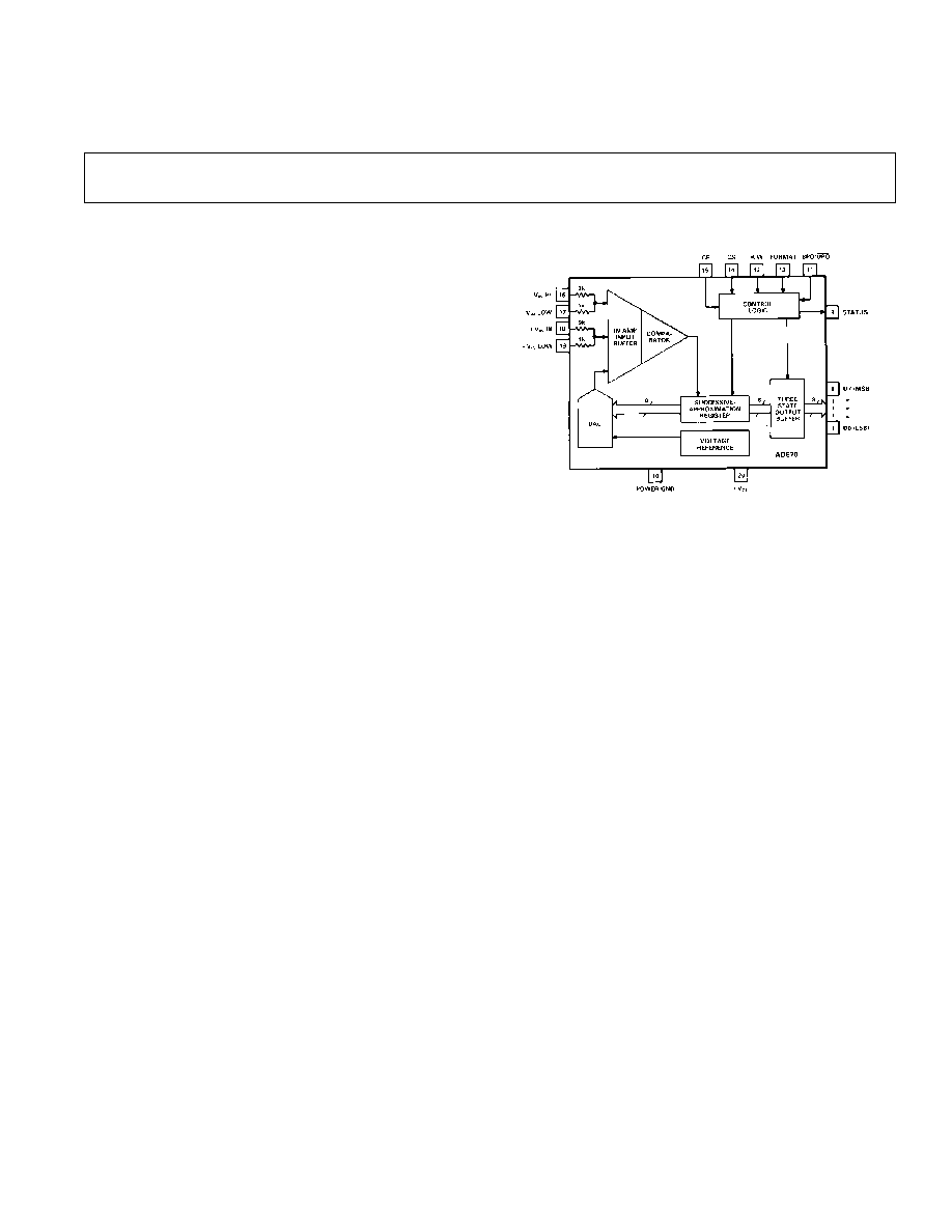
Figure 1. AD670 Block Diagram and Terminal
Configuration (AII Packages)
ABSOLUTE MAXIMUM RATINGS*
V
CC
to Ground . . . . . . . . . . . . . . . . . . . . . . . . . . . 0 V to +7.5 V
Digital Inputs (Pins 11≠15) . . . . . . . . . . . ≠0.5 V to V
CC
+0.5 V
Digital Outputs (Pins 1≠9) . Momentary Short to V
CC
or Ground
Analog Inputs (Pins 16≠19) . . . . . . . . . . . . . . . ≠30 V to +30 V
Power Dissipation . . . . . . . . . . . . . . . . . . . . . . . . . . . . 450 mW
Storage Temperature Range . . . . . . . . . . . . . ≠65
∞
C to +150
∞
C
Lead Temperature (Soldering, 10 sec) . . . . . . . . . . . . . +300
∞
C
*Stresses above those listed under "Absolute Maximum Ratings" may cause
permanent damage to the device. This is a stress rating only and functional
operation of the device at them or any other conditions above those indicated in
the operational sections of this specification is not implied. Exposure to absolute
maximum rating conditions for extended periods may affect device reliability.
CIRCUIT OPERATION/FUNCTIONAL DESCRIPTION
The AD670 is a functionally complete 8-bit signal conditioning
A/D converter with microprocessor compatibility. The input
section uses an instrumentation amplifier to accomplish the
voltage to current conversion. This front end provides a high
impedance, low bias current differential amplifier. The com-
mon-mode range allows the user to directly interface the device
to a variety of transducers.
The AID conversions are controlled by R/W, CS, and CE. The
R/W line directs the converter to read or start a conversion. A
minimum write/start pulse of 300 ns is required on either CE or
CS
. The STATUS line goes high, indicating that a conversion is
in process. The conversion thus begun, the internal 8-bit DAC
is sequenced from MSB to LSB using a novel successive ap-
proximation technique. In conventional designs, the DAC is
stepped through the bits by a clock. This can be thought of as a
static design since the speed at which the DAC is sequenced is
determined solely by the clock. No clock is used in the AD670.
Instead, a "dynamic SAR" is created consisting of a string of in-
verters with taps along the delay line. Sections of the delay line
between taps act as one shots. The pulses are used to set and re-
set the DAC's bits and strobe the comparator. When strobed,
the comparator then determines whether the addition of each
successively weighted bit current causes the DAC current sum
to be greater or less than the input current. If the sum is less,
the bit is turned off. After all bits are tested, the SAR holds an
8-bit code representing the input signal to within 1/2 LSB
accuracy. Ease of implementation and reduced dependence on
process related variables make this an attractive approach to a
successive approximation design.
The SAR provides an end-of-conversion signal to the control
logic which then brings the STATUS line low. Data outputs re-
main in a high impedance state until R/W is brought high with
CE
and CS low and allows the converter to be read. Bringing
CE
or CS high during the valid data period ends the read cycle.
The output buffers cannot be enabled during a conversion. Any
convert start commands will be ignored until the conversion
cycle is completed; once a conversion cycle has been started it
cannot be stopped or restarted.
The AD670 provides the user with a great deal of flexibility by
offering two input spans and formats and a choice of output
codes. Input format and input range can each be selected. The
BPO/UPO pin controls a switch which injects a bipolar offset
current of a value equal to the MSB less 1/2 LSB into the sum-
ming node of the comparator to offset the DAC output. Two
precision 10 to 1 attenuators are included on board to provide
input range selection of 0 V to 2.55 V or 0 mV to 255 mV. Ad-
ditional ranges of ≠1.28 V to 1.27 V and ≠128 mV to 127 mV
are possible if the BPO/UPO switch is high when the conversion
is started. Finally, output coding can be chosen using the FOR-
MAT pin when the conversion is started. In the bipolar mode
and with a Logic 1 on FORMAT, the output is in two's comple-
ment; with a Logic 0, the output is offset binary.

AD670
REV. A
≠5≠
CONNECTING THE AD670
The AD670 has been designed for ease of use. All active com-
ponents required to perform a complete A/D conversion are on
board and are connected internally. In addition, all calibration
trims are performed at the factory, assuring specified accuracy
without user trims. There are, however, a number of options
and connections that should be considered to obtain maximum
flexibility from the part.
INPUT CONNECTIONS
Standard connections are shown in the figures that follow. An
input range of 0 V to 2.55 V may be configured as shown in Fig-
ure 2a. This will provide a one LSB change for each 10 mV of
input change. The input range of 0 mV to 255 mV is configured
as shown in Figure 2b. In this case, each LSB represents 1 mV
of input change. When unipolar input signals are used, Pin 11,
BPO/UPO, should be grounded. Pin 11 selects the input format
for either unipolar or bipolar signals. Figures 3a and 3b show
the input connections for bipolar signals. Pin 11 should be tied
to +V
CC
for bipolar inputs.
Although the instrumentation amplifier has a differential input,
there must be a return path to ground for the bias currents. If it
is not provided, these currents will charge stray capacitances
and cause internal circuit nodes to drift uncontrollably causing
the digital output to change. Such a return path is provided in
Figures 2a and 3a (larger input ranges) since the 1k resistor leg
is tied to ground. This is not the case for Figures 2b and 3b (the
lower input ranges). When connecting the AD670 inputs to
floating sources, such as transformers and ac-coupled sources,
there must still be a dc path from each input to common. This
can be accomplished by connecting a 10 k
resistor from each
input to ground.
2a. 0 V to 2.55 V (10 mV/LSB)
2b. 0 mV to 255 mV (1 mV/LSB)
NOTE: PIN 11, BPO/UPO SHOULD BE LOW WHEN
CONVERSION IS STARTED.
Figure 2. Unipolar Input Connections
3a.
±
1.28 V Range
3b.
±
128 mV Range
NOTE: PIN 11, BPO/UPO SHOULD BE HIGH WHEN
CONVERSION IS STARTED.
Figure 3. Bipolar Input Connections
Bipolar Operation
Through special design of the instrumentation amplifier, the
AD670 accommodates input signal excursions below ground,
even though it operates from a single 5 V supply. To the user,
this means that true bipolar input signals can be used without
the need for any additional external components. Bipolar signals
can be applied differentially across both inputs, or one of the in-
puts can be grounded and a bipolar signal applied to the other.
Common-Mode Performance
The AD670 is designed to reject dc and ac common-mode volt-
ages. In some applications it is useful to apply a differential in-
put signal V
IN
in the presence of a dc common-mode voltage
V
CM
. The user must observe the absolute input signal limits
listed in the specifications, which represent the maximum volt-
age V
IN
+ V
CM
that can be applied to either input without affect-
ing proper operation. Exceeding these limits (within the range of
absolute maximum ratings), however, will not cause permanent
damage.
The excellent common-mode rejection of the AD670 is due to
the instrumentation amplifier front end, which maintains the
differential signal until it reaches the output of the comparator.
In contrast to a standard operational amplifier, the instrumenta-
tion amplifier front end provides significantly improved CMRR
over a wide frequency range (Figure 4a).

AD670
REV. A
≠6≠
Table I. AD670 Input Selection/Output Format Truth Table
INPUT RANGE/
BPO/UPO
FORMAT
OUTPUT FORMAT
0
0
Unipolar/Straight Binary
1
0
Bipolar/Offset Binary
0
1
Unipolar/2s Complement
1
1
Bipolar/2s Complement
DIFF
STRAIGHT BINARY
+V
IN
≠V
IN
V
IN
(FORMAT = 0, BPO/UPO = 0)
0
0
0
0000 0000
128 mV
0
128 mV
1000 0000
255 mV
0
255 mV
1111 1111
255 mV
255 mV
0
0000 0000
128 mV
127 mV
1 mV
0000 0001
128 mV
≠127 mV
255 mV
1111 1111
Figure 5a. Unipolar Output Codes (Low Range)
OFFSET BINARY 2s COMPLEMENT
DIFF
(FORMAT = 0,
(FORMAT = 1,
+V
IN
≠V
IN
V
IN
BPO/UPO = 1)
BPO/UPO = 1)
0
0
0
1000 0000
0000 0000
127 mV
0
127 mV
1111 1111
0111 1111
1.127 V
1.000 V
127 mV
1111 1111
0111 1111
255 mV
255 mV
0
1000 0000
0000 0000
128 mV
127 mV
1 mV
1000 0001
0000 0001
127 mV
128 mV
≠1 mV
0111 1111
1111 1111
127 mV
255 mV
≠128 mV
0000 0000
1000 0000
≠128 mV 0
≠128 mV
0000 0000
1000 0000
Figure 5b. Bipolar Output Codes (Low Range)
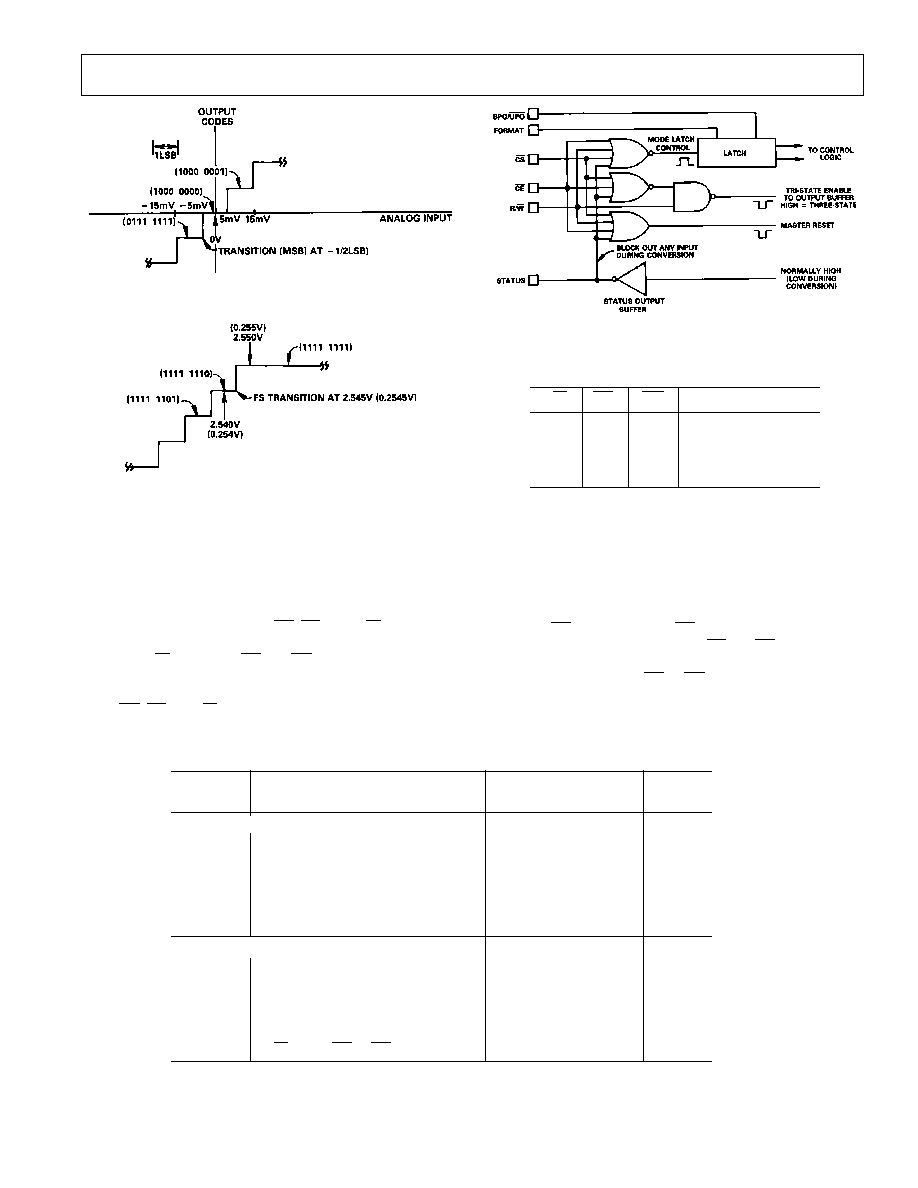
Calibration
Because of its precise factory calibration, the AD670 is intended
to be operated without user trims for gun and offset; therefore,
no provisions have been made for such user trims. Figures 6a,
6b, and 6c show the transfer curves at zero and full scale for the
unipolar and bipolar modes. The code transitions are positioned
so that the desired value is centered at that code. The first LSB
transition for the unipolar mode occurs for an input of +1/2 LSB
(5 mV or 0.5 mV). Similarly, the MSB transition for the bipolar
mode is set at ≠1/2 LSB (≠5 mV or ≠0.5 mV). The full scale
transition is located at the full scale value ≠1 1/2 LSB. These
values are 2.545 V and 254.5 mV.
6a. Unipolar Transfer Curve
Figure 4a. CMRR Over Frequency
Figure 4b. AD670 Input Rejects Common-Mode
Ground Noise
Good common-mode performance is useful in a number of situ-
ations. In bridge-type transducer applications, such performance
facilitates the recovery of differential analog signals in the pres-
ence of a dc common-mode or a noisy electrical environment.
High frequency CMRR also becomes important when the ana-
log signal is referred to a noisy, remote digital ground. In each
case, the CMRR specification of the AD670 allows the integrity
of the input signal to be preserved.
The AD670's common-mode voltage tolerance allows great
flexibility in circuit layout. Most other A/D converters require
the establishment of one point as the analog reference point.
This is necessary in order to minimize the effects of parasitic
voltages. The AD670, however, eliminates the need to make the
analog ground reference point and A/D analog ground one and
the same. Instead, a system such as that shown in Figure 4b is
possible as a result of the AD670's common-mode performance.
The resistors and inductors in the ground return represent un-
avoidable system parasitic impedances.
Input/Output Options
Data output coding (2s complement vs. straight binary) is
selected using Pin 12, the FORMAT pin. The selection of
input format (bipolar vs. unipolar) is controlled using Pin 11,
BPO/UPO. Prior to a write/convert, the state of FORMAT and
BPO/UPO should be available to the converter. These lines may
be tied to the data bus and may be changed with each conver-
sion if desired. The configurations are shown in Table I. Output
coding for representative signals in each of these configurations
is shown in Figure 5.
An output signal, STATUS, indicates the status of the conver-
sion. STATUS goes high at the beginning of the conversion and
returns low when the conversion cycle has been completed.
AD670
REV. A
≠7≠
Table III. AD670 TIMING SPECIFICATIONS
@ +25 C
Symbol
Parameter
Min
Typ
Max
Units
WRITE/CONVERT START MODE
t
W
Write/Start Pulse Width
300
ns
t
DS
Input Data Setup Time
200
ns
t
DH
Input Data Hold
10
ns
t
RWC
Read/Write Setup Before Control
0
ns
t
DC
Delay to Convert Start
700
ns
t
C
Conversion Time
10
µ
s
READ MODE
t
R
Read Time
250
ns
t
SD
Delay from Status Low to Data Read
250
ns
t
TD
Bus Access Time
200
250
ns
t
DH
Data Hold Time
25
ns
t
DT
Output Float Delay
150
ns
t
RT
R/W before CE or CS low
0
ns
Boldface indicates parameters tested 100% unless otherwise noted. See Specifications page for explanation.
6b. Bipolar
6c. Full Scale (Unipolar)
Figure 6. Transfer Curves
CONTROL AND TIMING OF THE AD670
Control Logic
The AD670 contains on-chip logic to provide conversion and
data read operations from signals commonly available in micro-
processor systems. Figure 7 shows the internal logic circuitry of
the AD670. The control signals, CE, CS, and R/W control the
operation of the converter. The read or write function is deter-
mined by R/W when both CS and CE are low as shown in
Table II. If all three control inputs are held low longer than the
conversion time, the device will continuously convert until one
input, CE, CS, or R/W is brought high. The relative timing of
these signals is discussed later in this section.
Figure 7. Control Logic Block Diagram
Table II. AD670 Control Signal Truth Table
R/W
CS
CE
OPERATION
0
0
0
WRITE/CONVERT
1
0
0
READ
X
X
1
NONE
X
1
X
NONE
Timing
The AD670 is easily interfaced to a variety of microprocessors
and other digital systems. The following discussion of the timing
requirements of the AD670 control signals will provide the de-
signer with useful insight into the operation of the device.
Write/Convert Start Cycle
Figure 8 shows a complete timing diagram for the write/convert
start cycle. CS (chip select) and CE (chip enable) are active low
and are interchangeable signals. Both CS and CE must be low
for the converter to read or start a conversion. The minimum
pulse width, t
W
, on either CS or CE is 300 ns to start a
conversion.

AD670
REV. A
≠8≠
Figure 8. Write/Convert Start Timing
The R/W line is used to direct the converter to start a conver-
sion (R/W low) or read data (R/W high). The relative sequenc-
ing of the three control signals (R/W, CE, CS) is unimportant.
However, when all three signals remain low for at least 300 ns
(t
W
), STATUS will go high to signal that a conversion is taking
place.
Once a conversion is started and the STATUS line goes high,
convert start commands will be ignored until the conversion
cycle is complete. The output data buffer cannot be enabled
during a conversion.
Read Cycle
Figure 9 shows the timing for the data read operation. The data
outputs are in a high impedance state until a read cycle is initi-
ated. To begin the read cycle, R/W is brought high. During a
read cycle, the minimum pulse length for CE and CS is a func-
tion of the length of time required for the output data to be
valid. The data becomes valid and is available to the data bus in
a maximum of 250 ns. This delay between the high impedance
state and valid data is the maximum bus access time or t
TD
.
Bringing CE or CS high during valid data ends the read cycle.
The outputs remain valid for a minimum of 25 ns (t
DH
) and re-
turn to the high impedance state after a delay, t
DT
, of 150 ns
maximum.
Figure 9. Read Cycle Timing
STAND-ALONE OPERATION
The AD670 can be used in a "stand-alone" mode, which is use-
ful in systems with dedicated input ports available. Two typical
conditions are described and illustrated by the timing diagrams
which follow.
Single Conversion, Single Read
When the AD670 is used in a stand-alone mode, CS and CE
should be tied together. Conversion will be initiated by bringing
R/W low. Within 700 ns, a conversion will begin. The R/W
pulse should be brought high again once the conversion has
started so that the data will be valid upon completion of the
conversion. Data will remain valid until CE and CS are brought
high to indicate the end of the read cycle or R/W goes low. The
timing diagram is shown in Figure 10.
Figure 10. Stand-Alone Mode Single Conversion/
Single Read
Continuous Conversion, Single Read
A variety of applications may call for the A/D to be read after
several conversions. In process control systems, this is often the
case since a reading from a sensor may only need to be updated
every few conversions. Figure 11 shows the timing relationships.
Once again, CE and CS should be tied together. Conversion
will begin when the R/W signal is brought low. The device will
convert repeatedly as indicated by the status line. A final con-
version will take place once the R/W line has been brought high.
The rising edge of R/W must occur while STATUS is high. R/W
should not return high while STATUS is low since the circuit is
in a reset state prior to the next conversion. Since the rising
edge of R/W must occur while STATUS is high, R/W's length
must be a minimum of 10.25
µ
s (t
C
+ t
TD
). Data becomes valid
upon completion of the conversion and will remain so until the
CE
and CS lines are brought high indicating the end of the read
cycle or R/W goes low initiating a new series of conversions.
Figure 11. Stand-Alone Mode Continuous Conversion/
Single Read

AD670
REV. A
≠9≠
APPLYING THE AD670
The AD670 has been designed for ease of use, system compat-
ibility, and minimization of external components. Transducer
interfaces generally require signal conditioning and preampli-
fication before the signal can be converted. The AD670 will
reduce and even eliminate this excess circuitry in many cases.
To illustrate the flexibility and superior solution that the AD670
can bring to a transducer interface problem, the following dis-
cussions are offered.
Temperature Measurements
Temperature transducers are one of the most common sources
of analog signals in data acquisition systems. These sensors re-
quire circuitry for excitation and preamplification/buffering. The
instrumentation amplifier input of the AD670 eliminates the
need for this signal conditioning. The output signals from tem-
perature transducers are generally sufficiency slow that a
sample/hold amplifier is not required. Figure 12 shows tile
AD590 IC temperature transducer interfaced to the AD670.
The AD580 voltage reference is used to offset the input for 0
∞
C
calibration. The current output of the AD590 is converted into
a voltage by R1. The high impedance unbuffered voltage is ap-
plied directly to the AD670 configured in the ≠128 mV to
127 mV bipolar range. The digital output will have a resolution
of 1
∞
C.
Figure 12. AD670 Temperature Transducer lnterface
Platinum RTDs are also a popular, temperature transducer.
Typical RTDs have a resistance of 100
at 0
∞
C and change re-
sistance 0.4
per
∞
C. If a consent excitation current is caused
to flow in the RTD, the change in voltage drop will be a mea-
sure of the change in temperature. Figure 13 shows such a
method and the required connections to the AD670. The
AD580 2.5 V reference provides the accurate voltage for the ex-
citation current and range offsetting for the RTD. The op amp
is configured to force a constant 2.5 mA current through the
RTD. The differential inputs of the AD670 measure the differ-
ence between a fixed offset voltage and the temperature depen-
dent output of the op amp which varies with the resistance of
the RTD. The RTD change of approximately 0.4
/
∞
C results
in a 1 mV/
∞
C voltage change. With the AD670 in the 1 mV/LSB
range, temperatures from 0
∞
C to 255
∞
C can be measured.
Figure 13. Low Cost RTD Interface
Differential temperature measurements can be made using an
AD590 connected to each of the inputs as shown in Figure 14.
This configuration will allow the user to measure the relative
temperature difference between two points with a 1
∞
C resolu-
tion. Although the internal 1k and 9k resistors on the inputs
have
±
20% tolerance, trimming the AD590 is unnecessary as
most differential temperature applications are concerned with
the relative differences between the two. However, the user may
see up to a 20% scale factor error in the differential temperature
to digital output transfer curve.
This scale factor error can be eliminated through a software cor-
rection. Offset corrections can be made by adjusting for any dif-
ference that results when both sensors are held at the same
temperature. A span adjustment can then be made by immers-
ing one AD590 in an ice bath and one in boiling water and
eliminating any deviation from 100
∞
C. For a low cost version of
this setup, the plastic AD592 can be substituted for the AD590.
Figure 14. Differential Temperature Measurement
Using the AD590
~

AD670
REV. A
≠10≠
STRAIN GAGE MEASUREMENTS
Many semiconductor-type strain gages, pressure transducers,
and load cells may also be connected directly to the AD670.
These types of transducers typically produce 30 mV full-scale
per volt of excitation. In the circuit shown in Figure 15, the
AD670 is connected directly to a Data Instruments model JP-20
load cell. The AD584 programmable voltage reference is used
along with an AD741 op amp to provide the
±
2.5 V excitation
for the load cell. The output of the transducer will be
±
150 mV
for a force of
±
20 pounds. The AD670 is configured for the
±
128 millivolt range. The resolution is then approximately 2.1
ounces per LSB over a range of
±
17 pounds. Scaling to exactly
2 ounces per LSB can be accomplished by trimming the refer-
ence voltage which excites the load cell.
Figure 15. AD670 Load Cell Interface
MULTIPLEXED INPUTS
Most data acquisition systems require the measurement of sev-
eral analog signals. Multiple A/D converters are often used to
digitize these inputs, requiring additional preamplification and
buffer stages per channel. Since these signals vary slowly, a dif-
ferential MUX can multiplex inputs from several transducers
into a single AD670. And since the AD670's signal-conditioning
capability is preserved, the cost of several ADCs, differential
amplifiers, and other support components can be reduced to
that of a single AD670, a MUX, and a few digital logic gates.
An AD7502 dual 4-channel MUX appears in Figure 16 multi-
plexing four differential signals to the AD670. The AD7502's
decoded address is gated with the microprocessor's write signal
to provide a latching strobe at the flip-flops. A write cycle to the
AD7502's address then latches the two LSBs of the data word
thereby selecting the input channel for subsequent conversions.
Figure 16. Multiplexed Analog Inputs to AD670
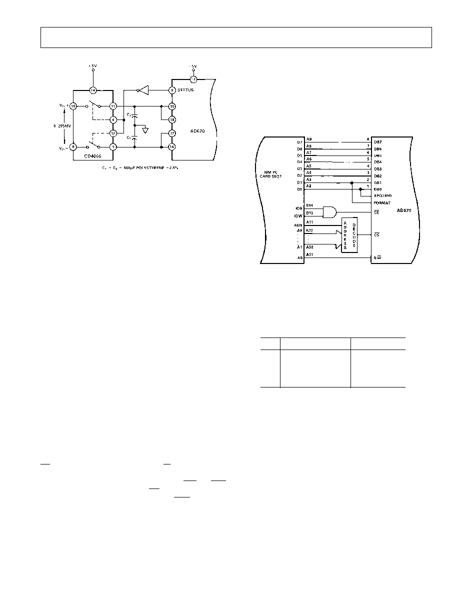
SAMPLED INPUTS
For those applications where the input signal is capable of slew-
ing more than 1/2 LSB during the AD670's 10
µ
s conversion
cycle, the input should be held constant for the cycle's duration.
The circuit shown in Figure 17 uses a CMOS switch and two
capacitors to sample/hold the input. The AD670's STATUS
output, once inverted, supplies the sample/hold (S/H) signal.
A convert command applied on the CE, CS or R/W lines will
initiate the conversion. The AD670's STATUS output, once in-
verted, supplies the sample/hold signal to the CD4066. The
CD4066 CMOS switch shown in Figure 17 was chosen for its
fast transition times, low on-resistance and low cost. The con-
trol input's propagation delay for switch-closed to switch-open
should remain less than 150 ns to ensure that the sample-to-
hold transition occurs before the first bit decision in the AD670.
AD670
REV. A
≠11≠
Figure 17. Low Cost Sample-and-Hold Circuit for AD670
Since settling to 1/2 LSB at 8-bits of resolution requires 6.2 RC
time constants, the 500 pF hold capacitors and CD4066's 300
on-resistance yield an acquisition time of under 1
µ
s, assuming a
low impedance source.
This sample/hold approach makes use of the differential capa-
bilities of the AD670. Because 500 pF hold capacitors are used
on both V
IN
+ and V
IN
≠ inputs, the droop rate depends only on
the offset current of the AD670, typically 20 nA. With the
matched 500 pF capacitors, the droop rate is 40
µ
V/
µ
s. The in-
put will then droop only 0.4 mV (0.4 LSB) during the AD670's
10
µ
s conversion time. The differential approach also minimizes
pedestal error since only the difference in charge injection be-
tween the two switches results in errors at the A/D.
The fast conversion time and differential and common-mode ca-
pabilities of the AD670 permit this simple sample-hold design
to perform well with low sample-to-hold offset, droop rate of
about 40
µ
V/
µ
s and acquisition time under 1
µ
s. The effective
aperture time of the AD670 is reduced by about 2 orders of
magnitude with this circuit, allowing frequencies to be con-
verted up to several kilohertz.
While no input anti-aliasing filter is shown, filtering will be nec-
essary to prevent output errors if higher frequencies are present
in the input signal. Many practical variations are possible with
this circuit, including input MUX control, for digitizing a num-
ber of ac channels.
IBM PC INTERFACE
The AD670 appears in Figure 18 interfaced to the IBM PC.
Since the device resides in I/O space, its address is decoded
from only the lower ten address lines and must be gated with
AEN (active low) to mask out internal (DMA) cycles which use
the same I/O address space. This active low signal is applied to
CS
. AO, meanwhile, is reserved for the R/W input. This places
the AD670 in two adjacent addresses; one for starting the con-
version and the other for reading the result. The IOR and IOW
signals are then gated and applied to CE, while the lower two
data lines are applied to FORMAT and BPO/UPO inputs to
provide software programmable input formats and output
coding.
In BASIC, a simple OUT ADDR, WORD command initiates a
conversion. While the upper six bits of the data WORD are
meaningless, the lower two bits define the analog input format
and digital output coding according to Table IV. The data is
available ten microseconds later (which is negligible in BASIC)
and can be read using INP (ADDR + 1). The 3-line subroutine
in Figure 19, used in conjunction with the interface of Figure
18, converts an analog input within a bipolar range to an offset
binary coded digital word.
Figure 18. IBM PC lnterface to AD670
NOTE: Due to the large number of options that may be in-
stalled in the PC, the I/O bus loading should be limited to one
Schottky TTL load. Therefore, a buffer/driver should be used
when interfacing more than two AD670s to the I/O bus.
Table IV.
Data
Input Format
Output Coding
0
Unipolar
Straight Binary
1
Bipolar
Offset Binary
2
Unipolar
2s Complement
3
Bipolar
2s Complement
10
OUT & H310,1
'INITIATE CONVERSION
20
ANALOGIN = INP (&H311)
'READ ANALOG INPUT
30
RETURN
Figure 19. Conversion Subroutine

AD670
REV. A
≠12≠
OUTLINE DIMENSIONS
Dimensions shown in inches and (mm).
20-Pin Plastic DIP (N-20)
20-Pin Ceramic DIP (D-20)
20-Terminal PLCC Package(P-20A)
PIN 1
IDENTIFIER
BOTTOM
VIEW
(PINS UP)
0.020
(0.50)
R
0.021 (0.53)
0.013 (0.33) 0.330 (8.38)
0.290 (7.37)
0.032 (0.81)
0.026 (0.66)
0.180 (4.57)
0.165 (4.19)
0.040 (1.01)
0.025 (0.64)
0.056 (1.42)
0.042 (1.07)
0.025 (0.63)
0.015 (0.38)
0.110 (2.79)
0.085 (2.16)
3
PIN 1
IDENTIFIER
4
19
18
8
9
14
13
TOP VIEW
(PINS DOWN)
0.395 (10.02)
0.385 (9.78)
SQ
0.356 (9.04)
0.350 (8.89)
SQ
0.048 (1.21)
0.042 (1.07)
0.048 (1.21)
0.042 (1.07)
0.020
(0.50)
R
0.050
(1.27)
BSC
C864c≠2≠4/89
PRINTED IN U.S.A.