 | ÐлекÑÑоннÑй компоненÑ: AD673JP | СкаÑаÑÑ:  PDF PDF  ZIP ZIP |
Äîêóìåíòàöèÿ è îïèñàíèÿ www.docs.chipfind.ru
FUNCTIONAL BLOCK DIAGRAM
BURIED ZENER REF
COMP-
ARATOR
ANALOG
IN
DB7
V
CC
V
SS
DIGITAL
COMMON
CONVERT
INT
CLOCK
8-BIT
SAR
DB6
DB5
DB4
DB3
DB2
DB1
DB0
MSB
LSB
ANALOG
COMMON
BIPOLAR
OFFSET
CONTROL
DATA
READY
AD673
5k
DATA
ENABLE
8-BIT
CURRENT
OUTPUT
DAC
REV. A
Information furnished by Analog Devices is believed to be accurate and
reliable. However, no responsibility is assumed by Analog Devices for its
use, nor for any infringements of patents or other rights of third parties
which may result from its use. No license is granted by implication or
otherwise under any patent or patent rights of Analog Devices.
a
8-Bit A/D Converter
AD673*
FEATURES
Complete 8-Bit A/D Converter with Reference, Clock
and Comparator
30 s Maximum Conversion Time
Full 8- or 16-Bit Microprocessor Bus Interface
Unipolar and Bipolar Inputs
No Missing Codes Over Temperature
Operates on +5 V and 12 V to 15 V Supplies
MIL-STD-883 Compliant Version Available
GENERAL DESCRIPTION
The AD673 is a complete 8-bit successive approximation
analog-to-digital converter consisting of a DAC, voltage refer-
ence, clock, comparator, successive approximation register
(SAR) and 3-state output buffers--all fabricated on a single
chip. No external components are required to perform a full ac-
curacy 8-bit conversion in 20
µ
s.
The AD673 incorporates advanced integrated circuit design and
processing technologies. The successive approximation function
is implemented with I
2
L (integrated injection logic). Laser trim-
ming of the high stability SiCr thin-film resistor ladder network
insures high accuracy, which is maintained with a temperature
compensated sub-surface Zener reference.
Operating on supplies of +5 V and 12 V to 15 V, the AD673
will accept analog inputs of 0 V to +10 V or 5 V to +5 V. The
trailing edge of a positive pulse on the CONVERT line initiates
the 20
µ
s conversion cycle. DATA READY indicates comple-
tion of the conversion.
The AD673 is available in two versions. The AD673J as speci-
fied over the 0
°
C to +70
°
C temperature range and the AD673S
guarantees
±
1/2 LSB relative accuracy and no missing codes
from 55
°
C to +125
°
C.
Two package configurations are offered. All versions are also of-
fered in a 20-pin hermetically sealed ceramic DIP. The AD673J
is also available in a 20-pin plastic DIP.
*Protected by U.S. Patent Nos. 3,940,760; 4,213,806; 4,136,349; 4,400,689;
and 4,400,690.
One Technology Way, P.O. Box 9106, Norwood, MA 02062-9106, U.S.A.
Tel: 617/329-4700
Fax: 617/326-8703
PRODUCT HIGHLIGHTS
1. The AD673 is a complete 8-bit A/D converter. No external
components are required to perform a conversion.
2. The AD673 interfaces to many popular microprocessors
without external buffers or peripheral interface adapters.
3. The device offers true 8-bit accuracy and exhibits no missing
codes over its entire operating temperature range.
4. The AD673 adapts to either unipolar (0 V to +10 V) or
bipolar (5 V to +5 V) analog inputs by simply grounding or
opening a single pin.
5. Performance is guaranteed with +5 V and 12 V or 15 V
supplies.
6. The AD673 is available in a version compliant with MIL-
STD-883. Refer to the Analog Devices Military Products
Databook or current AD673/883B data sheet for detailed
specifications.
AD673SPECIFICATIONS
AD673J
AD673S
Model
Min
Typ
Max
Min
Typ
Max
Units
RESOLUTION
8
8
Bits
RELATIVE ACCURACY,
l
1/2
1/2
LSB
T
A
= T
MIN
to T
MAX
1/2
1/2
LSB
FULL-SCALE CALIBRATION
2
±
2
±
2
LSB
UNIPOLAR OFFSET
1/2
1/2
LSB
BIPOLAR OFFSET
1/2
1/2
LSB
DIFFERENTIAL NONLINEARITY,
3
8
8
Bits
T
A
= T
MIN
to T
MAX
8
8
Bits
TEMPERATURE RANGE
0
+70
55
+125
°
C
TEMPERATURE COEFFICIENTS
Unipolar Offset
1
1
LSB
Bipolar Offset
1
1
LSB
Full-Scale Calibration
2
2
2
LSB
POWER SUPPLY REJECTION
Positive Supply
+4.5
V+
+5.5 V
2
2
LSB
Negative Supply
15.75 V
V
14.25 V
2
2
LSB
12.6 V
V
11.4 V
2
2
LSB
ANALOG INPUT IMPEDANCE
3.0
5.0
7.0
3.0
5.0
7.0
k
ANALOG INPUT RANGES
Unipolar
0
+10
0
+10
V
Bipolar
5
+5
5
+5
V
OUTPUT CODING
Unipolar
Positive True Binary
Positive True Binary
Bipolar
Positive True Offset Binary
Positive True Offset Binary
LOGIC OUTPUT
Output Sink Current
(V
OUT
= 0.4 V max, T
MIN
to T
MAX
)
3.2
3.2
mA
Output Source Current
4
(V
OUT
= 2.4 V min, T
MIN
to T
MAX
)
0.5
0.5
mA
Output Leakage
40
40
µ
A
LOGIC INPUTS
Input Current
100
100
µ
A
Logic "1"
2.0
2.0
V
Logic "0"
0.8
0.8
V
CONVERSION TIME, T
A
and
T
MIN
to T
MAX
10
20
30
10
20
30
µ
s
POWER SUPPLY
V+
+4.5
+5.0
+7.0
+4.5
+5.0
+7.0
V
V
11.4
15
16.5
11.4
15
16.5
V
OPERATING CURRENT
V+
15
20
15
20
mA
V
9
15
9
15
mA
NOTES
1
Relative accuracy is defined as the deviation of the code transition points from the ideal transfer point on a straight line from the zero to the full scale of the device.
2
Full-scale calibration is guaranteed trimmable to zero with an external 200
potentiometer in place of the 15
fixed resistor.
Full scale is defined as 10 volts minus 1 LSB, or 9.961 V.
3
Defined as the resolution for which no missing codes will occur.
4
The data output lines have active pull-ups to source 0 5 mA. The DATA READY line is open collector with a nominal 6 k
internal pull-up resistor.
Specifications subject to change without notice.
Specifications shown in boldface are tested on all production units at final electrical test. Results from those tests are used to calculate outgoing quality levels. All min
and max specifications are guaranteed, although only those shown in boldface are tested on all production units.
(T
A
= +25 C, V+ = +5 V, V = 12 V or 15 V, all voltages measured with respect to
digital common, unless otherwise noted)
REV. A
2
AD673
REV. A
3
ORDERING GUIDE
Temperature
Relative
Model
Range
Accuracy
Package Option
1
AD673JN
0
°
C to +70
°
C
±
1/2 LSB max
Plastic DIP (N-20)
AD673JD
0
°
C to +70
°
C
±
1/2 LSB max
Ceramic DIP (D-20)
AD673SD
2
55
°
C to +125
°
C
±
1/2 LSB max
Ceramic DIP (D-20)
AD673JP
0
°
C to +70
°
C
±
1/2 LSB max
PLCC (P-20A)
NOTES
1
D = Ceramic DIP; N = Plastic DIP; P = Plastic Leaded Chip Carrier.
2
For details on grade and package offering screened in accordance with MIL-STD-883, refer to the
Analog Devices Military Products Databook .
ABSOLUTE MAXIMUM RATINGS
V+ to Digital Common . . . . . . . . . . . . . . . . . . . . . 0 V to +7 V
V to Digital Common . . . . . . . . . . . . . . . . . . . 0 V to 16.5 V
Analog Common to Digital Common . . . . . . . . . . . . . . .
±
1 V
Analog Input to Analog Common . . . . . . . . . . . . . . . . .
±
15 V
Control Inputs . . . . . . . . . . . . . . . . . . . . . . . . . . . . . . 0 V to V+
Digital Outputs (High Impedance State) . . . . . . . . . . 0 V to V+
Power Dissipation . . . . . . . . . . . . . . . . . . . . . . . . . . . . 800 mW
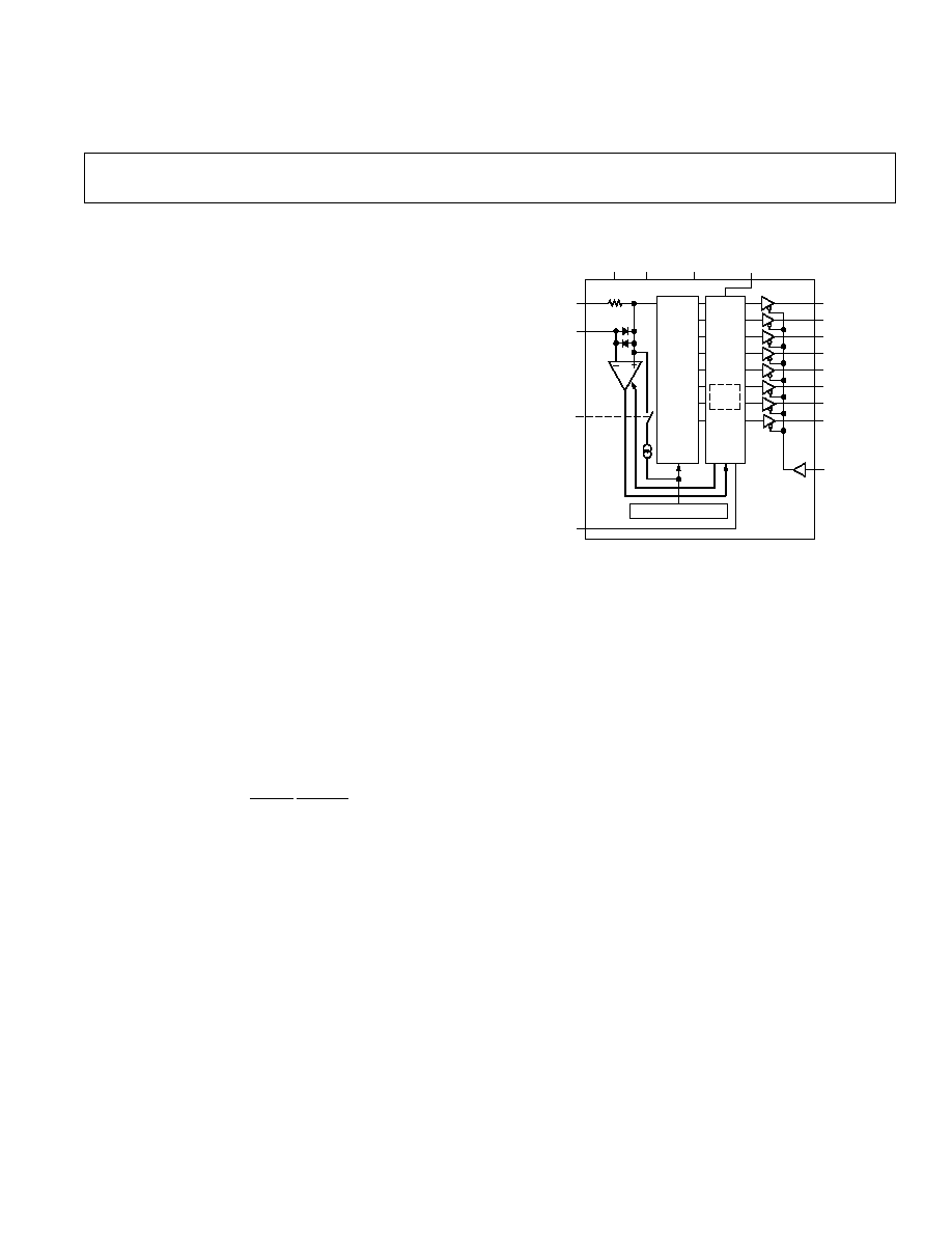
FUNCTIONAL DESCRIPTION
A block diagram of the AD673 is shown in Figure 1. The posi-
tive CONVERT pulse must be at least 500 ns wide. DR goes
high within 1.5
µ
s after the leading edge of the convert pulse in-
dicating that the internal logic has been reset. The negative edge
of the CONVERT pulse initiates the conversion. The internal
8-bit current output DAC is sequenced by the integrated injec-
tion logic (I
2
L) successive approximation register (SAR) from its
most significant bit to least significant bit to provide an output
current which accurately balances the input signal current
through the 5 k
resistor. The comparator determines whether
the addition of each successively weighted bit current causes the
DAC current sum to be greater or less than the input current; if
the sum is more, the bit is turned off. After testing all bits, the
SAR contains a 8-bit binary code which accurately represents
the input signal to within (0.05% of full scale).
BURIED ZENER REF
COMP-
ARATOR
ANALOG
IN
DB7
V+
V
DIGITAL
COMMON
CONVERT
INT
CLOCK
8-BIT
SAR
DB6
DB5
DB4
DB3
DB2
DB1
DB0
MSB
LSB
ANALOG
COMMON
BIPOLAR
OFFSET
CONTROL
DATA
READY
AD673
5k
DATA
ENABLE
8-BIT
CURRENT
OUTPUT
DAC
Figure 1. AD673 Functional Block Diagram
The SAR drives DR low to indicate that the conversion is com-
plete and that the data is available to the output buffers. DATA
ENABLE
can then be activated to enable the 8-bits of data de-
sired. DATA ENABLE should be brought high prior to the next
conversion to place the output buffers in the high impedance state.
The temperature compensated buried Zener reference provides
the primary voltage reference to the DAC and ensures excellent
stability with both time and temperature. The bipolar offset in-
put controls a switch which allows the positive bipolar offset
current (exactly equal to the value of the MSB less 1/2 LSB) to
be injected into the summing (+) node of the comparator to off-
set the DAC output. Thus the nominal 0 V to +10 V unipolar
input range becomes a 5 V to +5 V range. The 5 k
thin-film
input resistor is trimmed so that with a full-scale input signal, an
input current will be generated which exactly matches the DAC
output with all bits on.
UNIPOLAR CONNECTION
The AD673 contains all the active components required to per-
form a complete A/D conversion. Thus, for many applications,
all that is necessary is connection of the power supplies (+5 V
and 12 V to 15 V), the analog input and the convert pulse.
However, there are some features and special connections which
should be considered for achieving optimum performance. The
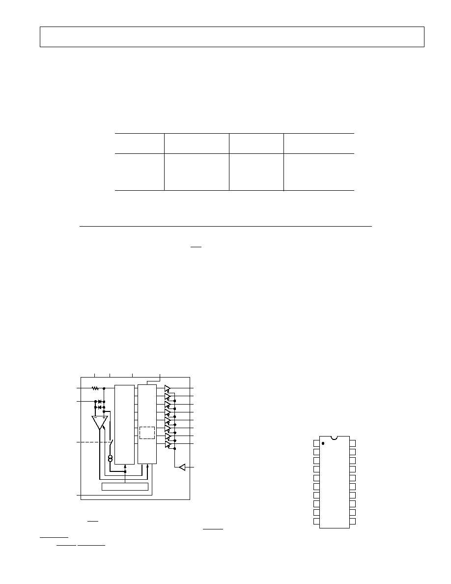
functional pinout is shown in Figure 2.
The standard unipolar 0 V to +10 V range is obtained by short-
ing the bipolar offset control pin (Pin 16) to digital common
(Pin 17).
14
13
12
11
17
16
15
20
19
18
10
9
8
1
2
3
4
7
6
5
TOP VIEW
(Not to Scale)
AD673
*
PINS 1 & 2 ARE INTERNALLY
CONNECTED TO TEST POINTS AND SHOULD BE LEFT FLOATING
NC
*
DIGITAL COMMON
DATA READY
NC
DATA ENABLE
NC
*
LSB DB0
DB1
ANALOG IN
ANALOG COMMON
BIPOLAR OFFSET
DB2
DB3
DB4
DB5
DB6
MSB DB7
V+
CONVERT
V
PIN 1
IDENTIFIER
Figure 2. AD673 Pin Connections
AD673
REV. A
4
Full-Scale Calibration
The 5 k
thin-film input resistor is laser trimmed to produce a
current which matches the full-scale current of the internal
DAC-plus about 0.3%--when an analog input voltage of 9.961
volts (10 volts 1 LSB) is applied at the input. The input resis-
tor is trimmed in this way so that if a fine trimming potentio-
meter is inserted in series with the input signal, the input
current at the full scale input voltage can be trimmed down to
match the DAC full-scale current as precisely as desired. How-
ever, for many applications the nominal 9.961 volt full scale can
be achieved to sufficient accuracy by simply inserting a 15
re-
sistor in series with the analog input to Pin 14. Typical full-scale
calibration error will then be within
±
2 LSB or
±
0.8%. If
more precise calibration is desired, a 200
trimmer should be
used instead. Set the analog input at 9.961 volts, and set the
trimmer so that the output code is just at the transition between
111111 10 and 11111111. Each LSB will then have a weight of
39.06 mV. If a nominal full scale of 10.24 volts is desired
(which makes the LSB have a weight of exactly 40.0 mV), a
100
resistor and a 100
trimmer (or a 200
trimmer with
good resolution) should be used. Of course, larger full-scale
ranges can be arranged by using a larger input resistor, but lin-
earity and full-scale temperature coefficient may be compro-
mised if the external resistor becomes a sizeable percentage of
5 k
Figure 3 illustrates the connections required for full-scale
calibration.
Figure 3. Standard AD673 Connections
Unipolar Offset Calibration
Since the Unipolar Offset is less than
±
1/2 LSB for all versions
of the AD673, most applications will not require trimming. Fig-
ure 4 illustrates two trimming methods which can be used if
greater accuracy is necessary.
Figure 4a shows how the converter zero may be offset to correct
for initial offset and/or input signal offsets. As shown, the circuit
gives approximately symmetrical adjustment in unipolar mode.
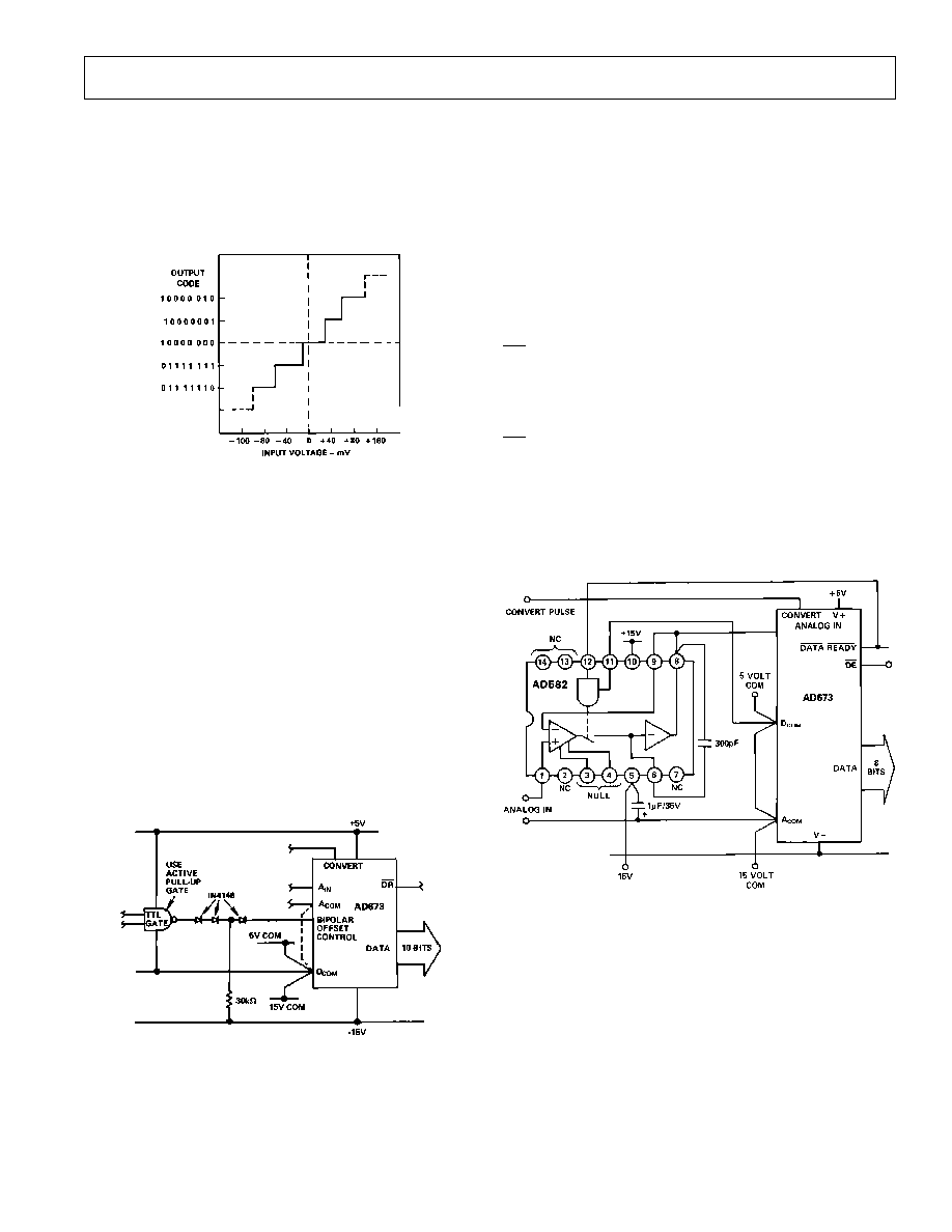
Figure 5 shows the nominal transfer curve near zero for an
AD673 in unipolar mode. The code transitions are at the edges
of the nominal bit weights. In some applications it will be prefer-
able to offset the code transitions so that they fall between the
nominal bit weights, as shown in the offset characteristics.
Figure 5. AD673 Transfer Curve--Unipolar Operation
(Approximate Bit Weights Shown for Illustration,
Nominal Bit Weights % 39.06 mV)
This offset can easily be accomplished as shown in Figure 4b. At
balance (after a conversion) approximately 2 mA flows into the
Analog Common terminal. A 10
resistor in series with this
terminal will result in approximately the desired l/2 bit offset of
the transfer characteristics. The nominal 2 mA Analog Common
current is not closely controlled in manufacture. If high accuracy
is required, a 20
potentiometer (connected as a rheostat) can
be used as R1. Additional negative offset range may be obtained
by using larger values of R1. Of course, if the zero transition
point is changed, the full-scale transition point will also move.
Thus, if an offset of 1/2 LSB is introduced, full scale trimming
as described on the previous page should be done with an analog
input of 9.941 volts.
NOTE: During a conversion, transient currents from the Analog
Common terminal will disturb the offset voltage. Capacitive
decoupling should not be used around the offset network. These
transients will settle appropriately during a conversion. Capaci-
tive decoupling will "pump up" and fail to settle resulting in
conversion errors. Power supply decoupling, which returns to
analog signal common, should go to the signal input side of the
resistive offset network.
Figure 4. Unipolar Offset Trimming
Figure 4a.
Figure 4b.
AD673
REV. A
5
BIPOLAR CONNECTION
To obtain the bipolar 5 V to +5 V range with an offset binary
output code, the bipolar offset control pin is left open.
A 5.00 volt signal will give a 8-bit code of 00000000; an input
of 0.00 volts results in an output code of 10000000 and +4.961
volts at the input yields the 11111111 code. The nominal trans-
fer curve is shown in Figure 6.
Figure 6. AD673 Transfer Curve--Bipolar Operation
Note that in the bipolar mode, the code transitions are offset
1/4 LSB such that an input voltage of 0 volts 5 mV to +35 mV
yields the code representing zero (10000000). Each output code
is then centered on its nominal input voltage.
Full-Scale Calibration
Full-Scale Calibration is accomplished in the same manner as in
Unipolar operation except the full-scale input voltage is +4.61
volts.
Negative Full-Scale Calibration
The circuit in Figure 4a can also be used in Bipolar operation to
offset the input voltage (nominally 5 V) which results in the
000000 00 code. R2 should be omitted to obtain a symmetrical
range.
The bipolar offset control input is not directly TTL compatible
but a TTL interface for logic control can be constructed as
shown in Figure 7.
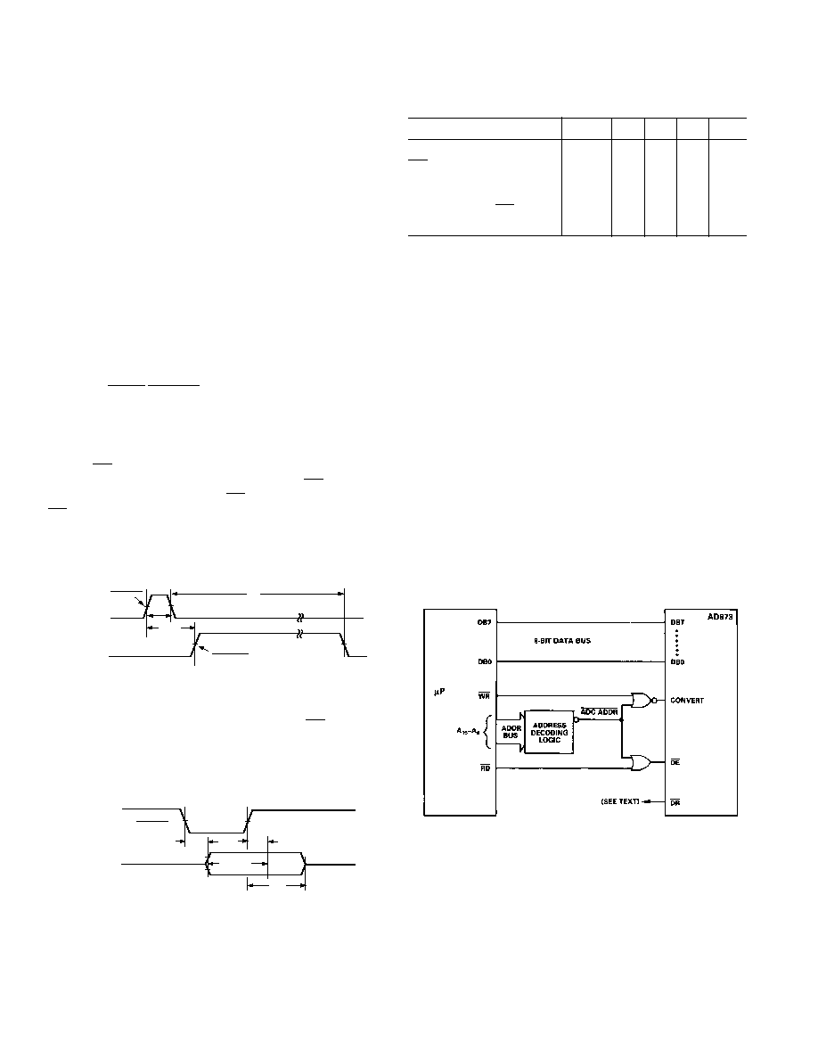
Figure 7. Bipolar Offset Controlled by Logic Gate
Gate Output = 1 Unipolar 0 V10 V Input Range
Gate Output = 0 Bipolar
±
5 V Input Range
SAMPLE-HOLD AMPLIFIER CONNECTION
TO THE AD673
Many situations in high-speed acquisition systems or digitizing
rapidly changing signals require a sample-hold amplifier (SHA)
in front of the A-D converter. The SHA can acquire and hold a
signal faster than the converter can perform a conversion. A
SHA can also be used to accurately define the exact point in
time at which the signal is sampled. For the AD673, a SHA can
also serve as a high input impedance buffer.
Figure 8 shows the AD673 connected to the AD582 monolithic
SHA for high speed signal acquisition. In this configuration, the
AD582 will acquire a 10 volt signal in less than 10
µ
s with a
droop rate less than 100
µ
V/ms.
DR
goes high after the conversion is initiated to indicate that re-
set of the SAR is complete. In Figure 8 it is also used to put the
AD582 into the hold mode while the AD673 begins its conver-
sion cycle. (The AD582 settles to final value well in advance of
the first comparator decision inside the AD673).
DR
goes low when the conversion is complete placing the
AD582 back in the sample mode. Configured as shown in Fig-
ure 8, the next conversion can be initiated after a 10
µ
s delay to
allow for signal acquisition by the AD582.
Observe carefully the ground, supply, and bypass capacitor con-
nections between the two devices. This will minimize ground
noise and interference during the conversion cycle.
Figure 8. Sample-Hold Interface to the AD673
AD673
REV. A
6
GROUNDING CONSIDERATIONS
The AD673 provides separate Analog and Digital Common
connections. The circuit will operate properly with as much as
±
200 mV of common-mode voltage between the two commons.
This permits more flexible control of system common bussing
and digital and analog returns.
In normal operation, the Analog Common terminal may gener-
ate transient currents of up to 2 mA during a conversion. In ad-
dition a static current of about 2 mA will flow into Analog
Common in the unipolar mode after a conversion is complete.
The Analog Common current will be modulated by the varia-
tions in input signal.
The absolute maximum voltage rating between the two com-
mons is
±
1 volt. It is recommended that a parallel pair of
back-to-back protection diodes be connected between the
commons if they are not connected locally.
CONTROL AND TIMING OF THE AD673
The operation of the AD673 is controlled by two inputs: CON-
VERT and DATA ENABLE.
Starting a Conversion
The conversion cycle is initiated by a positive-going CONVERT
pulse at least 500 ns wide. The rising edge of this pulse resets
the internal logic, clears the result of the previous conversion,
and sets DR high. The falling edge of CONVERT begins the
conversion cycle. When conversion is completed DR returns
low. During the conversion cycle, DE should be held high. If
DE
goes low during a conversion, the data output buffers will be
enabled and intermediate conversion results will be present on
the data output pins. This may cause bus conflicts if other de-
vices in a system are trying to use the bus.
t
CS
t
DSC
V
OH
+ V
OL
2
V
IH
+ V
IL
2
t
C
CONVERT
DR
Figure 9. Convert Timing
Reading the Data
The three-state data output buffers is enabled by DE. Access
time of these buffers is typically 150 ns (250 maximum). The
Data outputs remain valid until 50 ns after the enable signal re-
turns high, and are completely into the high-impedance state
100 ns later.
V
IH
+ V
IL
2
DE
t
HD
t
DD
V
OH
V
OL
DATA
VALID
t
HL
HIGH
IMPEDANCE
HIGH
IMPEDANCE
DB0DB7
Figure 10. Read Timing
TIMING SPECIFICATIONS
Parameter
Symbol Min Typ Max Units
CONVERT Pulse Width
t
CS
500 --
--
ns
DR
Delay from CONVERT t
DSC
--
1
1.5
µ
s
Conversion Time
t
C
10
20
30
µ
s
Data Access Time
t
DD
0
150
250
ns
Data Valid after DE High
t
HD
50
--
--
ns
Output Float Delay
t
HL
--
100
200
ns
MICROPROCESSOR INTERFACE CONSIDERATIONS--
GENERAL
When an analog-to-digital converter like the AD673 is inter-
faced to a microprocessor, several details of the interface must
be considered. First, a signal to start the converter must be gen-
erated; then an appropriate delay period must be allowed to pass
before valid conversion data may be read. In most applications,
the AD673 can interface to a microprocessor system with little
or no external logic.
The most popular control signal configuration consists of de-
coding the address assigned to the AD673, then gating this sig-
nal with the system's WR signal to generate the CONVERT
pulse, and gating it with RD to enable the output buffers. The
use of a memory address and memory WR and RD signals de-
notes "memory-mapped" I/O interfacing, while the use of a
separate I/O address space denotes "isolated I/O" interfacing.
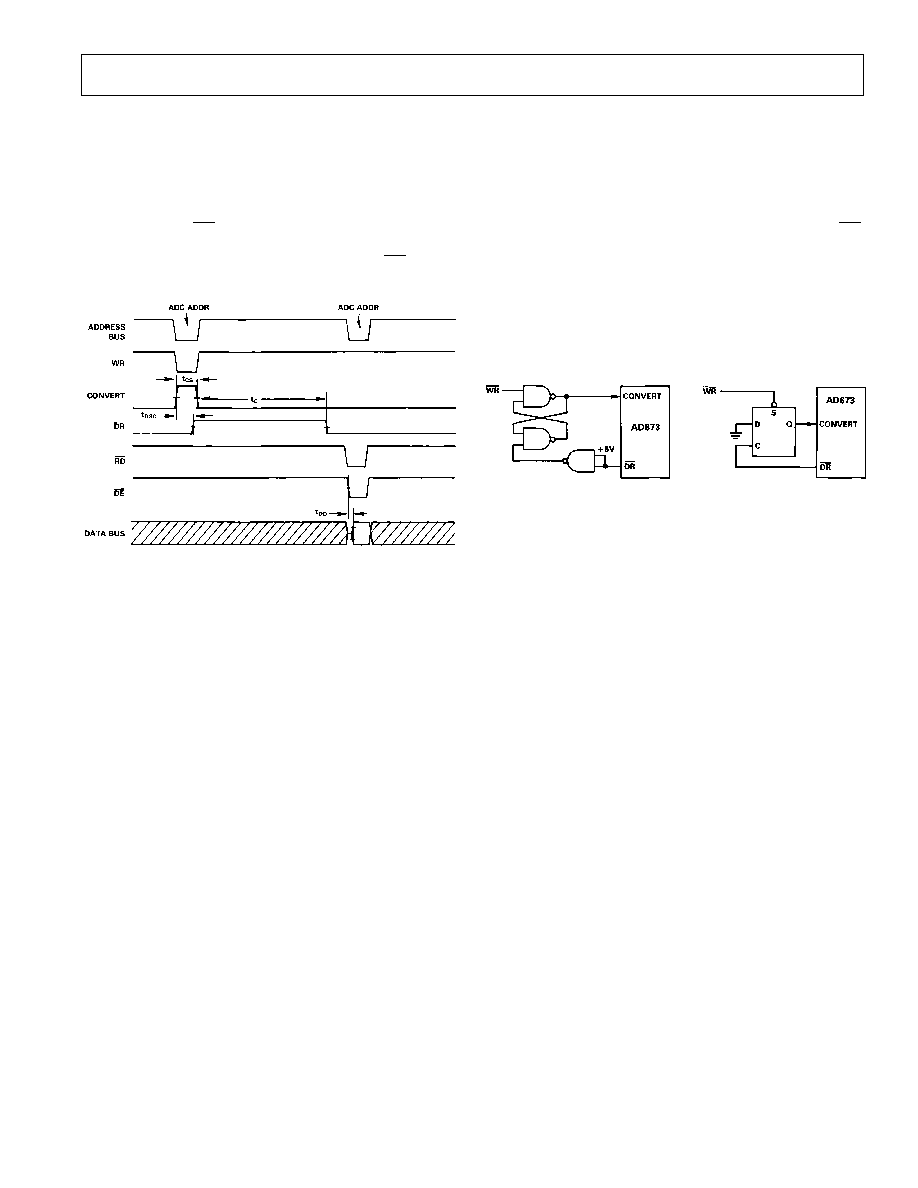
Figure 11 shows a generalized diagram of the control logic for
an AD673 interfaced to an 8-bit data bus, where an address
ADC ADDR has been decoded. ADC ADDR starts the con-
verter when written to (the actual data being written to the con-
verter does not matter) and contains the high byte data during
read operations.
Figure 11. General AD673 Interface to 8-Bit
Microprocessor
AD673
REV. A
7
In systems where this read-write interface is used, at least
30 microseconds (the maximum conversion time) must be al-
lowed to pass between starting a conversion and reading the re-
sults. This delay or "time-out" period can be implemented in a
short software routine such as a countdown loop, enough
dummy instructions to consume 30 microseconds, or enough
actual useful instructions to consume the required time. In tightly-
timed systems, the DR line may be read through an external
three-state buffer to determine precisely when a conversion is
complete. Higher-speed systems may choose to use DR to signal
an interrupt to the processor at the end of a conversion.
Figure 12. Typical AD673 Timing Diagram
CONVERT Pulse Generation
The AD673 is tested with a CONVERT pulse width of 500 ns
and will typically operate with a pulse as short as 300 ns. How-
ever, some microprocessors produce active WR pulses which are
shorter than this. Either of the circuits shown in Figure 13 can
be used to generate an adequate CONVERT pulse for the
AD673. In both circuits, the short low-going WR pulse sets the
CONVERT line high through a flip-flop. The rising edge of DR
(which signifies that the internal logic has been reset) resets
the flip-flop and brings CONVERT low, which starts the
conversion.
Note that t
DSC
is slightly longer when the result of the previous
conversion contains a Logic 1 on the LSB. This means that the
actual CONVERT pulse generated by the circuits in Figure 13
will vary slightly in width.
Figure 13a. Using 74LS00
Figure 13b. Using 1/2 74LS74
AD673
REV. A
8
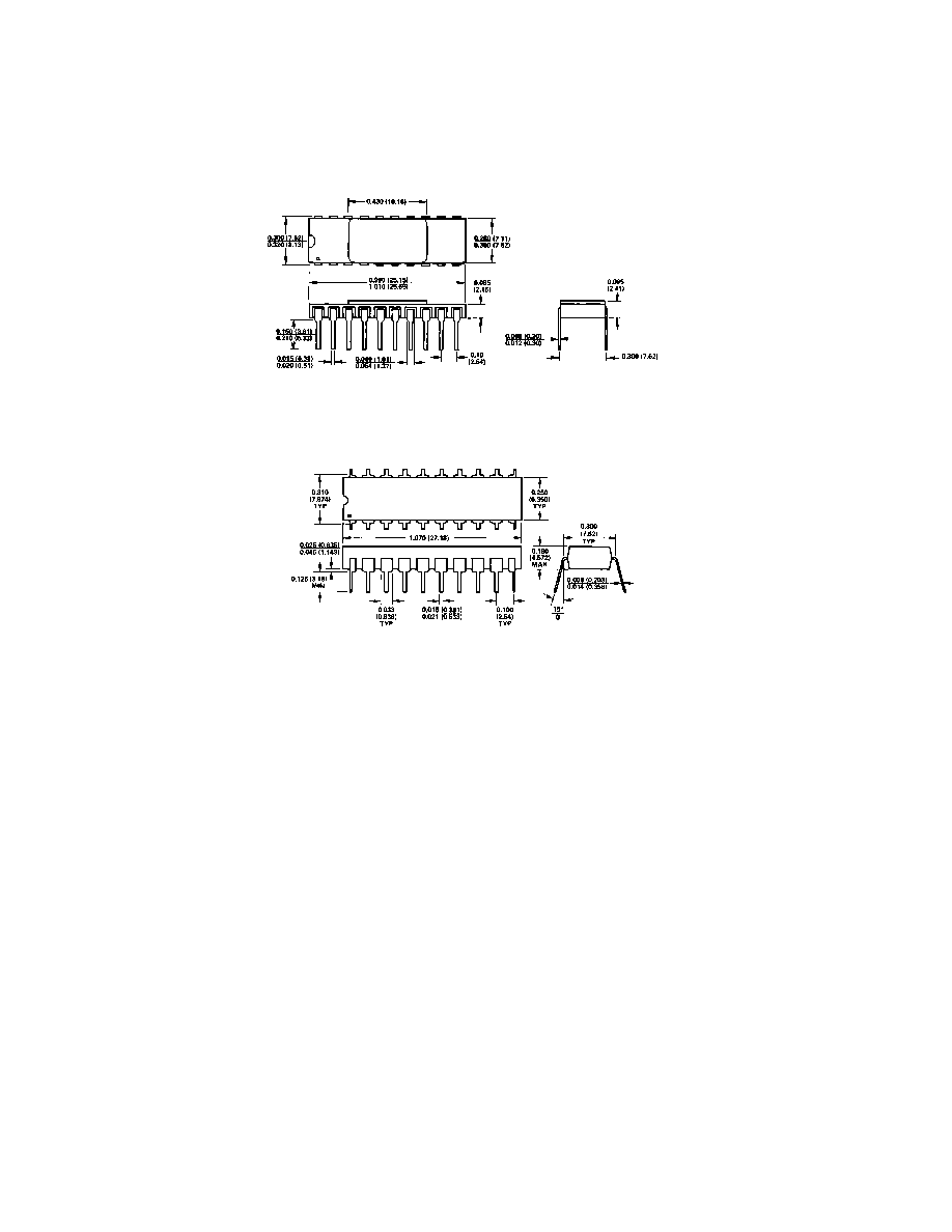
OUTLINE DIMENSIONS
Dimensions shown in inches and (mm).
20-Pin Ceramic DIP (D-20)
20-Pin Plastic DIP (N-20)
C853c53/87
PRINTED IN U.S.A.