 | ÐлекÑÑоннÑй компоненÑ: AD676BD | СкаÑаÑÑ:  PDF PDF  ZIP ZIP |
Äîêóìåíòàöèÿ è îïèñàíèÿ www.docs.chipfind.ru
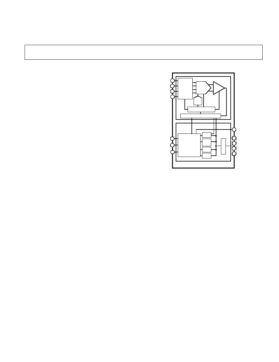
FUNCTIONAL BLOCK DIAGRAM
DIGITAL
CHIP
PAT
GEN
ALU
RAM
MICRO-CODED
CONTROLLER
AGND
AGND SENSE
CAL
SAMPLE
BUSY
COMP
ANALOG
CHIP
16-BIT
DAC
INPUT
BUFFERS
LOGIC & TIMING
CAL
DAC
LEVEL TRANSLATORS
16
BIT 1 BIT 16
V
IN
V
REF
15
14
16
13
8
9
AD676
SAR
1
6
19
28
CLK 10
L
A
T
C
H
7
REV. A
Information furnished by Analog Devices is believed to be accurate and
reliable. However, no responsibility is assumed by Analog Devices for its
use, nor for any infringements of patents or other rights of third parties
which may result from its use. No license is granted by implication or
otherwise under any patent or patent rights of Analog Devices.
a
16-Bit 100 kSPS
Sampling ADC
AD676
FEATURES
Autocalibrating
On-Chip Sample-Hold Function
Parallel Output Format
16 Bits No Missing Codes
1 LSB INL
97 dB THD
90 dB S/(N+D)
1 MHz Full Power Bandwidth
PRODUCT DESCRIPTION
The AD676 is a multipurpose 16-bit parallel output analog-to-
digital converter which utilizes a switched-capacitor/charge
redistribution architecture to achieve a 100 kSPS conversion
rate (10
µ
s total conversion time). Overall performance is opti-
mized by digitally correcting internal nonlinearities through
on-chip autocalibration.
The AD676 circuitry is segmented onto two monolithic chips--
a digital control chip fabricated on Analog Devices DSP CMOS
process and an analog ADC chip fabricated on our BiMOS II
process. Both chips are contained in a single package.
The AD676 is specified for ac (or "dynamic") parameters such
as S/(N+D) Ratio, THD and IMD which are important in sig-
nal processing applications. In addition, dc parameters are
specified which are important in measurement applications.
One Technology Way, P.O. Box 9106, Norwood, MA 02062-9106, U.S.A.
Tel: 617/329-4700
Fax: 617/326-8703
The AD676 operates from +5 V and
±
12 V supplies and typi-
cally consumes 360 mW during conversion. The digital supply
(V
DD
) is separated from the analog supplies (V
CC
, V
EE
) for re-
duced digital crosstalk. An analog ground sense is provided for
the analog input. Separate analog and digital grounds are also
provided.
The AD676 is available in a 28-pin plastic DIP or 28-pin side-
brazed ceramic package. A serial-output version, the AD677, is
available in a 16-pin 300 mil wide ceramic or plastic package.

AD676SPECIFICATIONS
AC SPECIFICATIONS
AD676J/A
AD676K/B
Parameter
Min
Typ
Max
Min
Typ
Max
Units
Total Harmonic Distortion (THD)
2
@ 83 kSPS, T
MIN
to T
MAX
96
88
97
90
dB
0.0016
0.004
0.0014
0.003
%
@ 100 kSPS, +25
°
C
96
97
dB
0.0016
0.0014
%
@ 100 kSPS, T
MIN
to T
MAX
92
92
dB
0.0025
0.0025
%
Signal-to-Noise and Distortion Ratio (S/(N+D))
2, 3
@ 83 kSPS, T
MIN
to T
MAX
85
89
87
90
dB
@ 100 kSPS, +25
°
C
89
90
dB
@ 100 kSPS, T
MIN
to T
MAX
86
86
dB
Peak Spurious or Peak Harmonic Component
98
98
dB
Intermodulation Distortion (IMD)
4
2nd Order Products
102
102
dB
3rd Order Products
98
98
dB
Full Power Bandwidth
1
1
MHz
Noise
160
160
µ
V rms
DIGITAL SPECIFICATIONS
Parameter
Test Conditions
Min
Typ
Max
Units
LOGIC INPUTS
V
IH
High Level Input Voltage
2.4
V
DD
+ 0.3
V
V
IL
Low Level Input Voltage
0.3
0.8
V
I
IH
High Level Input Current
V
IH
= V
DD
10
+10
µ
A
I
IL
Low Level Input Current
V
IL
= 0 V
10
+10
µ
A
C
IN
Input Capacitance
10
pF
LOGIC OUTPUTS
V
OH
High Level Output Voltage
I
OH
= 0.1 mA
V
DD
1 V
V
I
OH
= 0.5 mA
2.4
V
V
OL
Low Level Output Voltage
I
OL
= 1.6 mA
0.4
V
NOTES
1
V
REF
= 10.0 V, (Conversion Rate (fs) = 83 kSPS, f
IN
= 1.0 kHz, V
IN
= 0.05 dB, Bandwidth = fs/2 unless otherwise indicated. All measurements referred to a 0 dB
(20 V p-p) input signal. Values are post-calibration.
2
For other input amplitudes, refer to Figure 13.
3
For other input ranges/voltages reference values see Figure 12.
4
fa = 1008 Hz. fb = 1055 Hz. See Definition of Specifications section and Figure 15.
Specifications subject to change without notice.
(T
MIN
to T
MAX,
V
CC
= +12 V 5%, V
EE
= 12 V 5%, V
DD
= +5 V 10%)
1
(for all grades T
MIN
to T
MAX
, V
CC
= +12 V 5%, V
EE
= 12 V 5%, V
DD
= +5 V 10%)
REV. A
2

DC SPECIFICATIONS
AD676J/A
AD676K/B
Parameter
Min
Typ
Max
Min
Typ
Max
Units
TEMPERATURE RANGE
J, K Grades
0
+70
0
+70
°
C
A, B Grades
40
+85
40
+85
°
C
ACCURACY
Resolution
16
16
Bits
Integral Nonlinearity (INL)
@ 83 kSPS, T
MIN
to T
MAX
±
1
±
1
±
1.5
LSB
@ 100 kSPS, +25
°
C
±
1
±
1
LSB
@ 100 kSPS, T
MIN
to T
MAX
±
2
±
2
LSB
Differential Nonlinearity (DNL)No Missing Codes
16
16
Bits
Bipolar Zero Error
2
(at Nominal Supplies)
0.005
0.005
% FSR
Gain Error (at Nominal Supplies)
@ 83 kSPS
2
0.005
0.005
% FSR
@ 100 kSPS, +25
°
C
0.005
0.005
% FSR
@ 100 kSPS
2
0.01
0.01
% FSR
Temperature Drift, Bipolar Zero
3
% FSR
J, K Grades
0.0015
0.0015
% FSR
A, B Grades
0.003
0.003
% FSR
Temperature Drift, Gain
3
J, K Grades
0.0015
0.0015
% FSR
A, B Grades
0.003
0.003
% FSR
VOLTAGE REFERENCE INPUT RANGE
4
(V
REF
)
5
10
5
10
V
ANALOG INPUT
5
Input Range (V
IN
)
±
V
REF
±
V
REF
V
Input Impedance
*
*
Input Settling Time
2
2
µ
s
Input Capacitance During Sample
50*
50*
pF
Aperture Delay
6
6
ns
Aperture Jitter
100
100
ps
POWER SUPPLIES
Power Supply Rejection
V
CC
= +12 V
±
5%
±
1
±
1
LSB
V
EE
= 12 V
±
5%
±
1
±
1
LSB
V
DD
= +5 V
±
10%
±
1
±
1
LSB
Operating Current
I
CC
14.5
18
14.5
18
mA
I
EE
14.5
18
14.5
18
mA
I
DD
2
5
2
5
mA
Power Consumption
360
480
360
480
mW
NOTES
1
V
REF
= 5.0 V, Conversion Rate = 83 kSPS unless otherwise noted. Values are post-calibration.
2
Values shown apply to any temperature from T
MIN
to T
MAX
after calibration at that temperature.
3
Values shown are based upon calibration at +25
°
C with no additional calibration at temperature. Values shown are the worst case variation from the value at +25
°
C.
4
See "APPLICATIONS" section for recommended voltage reference circuit, and Figure 12 for dynamic performance with other reference voltage values.
5
See "APPLICATIONS" section for recommended input buffer circuit.
*For explanation of input characteristics, see "ANALOG INPUT" section.
Specifications subject to change without notice.
(T
MIN
to T
MAX
, V
CC
= +12 V 5%, V
EE
= 12 V 5%, V
DD
= +5 V 1O%)
1
AD676
REV. A
3
AD676
REV. A
4
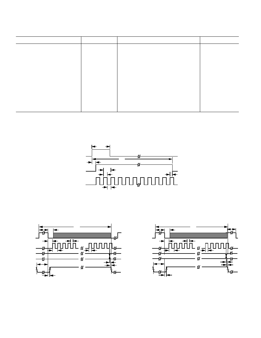
TIMING SPECIFICATIONS
Parameter
Symbol
Min
Typ
Max
Units
Conversion Time
2
t
C
10
1000
µ
s
CLK Period
3
t
CLK
480
ns
Calibration Time
t
CT
85,530
t
CLK
Sampling Time (Included in t
C
)
t
S
2
µ
s
CAL to BUSY Delay
t
CALB
75
150
ns
BUSY to SAMPLE Delay
t
BS
2
µ
s
SAMPLE to BUSY Delay
t
SB
15
100
ns
CLK HIGH
4
t
CH
50
ns
CLK LOW
4
t
CL
50
ns
SAMPLE LOW to 1st CLK Delay
t
SC
50
ns
SAMPLE LOW
t
SL
100
ns
Output Delay
t
OD
125
200
ns
Status Delay
t
SD
50
ns
CAL HIGH Time
t
CALH
50
ns
NOTES
1
See the "CONVERSION CONTROL" and "AUTOCALIBRATION" sections for detailed explanations of the above timing.
2
Depends upon external clock frequency; includes acquisition time and conversion time. The maximum conversion time is specified to account for the droop of the
internal sample/hold function. Longer conversion times may degrade performance. See "General Conversion Guidelines" for additional explanation of maximum con-
version time.
3
580 ns is recommended for optimal accuracy over temperature.
4
t
CH
+ t
CL
= t
CLK
and must be greater than 480 ns.
CAL
BUSY
CLK
t
CH
t
CL
t
CLK
t
CALB
t
OD
t
CT
CALH
t
Figure 1. Calibration Timing
SAMPLE
(INPUT)
CLK
(INPUT)
BIT 1 BIT 16
(OUTPUTS)
BUSY
(OUTPUT)
1
2
3
4
5
t
S
t
SL
t
SC
t
CLK
t
CL
t
CH
t
OD
t
SD
t
SB
t
BS
t
C
13
14
15
16
17
(PREVIOUS CONVERSION)
(NEW DATA)
Figure 2a. General Conversion Timing
SAMPLE
(INPUT)
CLK
(INPUT)
BIT 1 BIT 16
(OUTPUTS)
BUSY
(OUTPUT)
1
2
3
4
5
t
S
t
SL
t
SC
t
CLK
t
CL
t
CH
t
OD
t
SD
t
SB
t
BS
t
C
13
14
15
16
17
t
S
(PREVIOUS CONVERSION)
(NEW DATA)
Figure 2b. Continuous Conversion Timing
(T
MIN
to T
MAX
V
CC
= +12 V 5%, V
EE
= 12 V 5%, V
DD
= +5 V 10%, V
REF
= 10.0 V)
1

AD676
REV. A
5
ORDERING GUIDE
Package
Model
Temperature Range
1
S/(N+D)
Max INL
Package Description
Option
2
AD676JD
0
°
C to +70
°
C
85 dB
Ceramic 28-Pin DIP
D-28
AD676KD
0
°
C to +70
°
C
87 dB
±
1.5 LSB
Ceramic 28-Pin DIP
D-28
AD676AD
40
°
C to +85
°
C
85 dB
Ceramic 28-Pin DIP
D-28
AD676BD
40
°
C to +85
°
C
87 dB
±
1.5 LSB
Ceramic 28-Pin DIP
D-28
NOTES
1
For details on grade and package offerings screened in accordance with MIL-STD-883, refer to the AD676/883 data sheet.
2
D = Ceramic DIP.
ABSOLUTE MAXIMUM RATINGS*
V
CC
to V
EE
. . . . . . . . . . . . . . . . . . . . . . . . . . 0.3 V to +26.4 V
V
DD
to DGND . . . . . . . . . . . . . . . . . . . . . . . . . 0.3 V to +7 V
V
CC
to AGND . . . . . . . . . . . . . . . . . . . . . . . . 0.3 V to +18 V
V
EE
to AGND . . . . . . . . . . . . . . . . . . . . . . . . 18 V to +0.3 V
AGND to DGND . . . . . . . . . . . . . . . . . . . . . . . . . . . .
±
0.3 V
Digital Inputs to DGND . . . . . . . . . . . . . . . . . . 0 V to +5.5 V
Analog Inputs, V
REF
to AGND
. . . . . . . . . . . . . . . . . . . . . . . (V
CC
+ 0.3 V) to (V
EE
0.3 V)
Soldering . . . . . . . . . . . . . . . . . . . . . . . . . . . . . +300
°
C, 10 sec
Storage Temperature . . . . . . . . . . . . . . . . . . 65
°
C to +150
°
C
*Stresses greater than those listed under "Absolute Maximum Ratings" may cause
permanent damage to the device. This is a stress rating only and functional
operation of the device at these or any other conditions above those indicated in
the operational section of this specification is not implied. Exposure to absolute
maximum rating conditions for extended periods may affect device reliability.
WARNING!
ESD SENSITIVE DEVICE
CAUTION
The AD676 features input protection circuitry consisting of large "distributed" diodes and
polysilicon series resistors to dissipate both high energy discharges (Human Body Model) and fast,
low energy pulses (Charged Device Model). Per Method 3015.2 of MIL-STD-883C, the AD676
has been classified as a Category 1 Device.
Proper ESD precautions are strongly recommended to avoid functional damage or performance
degradation. Charges as high as 4000 volts readily accumulate on the human body and test
equipment, and discharge without detection. Unused devices must be stored in conductive foam
or shunts, and the foam discharged to the destination socket before devices are removed. For further
information on ESD Precaution. Refer to Analog Devices' ESD Prevention Manual.
AD676
REV. A
6
PIN DESCRIPTION
Pin
Name
Type
Description
16
BIT 11-BIT 16
DO
BIT 11BIT 16 represent the six LSBs of data.
7
BUSY
DO
Status Line for Converter. Active HIGH, indicating a conversion or calibration in progress.
BUSY should be buffered when capacitively loaded.
8
CAL
DI
Calibration Control Pin (Asynchronous).
9
SAMPLE
DI
V
IN
Acquisition Control Pin. Active HIGH. During conversion, SAMPLE controls the state
of the internal sample-hold amplifier and the falling edge initiates conversion (see "Conver-
sion Control" paragraph). During calibration, SAMPLE should be held LOW. If HIGH dur-
ing calibration, diagnostic information will appear on the two LSBs (Pins 5 and 6).
10
CLK
DI
Master Clock Input. The AD676 requires 17 clock cycles to execute a conversion.
11
DGND
P
Digital Ground.
12
V
CC
P
+12 V Analog Supply Voltage.
13
AGND
P/AI
Analog Ground.
14
AGND SENSE
AI
Analog Ground Sense.
15
V
IN
AI
Analog Input Voltage.
16
V
REF
AI
External Voltage Reference Input.
17
V
EE
P
12 V Analog Supply Voltage. Note: the lid of the ceramic package is internally connected to
V
EE
.
18
V
DD
P
+5 V Logic Supply Voltage.
1928
BIT 1BIT 10
DO
BIT 1BIT 10 represent the ten MSB of data.
Type: AI = Analog Input
DI = Digital Input
DO = Digital Output
P = Power
1
2
3
4
5
6
7
8
9
10
11
12
13
14
28
27
26
25
24
23
22
21
20
19
18
17
16
15
TOP VIEW
(Not to Scale)
AD676
BIT 10
BIT 9
BIT 8
BIT 7
BIT 6
BIT 5
BIT 4
BIT 3
BIT 2
BIT 1 (MSB)
V
DD
V
EE
V
REF
V
IN
BIT 11
BIT 12
BIT 13
BIT 14
BIT 15
BIT 16 (LSB)
BUSY
CAL
SAMPLE
CLK
DGND
V
CC
AGND
AGND SENSE
Package Pinout
DIGITAL
CHIP
PAT
GEN
ALU
RAM
MICRO-CODED
CONTROLLER
AGND
AGND SENSE
CAL
SAMPLE
BUSY
COMP
ANALOG
CHIP
16-BIT
DAC
INPUT
BUFFERS
LOGIC & TIMING
CAL
DAC
LEVEL TRANSLATORS
16
BIT 1 BIT 16
V
IN
V
REF
15
14
16
13
8
9
AD676
SAR
1
6
19
28
CLK 10
L
A
T
C
H
7
Functional Block Diagram

AD676
REV. A
7
NYQUIST FREQUENCY
An implication of the Nyquist sampling theorem, the "Nyquist
frequency" of a converter is that input frequency which is one
half the sampling frequency of the converter.
TOTAL HARMONIC DISTORTION
Total harmonic distortion (THD) is the ratio of the rms sum of
the harmonic components to the rms value of a full-scale input
signal and is expressed in percent (%) or decibels (dB). For in-
put signals or harmonics that are above the Nyquist frequency,
the aliased components are used.
SIGNAL-TO-NOISE PLUS DISTORTION RATIO
Signal-to-noise plus distortion is defined to be the ratio of the
rms value of the measured input signal to the rms sum of all
other spectral components below the Nyquist frequency, includ-
ing harmonics but excluding dc.
GAIN ERROR
The last transition should occur at an analog value 1.5 LSB be-
low the nominal full scale (4.99977 volts for a
±
5 V range). The
gain error is the deviation of the actual difference between the
first and last code transition from the ideal difference between
the first and last code transition.
BIPOLAR ZERO ERROR
Bipolar zero error is the difference between the ideal midscale
input voltage (0 V) and the actual voltage producing the
midscale output code.
DIFFERENTIAL NONLINEARITY (DNL)
In an ideal ADC, code transitions are one LSB apart. Differen-
tial nonlinearity is the maximum deviation from this ideal value.
It is often specified in terms of resolution for which no missing
codes are guaranteed.
INTEGRAL NONLINEARITY (INL)
The ideal transfer function for an ADC is a straight line bisect-
ing the center of each code drawn between "zero" and "full
scale." The point used as "zero" occurs 1/2 LSB before the
most negative code transition. "Full scale" is defined as a level
1.5 LSB beyond the most positive code transition. Integral
nonlinearity is the worst-case deviation of a code center average
from the straight line.
BANDWIDTH
The full-power bandwidth is that input frequency at which the
amplitude of the reconstructed fundamental is reduced by 3 dB
for a full-scale input.
INTERMODULATION DISTORTION (IMD)
With inputs consisting of sine waves at two frequencies, fa and
fb, any device with nonlinearities will create distortion products,
of order (m+n), at sum and difference frequencies of mfa
±
nfb,
where m, n = 0, 1, 2, 3. . . . Intermodulation terms are those for
which m or n is not equal to zero. For example, the second or-
der terms are (fa + fb) and (fa fb), and the third order terms
are (2 fa + fb), (2 fa fb), (fa + 2 fb) and (fa 2 fb). The IMD
products are expressed as the decibel ratio of the rms sum of the
measured input signals to the rms sum of the distortion terms.
The two signals applied to the converter are of equal amplitude,
and the peak value of their sum is 0.5 dB from full scale. The
IMD products are normalized to a 0 dB input signal.
APERTURE DELAY
Aperture delay is the time required after SAMPLE pin is taken
LOW for the internal sample-hold of the AD676 to open, thus
holding the value of V
lN
.
APERTURE JITTER
Aperture jitter is the variation in the aperture delay from sample
to sample.
POWER SUPPLY REJECTION
DC variations in the power supply voltage will affect the overall
transfer function of the ADC, resulting in zero error and gain er-
ror changes. Power supply rejection is the maximum change in
either the bipolar zero error or gain error value. Additionally,
there is another power supply variation to consider. AC ripple
on the power supplies can couple noise into the ADC, resulting
in degradation of dynamic performance. This is displayed in
Figure 16.
INPUT SETTLING TIME
Settling time is a function of the SHA's ability to track fast
slewing signals. This is specified as the maximum time required
in track mode after a full-scale step input to guarantee rated
conversion accuracy.
Definition of Specifications

AD676
REV. A
8
FUNCTIONAL DESCRIPTION
The AD676 is a multipurpose 16-bit analog-to-digital converter
and includes circuitry which performs an input sample/hold
function, ground sense, and autocalibration. These functions
are segmented onto two monolithic chips--an analog signal pro-
cessor and a digital controller. Both chips are contained within
the AD676 package.
The AD676 employs a successive-approximation technique to
determine the value of the analog input voltage. However, in-
stead of the traditional laser-trimmed resistor-ladder approach,
this device uses a capacitor-array, charge redistribution tech-
nique. Binary-weighted capacitors subdivide the input sample to
perform the actual analog-to-digital conversion. The capacitor
array eliminates variation in the linearity of the device due to
temperature-induced mismatches of resistor values. Since a ca-
pacitor array is used to perform the data conversions, the
sample/hold function is included without the need for additional
external circuitry.
Initial errors in capacitor matching are eliminated by an auto-
calibration circuit within the AD676. This circuit employs an
on-chip microcontroller and a calibration DAC to measure and
compensate capacitor mismatch errors. As each error is deter-
mined, its value is stored in on-chip memory (RAM). Subse-
quent conversions use these RAM values to improve conversion
accuracy. The autocalibration routine may be invoked at any
time. Autocalibration insures high performance while eliminat-
ing the need for any user adjustments and is described in detail
below.
The microcontroller controls all of the various functions within
the AD676. These include the actual successive approximation
algorithm, the autocalibration routine, the sample/hold opera-
tion, and the internal output data latch.
AUTOCALIBRATION
The AD676 achieves rated performance without the need for
user trims or adjustments. This is accomplished through the use
of on-chip autocalibration.
In the autocalibration sequence, sample/hold offset is nulled by
internally connecting the input circuit to the ground sense cir-
cuit. The resulting offset voltage is measured and stored in
RAM for later use. Next, the capacitor representing the most
significant bit (MSB) is charged to the reference voltage. This
charge is then transferred to a capacitor of equal size (composed
of the sum of the remaining lower weight bits). The difference
in the voltage that results and the reference voltage represents
the amount of capacitor mismatch. A calibration digital-to-ana-
log converter (DAC) adds an appropriate value of error correc-
tion voltage to cancel this mismatch. This correction factor is
also stored in RAM. This process is repeated for each of the
capacitors representing the remaining top eight bits. The accu-
mulated values in RAM are then used during subsequent con-
versions to adjust conversion results accordingly.
As shown in Figure 1, when CAL is taken HIGH the AD676 in-
ternal circuitry is reset, the BUSY pin is driven HIGH, and the
ADC prepares for calibration. This is an asynchronous hard-
ware reset and will interrupt any conversion or calibration cur-
rently in progress. Actual calibration begins when CAL is taken
LOW and completes in 85,530 clock cycles, indicated by BUSY
going LOW. During calibration, it is preferable for SAMPLE to
be held LOW. If SAMPLE is HIGH, diagnostic data will appear
on Pins 5 and 6. This data is of no value to the user.
The AD676 requires one clock cycle after BUSY goes LOW to
complete the calibration cycle. If this clock cycle is not pro-
vided, it will be taken from the first conversion, likely resulting
in first conversion error.
In most applications, it is sufficient to calibrate the AD676 only
upon power-up, in which case care should be taken that the
power supplies and voltage reference have stabilized first. If not
calibrated, the AD676 accuracy may be as low as 10 bits.
CONVERSION CONTROL
The AD676 is controlled by two signals: SAMPLE and CLK, as
shown in Figures 2a and 2b. It is assumed that the part has been
calibrated and the digital I/O pins have the levels shown at the
start of the timing diagram.
A conversion consists of an input acquisition followed by 17
clock pulses which execute the 16-bit internal successive ap-
proximation routine. The analog input is acquired by taking the
SAMPLE line HIGH for a minimum sampling time of t
S
. The
actual sample taken is the voltage present on V
IN
one aperture
delay after the SAMPLE line is brought LOW, assuming the
previous conversion has completed (signified by BUSY going
LOW). Care should he taken to ensure that this negative edge is
well defined and jitter free in ac applications to reduce the un-
certainty (noise) in signal acquisition. With SAMPLE going
LOW, the AD676 commits itself to the conversion--the input at
V
IN
is disconnected from the internal capacitor array, BUSY
goes HIGH, and the SAMPLE input will be ignored until the
conversion is completed (when BUSY goes LOW). SAMPLE
must be held LOW for a minimum period of time t
SL
. A period
of time t
SC
after bringing SAMPLE LOW, the 17 CLK cycles
are applied; CLK pulses that start before this period of time are
ignored. BUSY goes HIGH t
SB
after SAMPLE goes LOW, sig-
nifying that a conversion is in process, and remains HIGH until
the conversion is completed. BUSY goes LOW during the 17th
CLK cycle at the point where the data outputs have changed
and are valid. The AD676 will ignore CLK after BUSY has
gone LOW and the output data will remain constant until a new
conversion is completed. The data can, therefore, be read any
time after BUSY goes LOW and before the 17th CLK of the
next conversion (see Figures 2a and 2b). The section on Micro-
processor Interfacing discusses how the AD676 can be inter-
faced to a 16-bit databus.
Typically BUSY would be used to latch the AD676 output data
into buffers or to interrupt microprocessors or DSPs. It is rec-
ommended that the capacitive load on BUSY be minimized by
driving no more than a single logic input. Higher capacitive
loads such as cables or multiple gates may degrade conversion
quality unless BUSY is buffered.
AD676
REV. A
9
CONTINUOUS CONVERSION
For maximum throughput rate, the AD676 can be operated in a
continuous convert mode (see Figure 2b). This is accomplished
by utilizing the fact that SAMPLE will no longer be ignored af-
ter BUSY goes LOW, so an acquisition may be initiated even
during the HIGH time of the 17th CLK pulse for maximum
throughput rate while enabling full settling of the sample/hold
circuitry. If SAMPLE is already HIGH when BUSY goes LOW
at the end of a conversion, then an acquisition is immediately
initiated and t
S
and t
C
start from that time. Data from the previ-
ous conversion may be latched up to t
SD
before BUSY goes
LOW or t
OD
after the rising edge of the 17th clock pulse. How-
ever, it is preferred that latching occur on or after the falling
edge of BUSY.
Care must he taken to adhere to the minimum/maximum timing
requirements in order to preserve conversion accuracy.
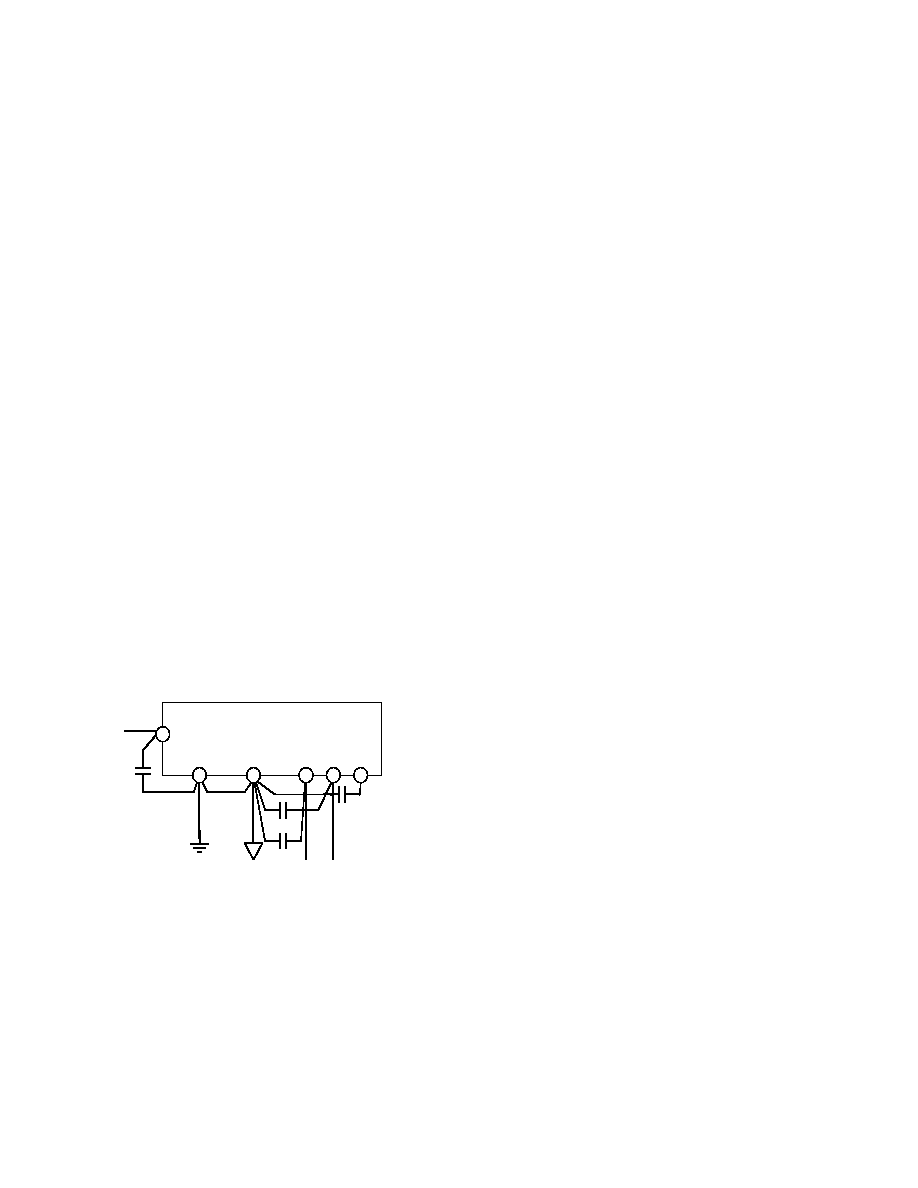
GENERAL CONVERSION GUIDELINES
During signal acquisition and conversion, care should be taken
with the logic inputs to avoid digital feedthrough noise. It is pos-
sible to run CLK continuously, even during the sample period.
However, CLK edges during the sampling period, and especially
when SAMPLE goes LOW, may inject noise into the sampling
process. The AD676 is tested with no CLK cycles during the
sampling period. The BUSY signal can be used to prevent the
clock from running during acquisition, as illustrated in Figure 3.
In this circuit BUSY is used to reset the circuitry which divides
the system clock down to provide the AD676 CLK. This serves
to interrupt the clock until after the input signal has been ac-
quired, which has occurred when BUSY goes HIGH. When the
conversion is completed and BUSY goes LOW, the circuit in
Figure 3 truncates the 17th CLK pulse width which is tolerable
because only its rising edge is critical.
5
2
10
7
1
7
12
9
4
11
12.288MHz
SYSTEM
CLOCK
CLK
74HC175
2D
1Q
CLR
3D
2Q
3Q
1D
BUSY
CLK
AD676
9
SAMPLE
2
8
9
12
6
13
1
1QD
74HC393
1CLR
2CLR
2QD
2QC
1CLK
2CLK
Figure 3.
Figure 3 also illustrates the use of a counter (74HC393) to de-
rive the AD676 SAMPLE command from the system clock
when a continuous convert mode is desirable. Pin 9 (2QC) pro-
vides a 96 kHz sample rate for the AD676 when used with a
12.288 MHz system clock. Alternately, Pin 8 (2QD) could be
used for a 48 kHz rate.
If a continuous clock is used, then the user must avoid CLK
edges at the instant of disconnecting V
IN
which occurs at the
falling edge of SAMPLE (see t
SC
specification). The duty cycle
of CLK may vary, but both the HIGH (t
CH
) and LOW (t
CL
)
phases must conform to those shown in the timing specifica-
tions. The internal comparator makes its decisions on the rising
edge of CLK. To avoid a negative edge transition disturbing the
comparator's settling, t
CL
should be at least half the value of t
CLK
.
To also avoid transitions disturbing the internal comparator's
settling, it is not recommended that the SAMPLE pin change
state toward the end of a CLK cycle.
During a conversion, internal dc error terms such as comparator
voltage offset are sampled, stored on internal capacitors and
used to correct for their corresponding errors when needed. Be-
cause these voltages are stored on capacitors, they are subject to
leakage decay and so require refreshing. For this reason there is
a maximum conversion time t
C
(1000
µ
s). From the time
SAMPLE goes HIGH to the completion of the 17th CLK pulse,
no more than 1000
µ
s should elapse for specified performance.
However, there is no restriction to the maximum time between
conversions.
Output coding for the AD676 is twos complement, as shown in
Table I. By inverting the MSB, the coding can be converted to
offset binary. The AD676 is designed to limit output coding in
the event of out-of-range inputs.
Table I. Output Coding
V
IN
Output Code
>Full Scale
011 . . . 11
Full Scale
011 . . . 11
Full Scale 1 LSB
011 . . . 10
Midscale + 1 LSB
000 . . . 01
Midscale
000 . . . 00
Midscale 1 LSB
111 . . . 11
Full Scale + 1 LSB
100 . . . 01
Full Scale
100 . . . 00
<Full Scale
100 . . . 00
AD676
REV. A
10
POWER SUPPLIES AND DECOUPLING
The AD676 has three power supply input pins. V
CC
and V
EE
provide the supply voltages to operate the analog portions of the
AD676 including the ADC and sample-hold amplifier (SHA).
V
DD
provides the supply voltage which operates the digital por-
tions of the AD676 including the data output buffers and the
autocalibration controller.
As with most high performance linear circuits, changes in the
power supplies can produce undesired changes in the perfor-
mance of the circuit. Optimally, well regulated power supplies
with less than 1% ripple should be selected. The ac output im-
pedance of a power supply is a complex function of frequency,
and in general will increase with frequency. In other words, high
frequency switching such as that encountered with digital cir-
cuitry requires fast transient currents which most power supplies
cannot adequately provide. This results in voltage spikes on the
supplies. If these spikes exceed the
±
5% tolerance of the
±
12 V
supplies or the
±
10% limits of the +5 V supply, ADC perfor-
mance will degrade. Additionally, spikes at frequencies higher
than 100 kHz will also degrade performance. To compensate for
the finite ac output impedance of the supplies, it is necessary to
store "reserves" of charge in bypass capacitors. These capacitors
can effectively lower the ac impedance presented to the AD676
power inputs which in turn will significantly reduce the magni-
tude of the voltage spikes. For bypassing to be effective, certain
guidelines should be followed. Decoupling capacitors, typically
0.1
µ
F, should be placed as closely as possible to each power
supply pin of the AD676. It is essential that these capacitors be
placed physically close to the IC to minimize the inductance of
the PCB trace between the capacitor and the supply pin. The
logic supply (V
DD
) should be decoupled to digital common and
the analog supplies (Vcc and V
EE
) to analog common. The ref-
erence input is also considered as a power supply pin in this re-
gard and the same decoupling procedures apply. These points
are displayed in Figure 4.
+5V
12V 12V
SYSTEM
ANALOG
COMMON
SYSTEM
DIGITAL
COMMON
AGND
DGND
AD676
17
12
13
11
18
EE
V
CC
V
11
V
REF
V
DD
0.1
µ
F
0.1
µ
F
0.1
µ
F
0.1
µ
F
Figure 4. Grounding and Decoupling the AD676
Additionally, it is beneficial to have large capacitors (>47
µ
F)
located at the point where the power connects to the PCB with
10
µ
F capacitors located in the vicinity of the ADC to further
reduce low frequency ripple. In systems that will be subjected to
particularly harsh environmental noise, additional decoupling
may be necessary. RC-filtering on each power supply combined
with dedicated voltage regulation can substantially decrease
power supply ripple effects (this is further detailed in Figure 7).
BOARD LAYOUT
Designing with high resolution data converters requires careful
attention to board layout. Trace impedance is a significant issue.
A 1.22 mA current through a 0.5
trace will develop a voltage
drop of 0.6 mV, which is 4 LSBs at the 16-bit level for a 10 V
full-scale span. In addition to ground drops, inductive and ca-
pacitive coupling need to be considered, especially when high
accuracy analog signals share the same board with digital
signals.
Analog and digital signals should not share a common return
path. Each signal should have an appropriate analog or digital
return routed close to it. Using this approach, signal loops en-
close a small area, minimizing the inductive coupling of noise.
Wide PC tracks, large gauge wire, and ground planes are highly
recommended to provide low impedance signal paths. Separate
analog and digital ground planes are also desirable, with a single
interconnection point at the AD676 to minimize interference
between analog and digital circuitry. Analog signals should be
routed as far as possible from digital signals and should cross
them, if at all, only at right angles. A solid analog ground plane
around the AD676 will isolate it from large switching ground
currents. For these reasons, the use of wire wrap circuit con-
struction will not provide adequate performance; careful printed
circuit board construction is preferred.
GROUNDING
The AD676 has three grounding pins, designated ANALOG
GROUND (AGND), DIGITAL GROUND (DGND) and
ANALOG GROUND SENSE (AGND SENSE). The analog
ground pin is the "high quality" ground reference point for the
device, and should be connected to the analog common point in
the system.
AGND SENSE is intended to be connected to the input signal
ground reference point. This allows for slight differences in level
between the analog ground point in the system and the input
signal ground point. However no more than 100 mV is recom-
mended between the AGND and the AGND SENSE pins for
specified performance.
AD676
REV. A
11
Using AGND SENSE to remotely sense the ground potential of
the signal source can be useful if the signal has to be carried
some distance to the A/D converter. Since all IC ground cur-
rents have to return to the power supply and no ground leads
are free from resistance and inductance, there are always some
voltage differences from one ground point in a system to
another.
Over distance this voltage difference can easily amount to sev-
eral LSBs (in a 10 V input span, 16-bit system each LSB is
about 0.15 mV). This would directly corrupt the A/D input sig-
nal if the A/D measures its input with respect to power ground
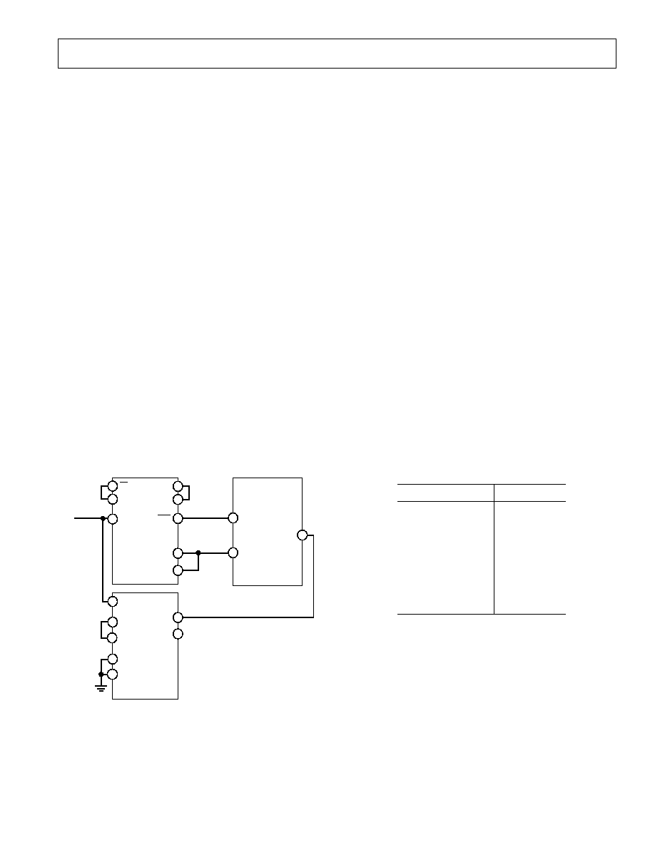
(AGND) as shown in Figure 5a. To solve this problem the
AD676 offers an AGND SENSE pin. Figure 5b shows how the
AGND SENSE can be used to eliminate the problem in Figure
5a. Figure 5b also shows how the signal wires should be
shielded in a noisy environment to avoid capacitive coupling. If
inductive (magnetic) coupling is expected to be dominant such
as where motors are present, twisted-pair wires should be used
instead.
The digital ground pin is the reference point for all of the digital
signals that operate the AD676. This pin should be connected
to the digital common point in the system. As Figure 4 illus-
trated, the analog and digital grounds should be connected to-
gether at one point in the system, preferably at the AD676.
V
IN
AGND
SOURCE
V
S
GROUND LEAD
I
GROUND
> 0
TO POWER
SUPPLY GND
AD676
V
Figure 5a. Input to the A/D Is Corrupted by IR Drop in
Ground Leads: V
IN
= V
S
+
V
V
IN
AGND
SENSE
AGND
SOURCE
V
S
SHIELDED CABLE
GROUND LEAD
I
GROUND
> 0
TO POWER
SUPPLY GND
AD676
Figure 5b. AGND SENSE Eliminates the Problem in
Figure 5a.
VOLTAGE REFERENCE
The AD676 requires the use of an external voltage reference.
The input voltage range is determined by the value of the refer-
ence voltage; in general, a reference voltage of n volts allows an
input range of
±
n volts. The AD676 is specified for both 10 V
and 5.0 V references. A 10 V reference will typically require
support circuitry operated from
±
15 V supplies; a 5.0 V refer-
ence may be used with
±
12 V supplies. Signal-to-noise perfor-
mance is increased proportionately with input signal range. In
the presence of a fixed amount of system noise, increasing the
LSB size (which results from increasing the reference voltage)
will increase the effective S/(N+D) performance. Figure 12
illustrates S/(N+D) as a function of reference voltage. In
contrast, INL will be optimal at lower reference voltage values
(such as 5 V) due to capacitor nonlinearity at higher voltage
values.
During a conversion, the switched capacitor array of the AD676
presents a dynamically changing current load at the voltage ref-
erence as the successive-approximation algorithm cycles through
various choices of capacitor weighting. (See the following sec-
tion "Analog Input" for a detailed discussion of the V
REF
input
characteristics.) The output impedance of the reference circuitry
must be low so that the output voltage will remain sufficiently
constant as the current drive changes. In some applications, this
may require that the output of the voltage reference be buffered
by an amplifier with low impedance at relatively high frequen-
cies. In choosing a voltage reference, consideration should be
made for selecting one with low noise. A capacitor connected
between REF IN and AGND will reduce the demands on the
reference by decreasing the magnitude of high frequency com-
ponents required to be sourced by the reference.
Figures 6 and 7 represent typical design approaches.
V
IN
10
µ
F
AGND
C
N
1.0
µ
F
+12V
AD586
AD676
13
16
6
2
4
8
V
REF
+
Figure 6.
Figure 6 shows a voltage reference circuit featuring the 5 V out-
put AD586. The AD586 is a low cost reference which utilizes a
buried Zener architecture to provide low noise and drift. Over
the 0
°
C to +70
°
C range, the AD586L grade exhibits less than
2.25 mV output change from its initial value at +25
°
C. A noise-
reduction capacitor, C
N
, reduces the broadband noise of the
AD676
REV. A
12
AD586 output, thereby optimizing the overall performance of
the AD676. It is recommended that a 10
µ
F to 47
µ
F high qual-
ity tantalum capacitor be tied between the V
REF
input of the
AD676 and ground to minimize the impedance on the
reference.
+15V
+5V
15V
100µF
100µF
100µF
AD676
10µF
10µF
0.1µF
0.1µF
0.1µF
78L12
79L12
0.01µF
0.01µF
V
REF
V
DD
V
CC
V
EE
V
IN
V
O
NR
GND
10µF
0.1µF
1µF
AD587
10µF
15
17
18
12
16
4
2
6
8
V
IN
V
IN
10
10
10
10
Figure 7.
Using the AD676 with
±
10 V input range (V
REF
= 10 V) typi-
cally requires
±
15 V supplies to drive op amps and the voltage
reference. If
±
12 V is not available in the system, regulators
such as 78L12 and 79L12 can be used to provide power for the
AD676. This is also the recommended approach (for any input
range) when the ADC system is subjected to harsh environ-
ments such as where the power supplies are noisy and where
voltage spikes are present. Figure 7 shows an example of such a
system based upon the 10 V AD587 reference, which provides a
300
µ
V LSB. Circuitry for additional protection against power
supply disturbances has been shown. A 100
µ
F capacitor at each
regulator prevents very large voltage spikes from entering the
regulators. Any power line noise which the regulators cannot
eliminate will be further filtered by an RC filter (10
/10
µ
F)
having a 3 dB point at 1.6 kHz. For best results the regulators
should be within a few centimeters of the AD676.
ANALOG INPUT
As previously discussed, the analog input voltage range for the
AD676 is
±
V
REF
. For purposes of ground drop and common
mode rejection, the V
IN
and V
REF
inputs each have their own
ground. V
REF
is referred to the local analog system ground
(AGND), and V
IN
is referred to the analog ground sense pin
(AGND SENSE) which allows a remote ground sense for the
input signal.
The AD676 analog inputs (V
IN
, V
REF
and AGND SENSE) ex-
hibit dynamic characteristics. When a conversion cycle begins,
each analog input is connected to an internal, discharged 50 pF
capacitor which then charges to the voltage present at the corre-
sponding pin. The capacitor is disconnected when SAMPLE is
taken LOW, and the stored charge is used in the subsequent
conversion. In order to limit the demands placed on the external
source by this high initial charging current, an internal buffer
amplifier is employed between the input and this capacitance for
a few hundred nanoseconds. During this time the input pin ex-
hibits typically 20 k
input resistance, 10 pF input capacitance
and
±
40
µ
A bias current. Next, the input is switched directly to
the now precharged capacitor and allowed to fully settle. During
this time the input sees only a 50 pF capacitor. Once the sample
is taken, the input is internally floated so that the external input
source sees a very high input resistance and a parasitic input ca-
pacitance of typically only 2 pF. As a result, the only dominant
input characteristic which must be considered is the high cur-
rent steps which occur when the internal buffers are switched in
and out.
In most cases, these characteristics require the use of an external
op amp to drive the input of the AD676. Care should he taken
with op amp selection; even with modest loading conditions,
most available op amps do not meet the low distortion require-
ments necessary to match the performance capabilities of the
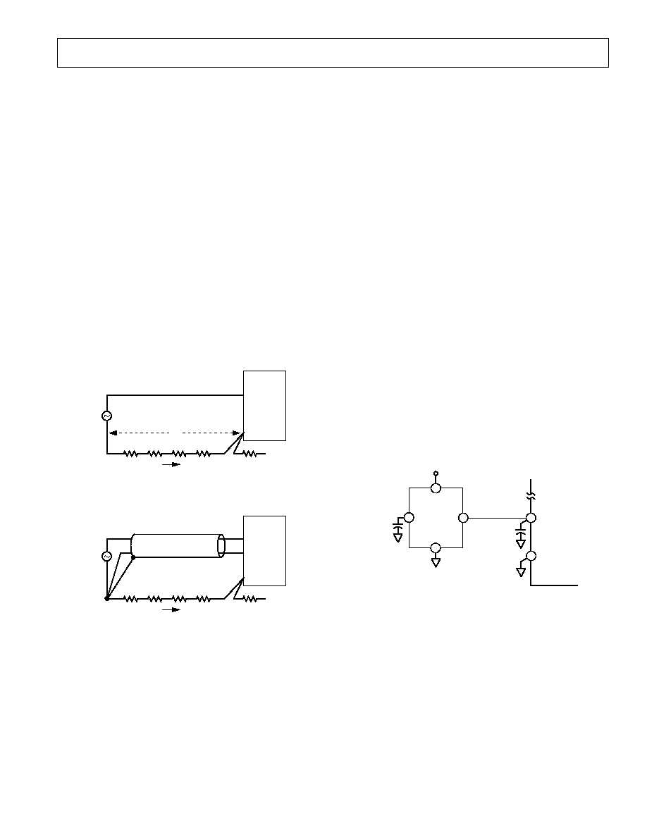
AD676. Figure 8 represents a circuit, based upon the AD845,
recommended for low noise, low distortion ac applications.
For applications optimized more for low bias and low offset than
speed or bandwidth, the AD845 of Figure 8 may be replaced by
the OP27.
499
1k
+12V
12V
AD845
0.1
µ
F
0.1
µ
F
AGND
AGND
SENSE
±
5V
INPUT
1k
AD676
15
13
14
2
3
4
7
6
V
IN
Figure 8.
AD676
REV. A
13
AC PERFORMANCE
AC parameters, which include S/(N+D), THD, etc., reflect the
AD676's effect on the spectral content of the analog input sig-
nal. Figures 12 through 16 provide information on the AD676's
ac performance under a variety of conditions.
As a general rule, averaging the results from several conversions
reduces the effects of noise, and therefore improves such param-
eters as S/(N+D). AD676 performance may be optimized by
operating the device at its maximum sample rate of 100 kSPS
and digitally filtering the resulting bit stream to the desired signal
bandwidth. This succeeds in distributing noise over a wider
frequency range, thus reducing the noise density in the fre-
quency band of interest. This subject is discussed in the follow-
ing section.
OVERSAMPLING AND NOISE FILTERING
The Nyquist rate for a converter is defined as one-half its sam-
pling rate. This is established by the Nyquist theorem, which re-
quires that a signal he sampled at a rate corresponding to at
least twice its highest frequency component of interest in order
to preserve the informational content. Oversampling is a conver-
sion technique in which the sampling frequency is more than
twice the frequency bandwidth of interest. In audio applications,
the AD676 can operate at a 2 F
S
oversampling rate, where
F
S
= 48 kHz.
In quantized systems, the informational content of the analog
input is represented in the frequency spectrum from dc to the
Nyquist rate of the converter. Within this same spectrum are
higher frequency noise and signal components. Antialias, or low
pass, filters are used at the input to the ADC to reduce these
noise and signal components so that their aliased components
do not corrupt the baseband spectrum. However, wideband
noise contributed by the AD676 will not be reduced by the
antialias filter. The AD676 quantization noise is evenly distrib-
uted from dc to the Nyquist rate, and this fact can be used to
minimize its overall affect.
The AD676 quantization noise effects can be reduced by
oversamplingsampling at a rate higher than that defined by the
Nyquist theorem. This spreads the noise energy over a band-
width wider than the frequency band of interest. By judicious
selection of a digital decimation filter, noise frequencies outside
the bandwidth of interest may be eliminated.
The process of analog to digital conversion inherently produces
noise, known as quantization noise. The magnitude of this noise
is a function of the resolution of the converter, and manifests it-
self as a limit to the theoretical signal-to-noise ratio achievable.
This limit is described by S/(N+D) = (6.02n + 1.76 + 10 log
F
S
/2F
A
) dB, where n is the resolution of the converter in bits, F
S
is the sampling frequency, and Fa is the signal bandwidth of in-
terest. For audio bandwidth applications, the AD676 is capable
of operating at a 2 oversample rate (96 kSPS), which typically
produces an improvement in S/(N+D) of 3 dB compared with
operating at the Nyquist conversion rate of 48 kSPS. Over-
sampling has another advantage as well; the demands on the
antialias filter are lessened. In summary, system performance is
optimized by running the AD676 at or near its maximum sam-
pling rate of 100 kHz and digitally filtering the resulting spec-
trum to eliminate undesired frequencies.
DC CODE UNCERTAINTY
Ideally, a fixed dc input should result in the same output code
for repetitive conversions. However, as a consequence of system
noise and circuit noise, for a given input voltage there is a range
of output codes which may occur. Figure 9 is a histogram of the
codes resulting from 1000 conversions of a typical input voltage
by the AD676 used with a 10 V reference.
2
1
0
1
DEVIATION FROM CORRECT CODE LSBs
NUMBER OF CODE HITS
800
0
200
400
600
Figure 9. Distribution of Codes from 1000 Conversions,
Relative to the Correct Code
The standard deviation of this distribution is approximately 0.5
LSBs. If less uncertainty is desired, averaging multiple conver-
sions will narrow this distribution by the inverse of the square
root of the number of samples; i.e., the average of 4 conversions
would have a standard deviation of 0.25 LSBs.
AD676
REV. A
14
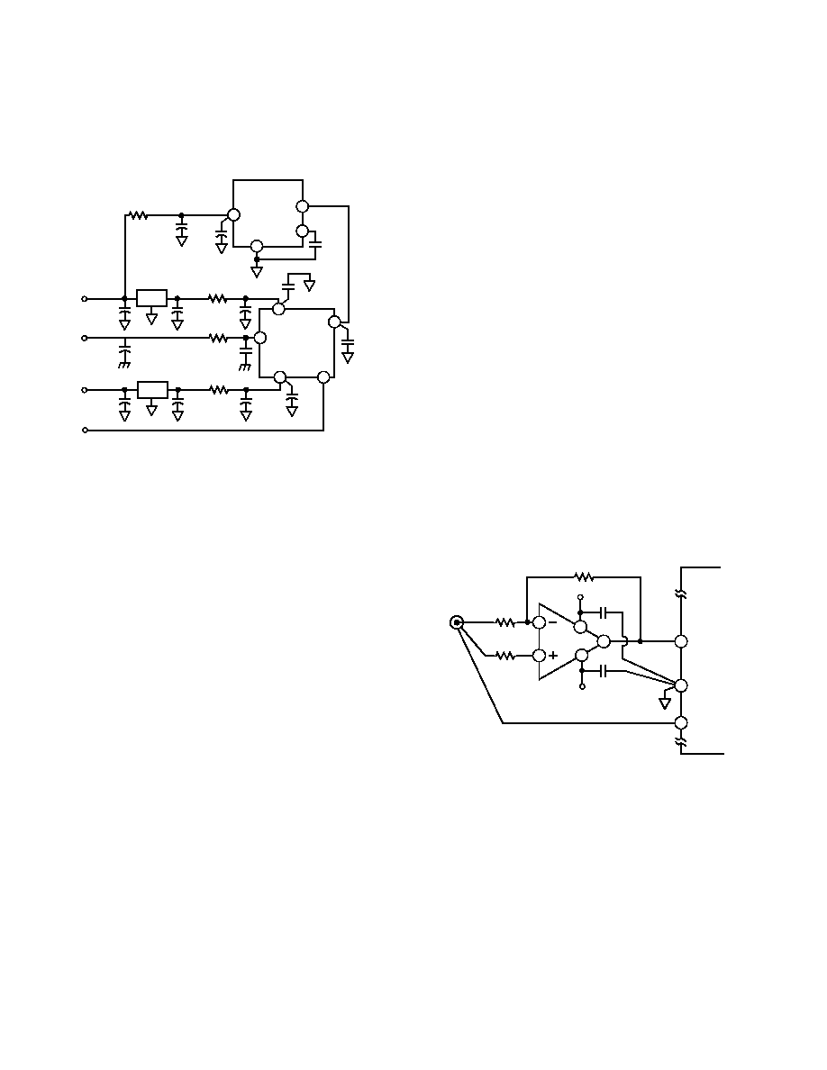
MICROPROCESSOR INTERFACE
The AD676 is ideally suited for use in both traditional dc mea-
surement applications supporting a microprocessor, and in ac
signal processing applications interfacing to a digital signal pro-
cessor. The AD676 is designed to interface with a 16-bit data
bus, providing all output data bits in a single read cycle. A vari-
ety of external buffers, such as 74HC541, can be used with the
AD676 to provide 3-state outputs, high driving capability, and
to prevent bus noise from coupling into the ADC. The following
sections illustrate the use of the AD676 with a representative
digital signal processor and microprocessor. These circuits pro-
vide general interface practices which are applicable to other
processor choices.
ADSP-2101
Figure 10a shows the AD676 interfaced to the ADSP-2101 DSP
processor. The AD676 buffers are mapped in the ADSP-2101's
memory space, requiring one wait state when using a 12.5 MHz
processor clock.
The falling edge of BUSY interrupts the processor, indicating
that new data is ready. The ADSP-2101 automatically jumps to
the appropriate service routine with minimal overhead. The in-
terrupt routine then instructs the processor to read the new data
using a memory read instruction.
A0
A13
D8 D23
ADSP-2101
IRQ2
RD
DMS
DECODER
CS
ADDRESS BUS
Y1 Y8
A1 A3
74HC541
G1
G2
Y1 Y8
A1 A3
74HC541
G1
G2
BUSY
BIT 1 BIT 16
AD676
16
8
8
8
16
8
Figure 10a.
Figure 10b shows circuitry which would be included by a typical
address decoder for the output buffers. In this case, a data
memory access to any address in the range 3000H to 37FFH
will result in the output buffers being enabled.
The AD676 CLK and SAMPLE can be generated by dividing
down the system clock as described earlier (Figure 3), or if the
ADSP-2101 serial port clocks are not being used, they can be
programmed to generate CLK and SAMPLE.
A13
A12
A11
DMS
CS
Figure 10b.
80286
The 80286 16-bit microprocessor can be interfaced to a buff-
ered AD676 without any generation of wait states. As seen in
Figure 11, BUSY can be used both to control the AD676 clock
and to alert the processor when new data is ready. In the system
shown, the 80286 should be configured in an edge triggered, di-
rect interrupt mode (integrated controller provides the interrupt
vector). Since the 80286 does not latch interrupt signals, the in-
terrupt needs to be internally acknowledged before BUSY goes
HIGH again during the next AD676 conversion (BUSY = 0).
Depending on whether the AD676 buffers are mapped into
memory or 1/0 space, the interrupt service routine will read the
data by using either the MOV or the IN instruction. To be able
to read all the 16 bits at once, and thereby increase the 80286's
efficiency, the buffers should be located at an even address.
AD0 AD15
ALE
CLKOUT
INT 0
80286
RD
PCSO 6
S2
DECODER
CS
16
Y1 Y8
A1 A8
74HC541
G1
G2
Y1 Y8
A1 A8
74HC541
G1
G2
8
8
DIVIDER
D
CLR
Q
Q
D
CLR
Q
Q
74HC04
74HC74
BIT1 BIT16
SAMPLE
CLK
BUSY
AD676
2MHz
16
8
8
Figure 11.
AD676
REV. A
15
102
80
10.5
86
82
3.5
84
2.5
92
88
90
94
96
98
100
9.5
8.5
7.5
6.5
5.5
4.5
THD
S/(N+D)
V Volts
REF
dB
Figure 12. S/(N+D) and THD vs. V
REF
Figure 14. 4096 Point FFT at 96 kSPS, f
IN
= 1.06 kHz
100
30
0
60
40
50
60
90
70
80
10
20
30
40
50
THD
S/(N+D)
INPUT AMPLITUDE dB
dB
Figure 13. S/(N+D) and THD vs. Input Amplitude
Figure 15. IMD Plot for f
IN
= 1008 Hz (fa),
1055 Hz (fb) at 96 kSPS
90
80
70
60
50
RIPPLE FREQUENCY Hz
S/(N+D) dB
0
100
1k
10k
100k
1M
30
20
40
+5V
+12V
12V
Figure 16. AC Power Supply Rejection (f
IN
= 1.06 kHz)
f
SAMPLE
= 96 kSPS, V
RIPPLE
= 0.13 V p-p
Typical Dynamic Performance
AD676
REV. A
16
OUTLINE DIMENSIONS
Dimensions shown in inches and (mm).
28-Pin Ceramic DIP Package (D-28)
0.225 (5.72)
MAX
0.150 (3.81)
MIN
0.100 (2.54)
BSC
1.490 (37.85) MAX
0.200 (5.08)
0.125 (3.18)
0.070 (1.78)
0.030 (0.76)
0.060 (1.52)
0.015 (0.38)
0.610 (15.49)
0.500 (12.70)
0.620 (15.75)
0.590 (14.99)
0.018 (0.46)
0.008 (0.20)
28
1
15
14
0.005 (0.13)
MIN
0.100 (2.54)
MAX
0.026 (0.66)
0.014 (0.36)
C1679247/92
PRINTED IN U.S.A.