 | ÐлекÑÑоннÑй компоненÑ: AD706AN | СкаÑаÑÑ:  PDF PDF  ZIP ZIP |
Äîêóìåíòàöèÿ è îïèñàíèÿ www.docs.chipfind.ru
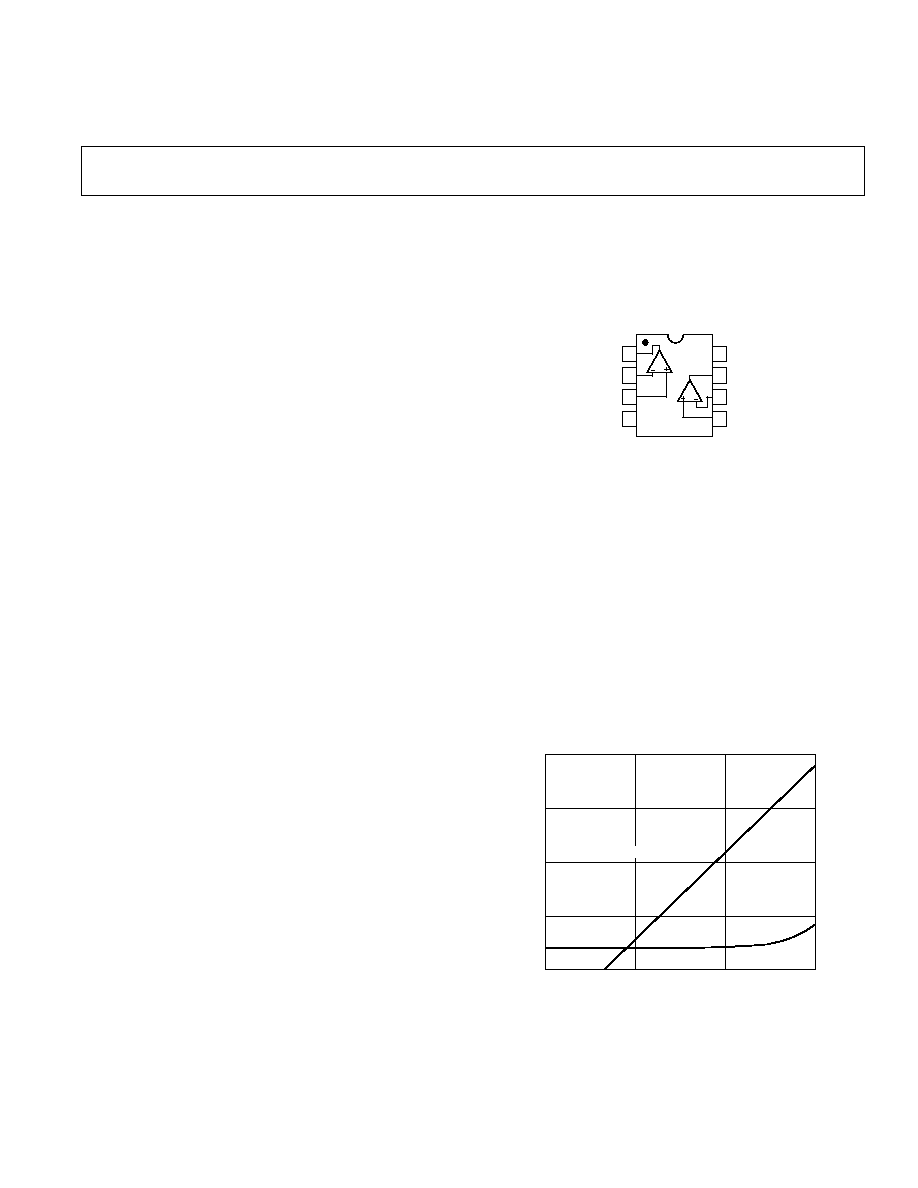
CONNECTION DIAGRAM
Plastic Mini-DIP (N)
Cerdip (Q) and
Plastic SOIC (R) Packages
TOP VIEW
OUTPUT
IN
IN
V
OUTPUT
IN
IN
V
AD706
1
2
3
4
8
7
6
5
AMPLIFIER 1
AMPLIFIER 2
a
AD706
FEATURE
HIGH DC PRECISION
50 V max Offset Voltage
0.6 V/ C max Offset Drift
110 pA max Input Bias Current
LOW NOISE
0.5 V p-p Voltage Noise, 0.1 Hz to 10 Hz
LOW POWER
750 A Supply Current
Available in 8-Lead Plastic Mini-DlP, Hermetic Cerdip
and Surface Mount (SOIC) Packages
Available in Tape and Reel in Accordance with
EIA-481A Standard
Single Version: AD705, Quad Version: AD704
PRIMARY APPLICATIONS
Low Frequency Active Filters
Precision Instrumentation
Precision Integrators
PRODUCT DESCRIPTION
The AD706 is a dual, low power, bipolar op amp that has the
low input bias current of a BiFET amplifier, but which offers a
significantly lower I
B
drift over temperature. It utilizes superbeta
bipolar input transistors to achieve picoampere input bias cur-
rent levels (similar to FET input amplifiers at room tempera-
ture), while its I
B
typically only increases by 5
×
at 125
°
C (unlike
a BiFET amp, for which I
B
doubles every 10
°
C for a 1000
×
increase at 125
°
C). The AD706 also achieves the microvolt
offset voltage and low noise characteristics of a precision bipolar
input amplifier.
Since it has only 1/20 the input bias current of an OP07, the
AD706 does not require the commonly used "balancing" resis-
tor. Furthermore, the current noise is 1/5 that of the OP07,
which makes this amplifier usable with much higher source
impedances. At 1/6 the supply current (per amplifier) of the
OP07, the AD706 is better suited for today's higher density
boards.
The AD706 is an excellent choice for use in low frequency
active filters in 12- and 14-bit data acquisition systems, in preci-
sion instrumentation and as a high quality integrator. The
AD706 is internally compensated for unity gain and is available
in five performance grades. The AD706J and AD706K are rated
over the commercial temperature range of 0
°
C to +70
°
C. The
AD706A and AD706B are rated over the industrial temperature
range of 40
°
C to +85
°
C.
The AD706 is offered in three varieties of an 8-lead package:
plastic mini-DIP, hermetic cerdip and surface mount (SOIC).
"J" grade chips are also available.
PRODUCT HIGHLIGHTS
1. The AD706 is a dual low drift op amp that offers BiFET
level input bias currents, yet has the low I
B
drift of a bipolar
amplifier. It may be used in circuits using dual op amps such
as the LT1024.
2. The AD706 provides both low drift and high dc precision.
3. The AD706 can be used in applications where a chopper
amplifier would normally be required but without the
chopper's inherent noise.
Dual Picoampere Input
Current Bipolar Op Amp
One Technology Way, P.O. Box 9106, Norwood, MA 02062-9106, U.S.A.
Tel: 781/329-4700
World Wide Web Site: http://www.analog.com
Fax: 781/326-8703
© Analog Devices, Inc., 1997
REV. C
Information furnished by Analog Devices is believed to be accurate and
reliable. However, no responsibility is assumed by Analog Devices for its
use, nor for any infringements of patents or other rights of third parties
which may result from its use. No license is granted by implication or
otherwise under any patent or patent rights of Analog Devices.
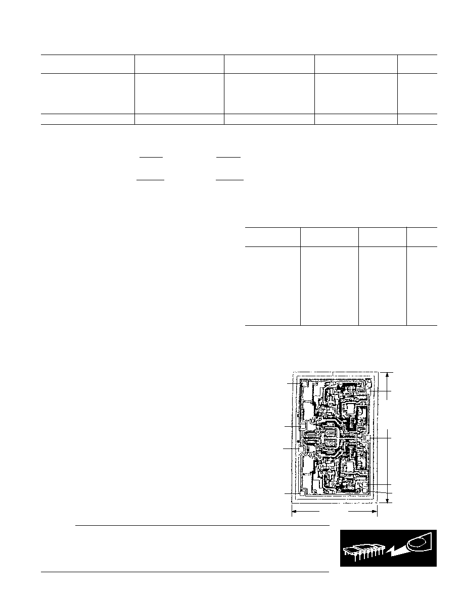
TEMPERATURE C
100
0.01
TYPICAL I
B
nA
1
0.1
10
55
+125
+25
+110
TYPICAL JFET AMP
AD706
Figure 1. Input Bias Current vs. Temperature
AD706SPECIFICATIONS
AD706J/A
AD706K/B
Parameter
Conditions
Min
Typ
Max
Min
Typ
Max
Units
INPUT OFFSET VOLTAGE
Initial Offset
30
100
10
50
µ
V
Offset
T
MIN
to T
MAX
40
150
25
100
µ
V
vs. Temp, Average TC
0.2
1.5
0.2
0.6
µ
V/
°
C
vs. Supply (PSRR)
V
S
=
±
2 V to
±
18 V
110
132
112
132
dB
T
MIN
to T
MAX
V
S
=
±
2.5 V to
±
18 V
106
126
108
126
dB
Long Term Stability
0.3
0.3
µ
V/Month
INPUT BIAS CURRENT
1
V
CM
= 0 V
50
200
30
110
pA
V
CM
=
±
13.5 V
250
160
pA
vs. Temp, Average TC
0.3
0.2
pA/
°
C
T
MIN
to T
MAX
V
CM
= 0 V
300
200
pA
T
MIN
to T
MAX
V
CM
=
±
13.5 V
400
300
pA
INPUT OFFSET CURRENT
V
CM
= 0 V
30
150
30
100
pA
V
CM
=
±
13.5 V
250
200
pA
vs. Temp, Average TC
0.6
0.4
pA/
°
C
T
MIN
to T
MAX
V
CM
= 0 V
80
250
80
200
pA
T
MIN
to T
MAX
V
CM
=
±
13.5 V
80
350
80
300
pA
MATCHING CHARACTERISTICS
Offset Voltage
150
75
µ
V
T
MIN
to T
MAX
250
150
µ
V
Input Bias Current
2
300
150
pA
T
MIN
to T
MAX
500
250
pA
Common-Mode Rejection
106
110
dB
T
MIN
to T
MAX
106
108
dB
Power Supply Rejection
106
110
dB
T
MIN
to T
MAX
104
106
dB
Crosstalk
@ f = 10 Hz
(Figure 19a)
R
L
= 2 k
150
150
dB
FREQUENCY RESPONSE
Unity Gain Crossover
Frequency
0.8
0.8
MHz
Slew Rate
G = 1
0.15
0.15
V/
µ
s
T
MIN
to T
MAX
0.15
0.15
V/
µ
s
INPUT IMPEDANCE
Differential
40 2
40 2
M
pF
Common Mode
300 2
300 2
G
pF
INPUT VOLTAGE RANGE
Common-Mode Voltage
±
13.5
±
14
±
13.5
±
14
V
Common-Mode Rejection
Ratio
V
CM
=
±
13.5 V
110
132
114
132
dB
T
MIN
to T
MAX
108
128
108
128
dB
INPUT CURRENT NOISE
0.1 Hz to 10 Hz
3
3
pA p-p
f = 10 Hz
50
50
fA/
Hz
INPUT VOLTAGE NOISE
0.1 Hz to 10 Hz
0.5
0.5
1.0
µ
V p-p
f = 10 Hz
17
17
nV/
Hz
f = 1 kHz
15
22
15
22
nV/
Hz
OPEN-LOOP GAIN
V
O
=
±
12 V
R
LOAD
= 10 k
200
2000
400
2000
V/mV
T
MIN
to T
MAX
150
1500
300
1500
V/mV
V
O
=
±
10 V
R
LOAD
=
2 k
200
1000
300
1000
V/mV
T
MIN
to T
MAX
150
1000
200
1000
V/mV
OUTPUT CHARACTERISTICS
Voltage Swing
R
LOAD
= 10 k
±
13
±
14
±
13
±
14
V
T
MIN
to T
MAX
±
13
±
14
±
13
±
14
V
Current
Short Circuit
±
15
±
15
mA
Capacitive Load
Drive Capability
Gain = +1
10,000
10,000
pF
(@ T
A
= +25 C, V
CM
= 0 V and 15 V dc, unless otherwise noted)
REV. C
2
AD706J/A
AD706K/B
Parameter
Conditions
Min
Typ
Max
Min
Typ
Max
Units
POWER SUPPLY
Rated Performance
±
15
±
15
V
Operating Range
±
2.0
±
18
±
2.0
±
18
V
Quiescent Current, Total
0.75
1.2
0.75
1.2
mA
T
MIN
to T
MAX
0.8
1.4
0.8
1.4
mA
TRANSISTOR COUNT
# of Transistors
90
90
NOTES
l
Bias current specifications are guaranteed maximum at either input.
2
Input bias current match is the difference between corresponding inputs (I
B
of IN of Amplifier #1 minus I
B
of IN of Amplifier #2).
CMRR match is the difference between
V
OS
#1
V
CM
for amplifier #1 and
V
OS
# 2
V
CM
for amplifier #2 expressed in dB.
PSRR match is the difference between
V
OS
#1
V
SUPPLY
for amplifier #l and
V
OS
# 2
V
SUPPLY
for amplifier #2 expressed in dB.
All min and max specifications are guaranteed.
Specifications subject to change without notice.
AD706
ABSOLUTE MAXIMUM RATINGS
l
Supply Voltage . . . . . . . . . . . . . . . . . . . . . . . . . . . . . . . .
±
18 V
Internal Power Dissipation
(Total: Both Amplifiers)
2
. . . . . . . . . . . . . . . . . . . . 650 mW
Input Voltage . . . . . . . . . . . . . . . . . . . . . . . . . . . . . . . . . .
±
V
S
Differential Input Voltage
3
. . . . . . . . . . . . . . . . . . . . +0.7 Volts
Output Short Circuit Duration . . . . . . . . . . . . . . . . Indefinite
Storage Temperature Range (Q) . . . . . . . . . 65
°
C to +150
°
C
Storage Temperature Range (N, R) . . . . . . . 65
°
C to +125
°
C
Operating Temperature Range
AD706J/K . . . . . . . . . . . . . . . . . . . . . . . . . . . 0
°
C to +70
°
C
AD706A/B . . . . . . . . . . . . . . . . . . . . . . . . . 40
°
C to +85
°
C
Lead Temperature (Soldering 10 secs) . . . . . . . . . . . . +300
°
C
NOTES
1
Stresses above those listed under Absolute Maximum Ratings may cause perma-
nent damage to the device. This is a stress rating only; functional operation of the
device at these or any other conditions above those indicated in the operational
section of this specification is not implied. Exposure to absolute maximum rating
conditions for extended periods may affect device reliability.
2
Specification is for device in free air:
8-Lead Plastic Package:
JA
= 100
°
C/Watt
8-Lead Cerdip Package:
JA
= 110
°
C/Watt
8-Lead Small Outline Package:
JA
= 155
°
C/Watt
3
The input pins of this amplifier are protected by back-to-back diodes. If the
differential voltage exceeds
±
0.7 volts, external series protection resistors should
be added to limit the input current to less than 25 mA.
ORDERING GUIDE
Temperature
Package
Model
Range
Description
Option*
AD706AN
40
°
C to +85
°
C
Plastic DIP
N-8
AD706JN
0
°
C to +70
°
C
Plastic DIP
N-8
AD706KN
0
°
C to +70
°
C
Plastic DIP
N-8
AD706JR
0
°
C to +70
°
C
SOIC
R-8
AD706JR-REEL
0
°
C to +70
°
C
Tape and Reel
AD706AQ
40
°
C to +85
°
C
Cerdip
Q-8
AD706BQ
40
°
C to +85
°
C
Cerdip
Q-8
AD706AR
40
°
C to +85
°
C
SOIC
R-8
AD706AR-REEL 40
°
C to +85
°
C
Tape and Reel
*N = Plastic DIP; Q = Cerdip, R = Small Outline Package.
CAUTION
ESD (electrostatic discharge) sensitive device. Electrostatic charges as high as 4000 V readily
accumulate on the human body and test equipment and can discharge without detection.
Although the AD706 features proprietary ESD protection circuitry, permanent damage may
occur on devices subjected to high energy electrostatic discharges. Therefore, proper ESD
precautions are recommended to avoid performance degradation or loss of functionality.
METALIZATION PHOTOGRAPH
Dimensions shown in inches and (mm).
Contact factory for latest dimensions.
REV. C
3
2
1
3
4
5
6
7
8
OUTPUT A
INPUT A
+INPUT A
V
S
0.074 (1.88)
OUTPUT B
INPUT B
+INPUT B
0.118 (3.00)
+V
S
WARNING!
ESD SENSITIVE DEVICE
AD706Typical Characteristics
(@ +25 C, V
S
= 15 V, unless otherwise noted)
REV. C
4
SAMPLE
SIZE: 3000
INPUT OFFSET VOLTAGE V
NUMBER OF UNITS
1000
0
80
40
0
40
80
400
200
600
800
Figure 2. Typical Distribution of Input
Offset Voltage
SUPPLY VOLTAGE Volts
V
S
0
5
10
15
20
1.5
1.0
0.5
1.0
0.5
1.5
INPUT COMMON-MODE VOLTAGE LIMIT Volts
(REFERRED TO SUPPLY VOLTAGES)
V
S
Figure 5. Input Common-Mode
Voltage Range vs. Supply Voltage
OFFSET VOLTAGE DRIFT V/ C
200
0
0.8
0.4
0
0.4
0.8
80
40
120
160
SAMPLE SIZE: 375
55 C TO 125 C
NUMBER OF UNITS
Figure 8. Typical Distribution of
Offset Voltage Drift
INPUT BIAS CURRENT pA
NUMBER OF UNITS
1000
0
160
80
0
80
160
400
200
600
800
SAMPLE
SIZE: 5100
Figure 3. Typical Distribution of
Input Bias Current
FREQUENCY Hz
OUTPUT VOLTAGE Volts p-p
35
30
0
1k
10k
1M
100k
25
20
15
10
5
Figure 6. Large Signal Frequency
Response
WARM-UP TIME Minutes
4
0
0
1
2
3
4
2
3
1
CHANGE IN OFFSET VOLTAGE
V
5
Figure 9. Change in Input Offset
Voltage vs. Warm-Up Time
INPUT OFFSET CURRENT pA
NUMBER OF UNITS
1000
0
120
60
0
60
120
400
200
600
800
SAMPLE SIZE: 2400
Figure 4. Typical Distribution of
Input Offset Current
SOURCE RESISTANCE
OFFSET VOLTAGE DRIFT
V/
C
100
10
0.1
1k
10k
100M
1.0
100k
1M
10M
SOURCE RESISTANCE
MAY BE EITHER BALANCED
OR UNBALANCED
FOR INDUSTRIAL
TEMPERATURE
RANGE
Figure 7. Offset Voltage Drift vs.
Source Resistance
COMMON-MODE VOLTAGE Volts
60
60
15
10
5
0
5
20
40
0
INPUT BIAS CURRENT pA
10
20
40
15
NEGATIVE I
B
POSITIVE I
B
Figure 10. Input Bias Current vs.
Common-Mode Voltage
AD706
REV. C
5
FREQUENCY Hz
1000
100
1
1
10
1000
100
10
VOLTAGE NOISE nV/
Hz
Figure 11. Input Noise Voltage
Spectral Density
SUPPLY VOLTAGE Volts
1000
600
0
5
10
15
20
800
900
700
QUIESCENT CURRENT
A
+125 C
55 C
+25 C
Figure 14. Quiescent Supply Current
vs. Supply Voltage
LOAD RESISTANCE k
OPEN-LOOP VOLTAGE GAIN
10M
1M
100k
1
2
4
6 8 10
100
+125 C
+25 C
55 C
Figure 17. Open-Loop Gain vs. Load
Resistance vs. Load Resistance
FREQUENCY Hz
1000
100
1
1
10
1000
100
10
CURRENT NOISE fA/
Hz
100
10k
20M
V
OUT
Figure 12. Input Noise Current
Spectral Density
FREQUENCY Hz
+160
0
0.1
1
10
100
10k
+120
+140
+100
100k
+80
CMRR dB
+60
1M
+40
+20
1k
Figure 15. Common-Mode Rejection
Ratio vs. Frequency
FREQUENCY Hz
140
20
0.01 0.1
1
10
1k
100
120
80
10k
60
40
1M
20
0
100
OPEN-LOOP VOLTAGE GAIN dB
100k
10M
GAIN
PHASE
0
30
60
90
120
150
180
PHASE SHIFT De
g
rees
210
240
Figure 18. Open-Loop Gain and
Phase Shift vs. Frequency
TIME Seconds
0
5
10
0.5 V
Figure 13. 0.1 Hz to 10 Hz Noise
Voltage
FREQUENCY Hz
180
20
0.1
1
10
100
10k
140
160
120
100k
100
80
1M
60
40
1k
PSRR dB
+ PSRR
PSRR
Figure 16. Power Supply Rejection
Ratio vs. Frequency
SUPPLY VOLTAGE
Volts
+V
S
0
5
10
15
20
1.5
1.0
0.5
+1.0
+0.5
+1.5
OUTPUT VOLTAGE SWING Volts
(REFERRED TO SUPPLY VOLTAGES)
V
S
Figure 19. Output Voltage Swing vs.
Supply Voltage
AD706
REV. C
6
FREQUENCY Hz
80
160
10
100
1k
10k
100k
120
100
140
CROSSTALK dB
Figure 20a. Crosstalk vs. Frequency
3
2
4
1
SINE WAVE
GENERATOR
1/2
AD706
0.1 F
+V
S
0.1 F
R
L
2k
V
S
20V p-p
V
OUT
#1
20k
6
5
7
8
1 F
0.1 F
+V
S
2.21k
CROSSTALK = 20 LOG
10
20dB
V
OUT
#2
V
OUT
#2
V
OUT
#1
1/2
AD706
Figure 20b. Crosstalk Test Circuit
FREQUENCY Hz
1000
0.1
1
10
100
1k
10k
10
100
1
CLOSED-LOOP OUTPUT IMPEDANCE
0.001
0.01
100k
AV = 1000
AV = + 1
I
OUT
= +1mA
Figure 21. Magnitude of Closed-Loop Output Impedance
vs. Frequency
4
0.1 F
+V
S
8
1/2
AD706
V
IN
0.1 F
R
L
2k
C
L
V
OUT
R
F
SQUARE
WAVE
INPUT
V
S
Figure 22a. Unity Gain Follower (For Large Signal
Applications, Resistor R
F
Limits the Current
Through the Input Protection Diodes)
Figure 22b. Unity Gain Follower
Large Signal Pulse Response, R
F
=
10 k
, C
L
= 1,000 pF
Figure 22c. Unity Gain Follower
Small Signal Pulse Response, R
F
=
0
, C
L
= 100 pF
Figure 22d. Unity Gain Follower
Small Signal Pulse Response, R
F
=
0
, C
L
= 1000 pF
AD706
REV. C
7
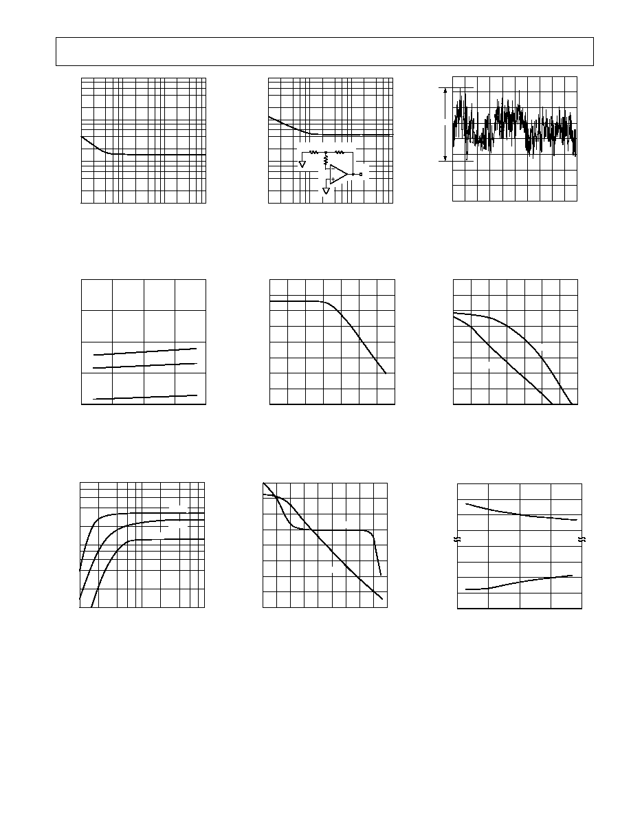
Figure 24 shows an in-amp circuit that has the obvious advan-
tage of requiring only one AD706, rather than three op amps,
with subsequent savings in cost and power consumption. The
transfer function of this circuit (without R
G
) is:
V
OUT
=
(V
IN #1
-
V
IN #2
) 1
+
R4
R3
for R1 = R4 and R2 = R3
Input resistance is high, thus permitting the signal source to
have an unbalanced output impedance.
+V
S
0.1 F
1k
+
A1
AD706
1/2
R
P
*
1k
49.9k
R2
R3
R4
V
IN#1
R
G
(OPTIONAL)
R1
49.9k
A2
+
0.1 F
AD706
1/2
OUTPUT
*OPTIONAL INPUT PROTECTION RESISTOR FOR GAINS GREATER
THAN 100 OR INPUT VOLTAGES EXCEEDING THE SUPPLY VOLTAGE.
V
OUT
= (V
IN#1
V
IN#2
) (1+ ) + ( )
FOR R1 = R4, R2 = R3
R4
R3
2R4
R
G
V
S
R
P
*
V
IN#2
3
2
8
1
5
6
7
4
Figure 24. A Two Op-Amp Instrumentation Amplifier
Furthermore, the circuit gain may be fine trimmed using an
optional trim resistor, R
G
. Like the three op-amp circuit, CMR
Figure 23a. Unity Gain Inverter Connection
Figure 23b. Unity Gain Inverter Large
Signal Pulse Response, C
L
= 1,000 pF
Figure 23c. Unity Gain Inverter Small
Signal Pulse Response, C
L
= 100 pF
Figure 23d. Unity Gain Inverter Small
Signal Pulse Response, C
L
= 1000 pF
increases with gain, once initial trimming is accomplished--but
CMR is still dependent upon the ratio matching of Resistors R1
through R4. Resistor values for this circuit, using the optional
gain resistor, R
G
, can be calculated using:
R1
=
R4
=
49.9 k
R2
=
R3
=
49.9 k
0.9 G
-
1
R
G
=
99.8 k
0.06 G
where G = Desired Circuit Gain
Table I provides practical 1% resistance values. (Note that
without resistor R
G
, R2 and R3 = 49.9 k
/G1.)
Table I. Operating Gains of Amplifiers A1 and A2 and
Practical 1% Resistor Values for the Circuit of Figure 24
Circuit Gain
Gain of A1
Gain of A2
R2, R3
R1, R4
1.10
11.00
1.10
499 k
49.9 k
1.33
4.01
1.33
150 k
49.9 k
1.50
3.00
1.50
100 k
49.9 k
2.00
2.00
2.00
49.9 k
49.9 k
10.1
1.11
10.10
5.49 k
49.9 k
101.0
1.01
101.0
499
49.9 k
1001
1.001
1001
49.9
49.9 k
For a much more comprehensive discussion of in-amp applica-
tions, refer to the Instrumentation Amplifier Applications Guide--
available free from Analog Devices, Inc.
10k
+
AD706
+
0.1µF
8
4
V
IN
V
OUT
+V
S
10k
C
L
1/2
0.1 F
R
L
2.5k
SQUARE
WAVE
INPUT
V
S
AD706
REV. C
8
C1429b212/97
PRINTED IN U.S.A.
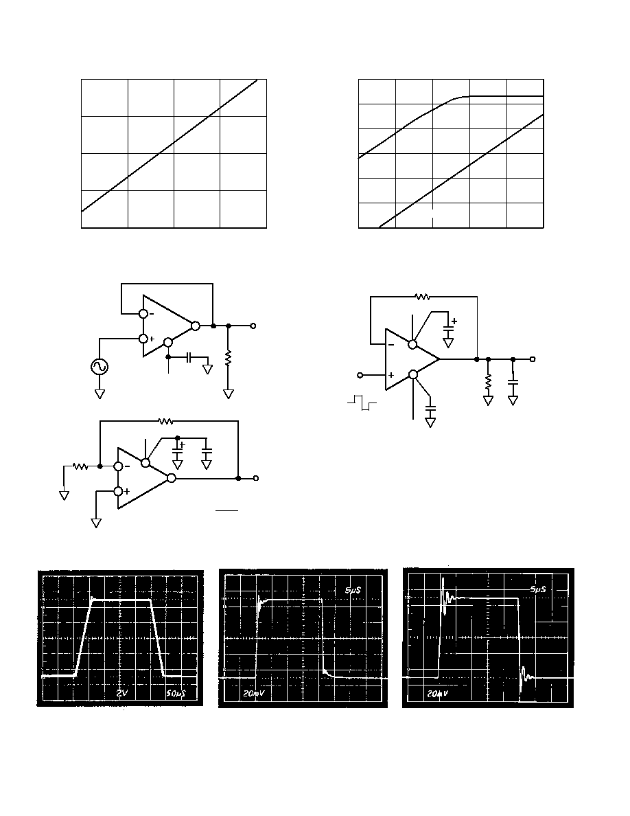
A 1 Hz, 4-Pole, Active Filter
Figure 25 shows the AD706 in an active filter application. An
important characteristic of the AD706 is that both the input bias
current, input offset current and their drift remain low over
most of the op amp's rated temperature range. Therefore, for
most applications, there is no need to use the normal balancing
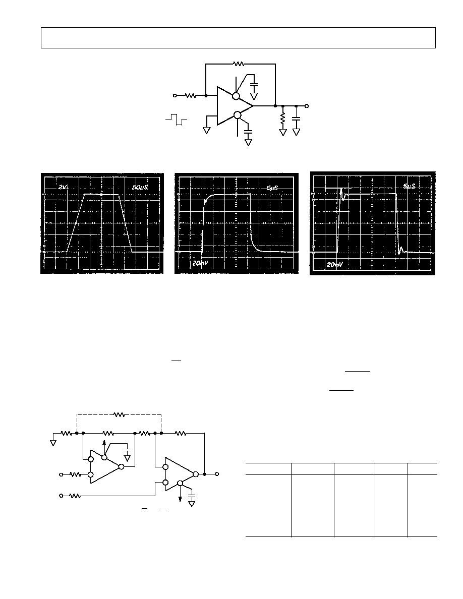
resistor. Adding the balancing resistor enhances performance at
high temperatures, as shown by Figure 26.
Table II. 1 Hz, 4-Pole, Low Pass Filter Recommended Component Values
Section 1
Section 2
Desired Low
Frequency
Frequency
C1
C2
C3
C4
Pass Response
(Hz)
Q
(Hz)
Q
( F)
( F)
( F)
( F)
Bessel
1.43
0.522
1.60
0.806
0.116
0.107
0.160
0.0616
Butterworth
1.00
0.541
1.00
1.31
0.172
0.147
0.416
0.0609
0.1 dB Chebychev
0.648
0.619
0.948
2.18
0.304
0.198
0.733
0.0385
0.2 dB Chebychev
0.603
0.646
0.941
2.44
0.341
0.204
0.823
0.0347
0.5 dB Chebychev
0.540
0.705
0.932
2.94
0.416
0.209
1.00
0.0290
1.0 dB Chebychev
0.492
0.785
0.925
3.56
0.508
0.206
1.23
0.0242
NOTE
Specified Values are for a 3 dB point of 1.0 Hz. For other frequencies simply scale capacitors C1 through C4 directly, i.e.: for 3 Hz
Bessel response, C1 = 0.0387
µ
F, C2 = 0.0357
µ
F, C3 = 0.0533
µ
F, C4 = 0.0205
µ
F.
OUTLINE DIMENSIONS
Dimensions shown in inches and (mm).
Cerdip
(Q-8)
OUTPUT
*WITHOUT THE NETWORK,
PINS 1 & 2, AND 6 & 7 OF THE
AD706 ARE TIED TOGETHER.
CAPACITORS C1 & C2
ARE SOUTHERN ELECTRONICS
MPCC, POLYCARB 5%, 50 VOLT
+
C4
C3
0.1 F
+V
S
OPTIONAL BALANCE
RESISTOR NETWORKS*
1/2
AD706
1/2
AD706
INPUT
C1
C2
+
R1
1M
0.1 F
R2
1M
R3
1M
R4
1M
V
S
R5
2M
C5
0.01 F
3
2
4
1
5
6
7
8
R6
2M
C6
0.01 F
Figure 25. A 1 Hz, 4-Pole Active Filter
TEMPERATURE C
180
40
0
+40
60
120
0
60
120
180
OFFSET VOLTAGE OF FILTER CIRCUIT (RTI)
V
+80
+120
WITHOUT OPTIONAL
BALANCE RESISTOR, R3
WITH OPTIONAL BALANCE
RESISTOR, R3
Figure 26. V
OS
vs. Temperature Performance
of the 1 Hz Filter
Plastic Mini-DIP
(N-8)
SOIC
(R-8)
8
1
4
5
0.310 (7.87)
0.220 (5.59)
PIN 1
0.005 (0.13)
MIN
0.055 (1.4)
MAX
SEATING
PLANE
0.023 (0.58)
0.014 (0.36)
0.200 (5.08)
MAX
0.150
(3.81)
MIN
0.070 (1.78)
0.030 (0.76)
0.200 (5.08)
0.125 (3.18)
0.100
(2.54)
BSC
0.060 (1.52)
0.015 (0.38)
0.405 (10.29)
MAX
15
°
0
°
0.320 (8.13)
0.290 (7.37)
0.015 (0.38)
0.008 (0.20)
8
1
4
5
0.430 (10.92)
0.348 (8.84)
0.280 (7.11)
0.240 (6.10)
PIN 1
SEATING
PLANE
0.022 (0.558)
0.014 (0.356)
0.060 (1.52)
0.015 (0.38)
0.210 (5.33)
MAX
0.130
(3.30)
MIN
0.070 (1.77)
0.045 (1.15)
0.100
(2.54)
BSC
0.160 (4.06)
0.115 (2.93)
0.325 (8.25)
0.300 (7.62)
0.015 (0.381)
0.008 (0.204)
0.195 (4.95)
0.115 (2.93)
8
5
4
1
0.1968 (5.00)
0.1890 (4.80)
0.1574 (4.00)
0.1497 (3.80)
0.2440 (6.20)
0.2284 (5.80)
PIN 1
SEATING
PLANE
0.0098 (0.25)
0.0040 (0.10)
0.0192 (0.49)
0.0138 (0.35)
0.102 (2.59)
0.094 (2.39)
0.0500
(1.27)
BSC
0.0098 (0.25)
0.0075 (0.19)
0.0500 (1.27)
0.0160 (0.41)
8
°
0
°
0.0196 (0.50)
0.0099 (0.25)
x 45
°