 | –≠–ª–µ–∫—Ç—Ä–æ–Ω–Ω—ã–π –∫–æ–º–ø–æ–Ω–µ–Ω—Ç: AD707C | –°–∫–∞—á–∞—Ç—å:  PDF PDF  ZIP ZIP |

CONNECTION DIAGRAMS
TO-99 (H) Package
AD707
7
6
2
8
1
3
4
5
NULL
NULL
≠IN
+IN
≠V
S
+V
S
OUTPUT
NC
NC = NO CONNECT
NOTE: PIN 4 CONNECTED
TO CASE
Plastic (N) and
Cerdip (Q) Packages SOIC (R) Package
REV. B
Information furnished by Analog Devices is believed to be accurate and
reliable. However, no responsibility is assumed by Analog Devices for its
use, nor for any infringements of patents or other rights of third parties
which may result from its use. No license is granted by implication or
otherwise under any patent or patent rights of Analog Devices.
a
Ultralow Drift Op Amp
AD707
© Analog Devices, Inc., 1995
One Technology Way, P.O. Box 9106, Norwood, MA 02062-9106, U.S.A.
Tel: 617/329-4700
Fax: 617/326-8703
FEATURES
Very High DC Precision
15 V max Offset Voltage
0.1 V/ C max Offset Voltage Drift
0.35 V p-p max Voltage Noise (0.1 Hz to 10 Hz}
8 V/ V min Open-Loop Gain
130 dB min CMRR
120 dB min PSRR
1 nA max Input Bias Current
AC Performance
0.3 V/ s Slew Rate
0.9 MHz Closed-Loop Bandwidth
Dual Version: AD708
Available in Tape and Reel in Accordance with
EIA-481A Standard
APPLICATION HIGHLIGHTS
1. The AD707's 13 V/
µ
V typical open-loop gain and 140 dB
typical common-mode rejection ratio make it ideal for
precision instrumentation applications.
2. The precision of the AD707 makes tighter error budgets
possible at a lower cost.
3. The low offset voltage drift and low noise of the AD707 allow
the designer to amplify very small signals without sacrificing
overall system performance.
4. The AD707 can be used where chopper amplifiers are
required, but without the inherent noise and application
problems.
5. The AD707 is an improved pin-for-pin replacement for the
LT1001.
PRODUCT DESCRIPTION
The AD707 is a low cost, high precision op amp with state-of-
the-art performance that makes it ideal for a wide range of
precision applications. The offset voltage spec of less than 15
µ
V
is the best available in a bipolar op amp, and maximum input
offset current is 1.0 nA. The top grade is the first bipolar
monolithic op amp to offer a maximum offset voltage drift of
0.1
µ
V/
∞
C, and offset current drift and input bias current drift
are both specified at 25 pA/
∞
C maximum.
The AD707's open-loop gain is 8 V/
µ
V minimum over the full
±
10 V output range when driving a 1 k
load. Maximum input
voltage noise is 350 nV p-p (0.1 Hz to 10 Hz). CMRR and
PSRR are 130 dB and 120 dB minimum, respectively.
The AD707 is available in versions specified over commercial,
industrial and military temperature ranges. It is offered in 8-pin
plastic mini-DIP, small outline (SOIC), hermetic cerdip and
hermetic TO-99 metal can packages. Chips, MIL-STD-883B,
Rev. C, and tape & reel parts are also available.
1
2
3
4
8
7
6
5
AD707
NC = NO CONNECT
NULL
NC
OUTPUT
+V
S
NULL
≠IN
+IN
≠V
S
AD707
1
4
8
5
NC = NO CONNECT
NULL
NC
OUTPUT
+V
S
NULL
≠IN
+IN
≠V
S

AD707≠SPECIFICATIONS
REV. B
≠2≠
(@ +25 C and 15 V, unless otherwise noted)
AD707J/A
AD707K/B
Conditions
Min
Typ
Max
Min
Typ
Max
Units
INPUT OFFSET VOLTAGE
Initial
30
90
10
25
µ
V
vs. Temperature
0.3
1.0
0.1
0.3
µ
V/
∞
C
T
MIN
to T
MAX
50
100
15
45
µ
V
Long-Term Stability
0.3
0.3
µ
V/month
Adjustment Range
R2 = 20 k
(Figure 19)
±
4
±
4
mV
INPUT BIAS CURRENT
1.0
2.5
0.5
2.0
nA
T
MIN
to T
MAX
2.0
4.0
1.5
4.0
nA
Average Drift
15
40
15
40/40/40
pA/
∞
C
OFFSET CURRENT
V
CM
= 0 V
0.5
2.0
0.3
1.5
nA
T
MIN
to T
MAX
2.0
4.0
1.0
2.0
nA
Average Drift
2
40
1
25/25/35
pA/
∞
C
INPUT VOLTAGE NOISE
0.1 Hz to 10 Hz
0.23
0.6
0.23
0.6
µ
V p-p
f = 10 Hz
10.3
28
10.3
18
nV/
Hz
f = 100 Hz
10.0
13.0
10.0
12
nV/
Hz
f = 1 kHz
9.6
11.0
9.6
11.0
nV/
Hz
INPUT CURRENT NOISE
0.1 Hz to 10 Hz
14
35
14
30
pA p-p
f = 10 Hz
0.32
0.9
0.32
0.8
pA/
Hz
f = 100 Hz
0.14
0.27
0.14
0.23
pA/
Hz
f = 1 kHz
0.12
0.18
0.12
0.17
pA/
Hz
COMMON-MODE
REJECTION RATIO
V
CM
=
±
13 V
120
140
130
140
dB
T
MIN
to T
MAX
120
140
120
140
dB
OPEN-LOOP GAIN
V
O
=
±
10 V
R
LOAD
2 k
3
13
5
13
V/
µ
V
T
MIN
to T
MAX
3
13
3
13
V/
µ
V
POWER SUPPLY
REJECTION RATIO
V
S
=
±
3 V to
±
18 V
110
130
115
130
dB
T
MIN
to T
MAX
110
130
110
130
dB
FREQUENCY RESPONSE
Closed-Loop Bandwidth
0.4
0.9
0.4
0.9
MHz
Slew Rate
0.12
0.3
0.12
0.3
V/
µ
s
INPUT RESISTANCE
Differential
24
100
45
200
M
Common Mode
200
300
G
OUTPUT CHARACTERISTICS
Voltage
R
LOAD
10 k
13.5
14
13.5
14
±
V
R
LOAD
2 k
12.5
13.0
12.5
13.0
±
V
R
LOAD
1 k
12.0
12.5
12.0
12.5
±
V
R
LOAD
2 k
T
MIN
to T
MAX
12.0
13.0
12.0
13.0
±
V
OPEN-LOOP OUTPUT
RESISTANCE
60
60
POWER SUPPLY
Current, Quiescent
2.5
3
2.5
3
mA
Power Consumption, No Load
V
S
=
±
15 V
75
90
75
90
mW
V
S
=
±
3 V
7.5
9.0
7.5
9.0
mW
NOTES
All min and max specifications are guaranteed. Specifications in boldface are tested on all production units at final electrical test. Results from those tests are used to
calculate outgoing quality levels.
Specifications subject to change without notice.

AD707
REV. B
≠3≠
ABSOLUTE MAXIMUM RATINGS
1
Supply Voltage . . . . . . . . . . . . . . . . . . . . . . . . . . . . . . .
±
22 V
Internal Power Dissipation
2
. . . . . . . . . . . . . . . . . . . . 500 mW
Input Voltage . . . . . . . . . . . . . . . . . . . . . . . . . . . . . . . . . .
±
V
S
Output Short Circuit Duration . . . . . . . . . . . . . . . . Indefinite
Differential Input Voltage . . . . . . . . . . . . . . . . . +V
S
and ≠V
S
Storage Temperature Range (Q, H) . . . . . . ≠65
∞
C to +150
∞
C
Storage Temperature Range (N, R) . . . . . . . ≠65
∞
C to +125
∞
C
Lead Temperature Range (Soldering 60 sec) . . . . . . . +300
∞
C
NOTES
1
Stresses above those listed under "Absolute Maximum Ratings" may cause
permanent damage to the device. Exposure to absolute maximum rating condi-
tions for extended periods may affect device reliability.
2
8-pin plastic package:
JA
= 165
∞
C/Watt; 8-pin cerdip package:
JA
= 110
∞
C/Watt;
8-pin small outline package:
JA
= 155
∞
C/Watt; 8-pin header package:
JA
=
200
∞
C/Watt.
ORDERING GUIDE
Temperature
Package
Package
Model
Range
Description
Option
AD707AH
≠40
∞
C to +85
∞
C
8-Pin Metal Can
H-08A
AD707AQ
≠40
∞
C to +85
∞
C
8-Pin Ceramic DIP
Q-8
AD707AR
≠40
∞
C to +85
∞
C
8-Pin Plastic SOIC
SO-8
AD707AR-REEL
≠40
∞
C to +85
∞
C
8-Pin Plastic SOIC
SO-8
AD707AR-REEL7
≠40
∞
C to +85
∞
C
8-Pin Plastic SOIC
SO-8
AD707BQ
≠40
∞
C to +85
∞
C
8-Pin Ceramic DIP
Q-8
AD707JN
0
∞
C to +70
∞
C
8-Pin Plastic DIP
N-8
AD707JR
0
∞
C to +70
∞
C
8-Pin Plastic SOIC
SO-8
AD707JR-REEL
0
∞
C to +70
∞
C
8-Pin Plastic SOIC
SO-8
AD707JR-REEL7
0
∞
C to +70
∞
C
8-Pin Plastic SOIC
SO-8
AD707KN
0
∞
C to +70
∞
C
8-Pin Plastic DIP
N-8
AD707KR
0
∞
C to +70
∞
C
8-Pin Plastic SOIC
SO-8
AD707KR-REEL
0
∞
C to +70
∞
C
8-Pin Plastic SOIC
SO-8
AD707KR-REEL7
0
∞
C to +70
∞
C
8-Pin Plastic SOIC
SO-8
METALIZATION PHOTOGRAPH
Dimensions shown in inches and (mm).
Contact factory for latest dimensions.
0.059
(1.51)
NULL
8
+V
S
7
6
V
OUT
4
≠V
S
3
+IN
2
≠IN
1
NULL
0.110 (2.79)
WARNING!
ESD SENSITIVE DEVICE
CAUTION
ESD (electrostatic discharge) sensitive device. Electrostatic charges as high as 4000 V readily
accumulate on the human body and test equipment and can discharge without detection.
Although the AD707 features proprietary ESD protection circuitry, permanent damage may
occur on devices subjected to high energy electrostatic discharges. Therefore, proper ESD
precautions are recommended to avoid performance degradation or loss of functionality.
AD707≠Typical Characteristics
REV. B
≠4≠
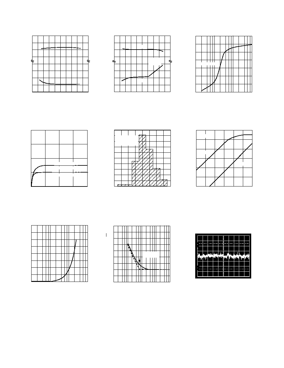
SUPPLY VOLTAGE ≠
±
V
+V
S
≠1.5
≠V
S
0
25
5
10
15
20
≠0.5
≠1.0
+1.5
+0.5
+1.0
+ V
OUT
≠ V
OUT
OUTPUT VOLTAGE SWING ≠
±
V
(REFERRED TO SUPPLY VOLTAGES)
R
L
= 2k
@ +25
∞
C
Figure 2. Output Voltage Swing
vs. Supply Voltage
OFFSET VOLTAGE DRIFT ≠ µV/
∞
C
NUMBER OF UNITS
100
70
20
≠0.4 ≠0.3
0.4
≠0.2 ≠0.1
0
0.1
0.2
0.3
90
80
50
30
60
40
10
0
256 UNITS
TESTED
≠ 55
∞
C TO +125
∞
C
Figure 5. Typical Distribution of
Offset Voltage Drift
FREQUENCY ≠ Hz
45
40
0
0.01
0.1
100
1
10
35
30
25
20
15
10
5
INPUT VOLTAGE NOISE ≠ nV/
Hz
I/F CORNER
0.7Hz
Figure 8. Input Noise Spectral
Density
LOAD RESISTANCE ≠
OUTPUT VOLTAGE ≠ V p -p
35
15
0
10
100
10k
1k
10
25
20
30
5
±
15V SUPPLIES
Figure 3. Output Voltage Swing
vs. Load Resistance
FREQUENCY ≠ Hz
OUTPUT IMPEDANCE ≠
100
0.0001
0.1
100k
1
10
100
1k
10k
10
1
0.1
0.001
0.01
I
O
= 1mA
A
V
= +1000
A
V
= +1
Figure 6. Output Impedance vs.
Frequency
10
0%
100
90
TIME ≠ 1sec/Div
VOLTAGE NOISE ≠ 100nV/Div
Figure 9. 0.1 Hz to 10 Hz Voltage
Noise
SUPPLY VOLTAGE ≠
±
V
+V
S
≠1.5
≠0.5
≠1.0
≠V
S
+1.5
+0.5
+1.0
0
25
5
10
15
20
+V
≠V
COMMOM-MODE VOLTAGE LIMIT ≠ V
(REFERRED TO SUPPLY VOLTAGES)
Figure 1. Input Common-Mode
Range vs. Supply Voltage
TIME AFTER POWER ON ≠ Minutes
CHANGE IN OFFSET ≠ µV
4
0
0
4
1
2
3
3
2
1
DUAL-IN-LINE PACKAGE
PLASTIC (N) or CERDIP (Q)
METAL CAN (H) PACKAGE
Figure 4. Offset Voltage Warm-Up
Drift
DIFFERENTIAL VOLTAGE ≠
±
V
40
30
0
0
1
100
10
20
10
INVERTING OR
NONINVERTING INPUT CURRENT ≠ mA
Figure 7. Input Current vs.
Differential Input Voltage
AD707
REV. B
≠5≠
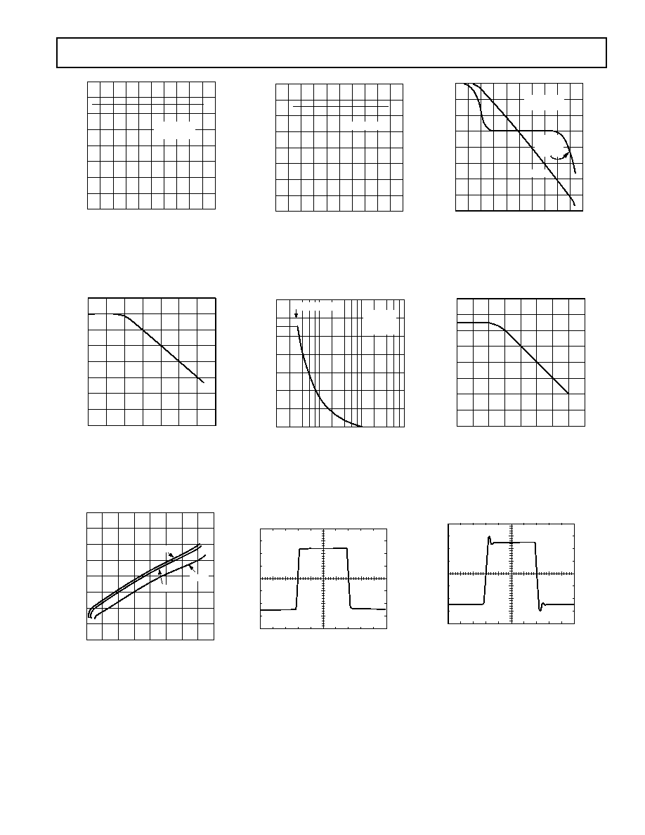
TEMPERATURE ≠
∞
C
16
10
0
≠60 ≠40
140
≠20
0
20
40
60
80 100 120
14
12
6
2
8
4
OPEN-LOOP GAIN ≠
V/µV
R
L
=
1k
V
OUT
=
±
10V
Figure 10. Open-Loop Gain vs.
Temperature
FREQUENCY ≠ Hz
COMMON-MODE REJECTION ≠ dB
160
0
0.1
1
10
100
1k
10k
100k
1M
140
100
80
60
20
120
40
Figure 13. Common-Mode
Rejection vs. Frequency
SUPPLY VOLTAGE ≠
±
V
SUPPLY CURRENT ≠ mA
4
0
0
3
24
6
9
12
15
18
21
2
1
3
+125
∞
C
+25
∞
C
≠55
∞
C
Figure 16. Supply Current vs.
Supply Voltage
SUPPLY VOLTAGE ≠ V
OPEN-LOOP GAIN ≠
V/µV
16
10
0
0
25
5
10
15
20
14
12
6
2
8
4
R
LOAD
= 1k
Figure 11. Open-Loop Gain vs.
Supply Voltage
FREQUENCY ≠ Hz
OUTPUT VOLTAGE ≠ V p-p
35
15
0
1k
10k
1M
100k
10
25
20
30
5
F
MAX
= 3kHz
R
L
= 2k
+25
∞
C
V
S
=
±
15V
Figure 14. Large Signal Frequency
Response
20mV/DIV
CH1
TIME ≠ 2µs/DIV
Figure 17. Small Signal Transient
Response; A
V
= +1, R
L
= 2 k
,
C
L
= 50 pF
FREQUENCY ≠ Hz
OPEN-LOOP GAIN ≠
V/µV
140
80
0
0.01 0.1
1
10 100 1k 10k 100k 1M 10M
120
100
40
10
60
20
PHASE ≠ Degrees
30
180
0
90
150
60
120
R
L
= 2k
C
L
= 1000pF
PHASE
MARGIN
=58
∞
GAIN
Figure 12. Open-Loop Gain and
Phase vs. Frequency
FREQUENCY ≠ Hz
POWER SUPPLY REJECTION ≠ dB
160
0
0.001 0.01
100k
0.1
1
10
100
1k
10k
140
80
60
40
20
120
100
Figure 15. Power Supply Rejection
vs. Frequency
20mV/DIV
CH1
TIME ≠ 2µs/DIV
Figure 18. Small Signal Transient
Response; A
V
= +1, R
L
= 2 k
,
C
L
= 1000 pF