 | –≠–ª–µ–∫—Ç—Ä–æ–Ω–Ω—ã–π –∫–æ–º–ø–æ–Ω–µ–Ω—Ç: AD708 | –°–∫–∞—á–∞—Ç—å:  PDF PDF  ZIP ZIP |
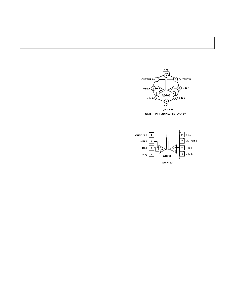
CONNECTION DIAGRAMS
TO-99 (H) Package
Plastic (N ), and Cerdip (Q) Packages
REV. B
Information furnished by Analog Devices is believed to be accurate and
reliable. However, no responsibility is assumed by Analog Devices for its
use, nor for any infringements of patents or other rights of third parties
which may result from its use. No license is granted by implication or
otherwise under any patent or patent rights of Analog Devices.
a
Ultralow Offset Voltage
Dual Op Amp
AD708
One Technology Way, P.O. Box 9106, Norwood, MA 02062-9106, U.S.A.
Tel: 617/329-4700
Fax: 617/326-8703
FEATURES
Very High DC Precision
30 V max Offset Voltage
0.3 V/ C max Offset Voltage Drift
0.35 V p-p max Voltage Noise (0.1 Hz to 10 Hz)
5 Million V/V min Open Loop Gain
130 dB min CMRR
120 dB min PSRR
Matching Characteristics
30 V max Offset Voltage Match
0.3 V/ C max Offset Voltage Drift Match
130 dB min CMRR Match
Single Version: AD707
Available in 8-Pin Plastic Mini-DIP,
Hermetic Cerdip and TO-99 Metal Can
Packages, Chips and /883B Parts Available.
PRODUCT DESCRIPTION
The AD708 is a very high precision, dual monolithic operational
amplifier. Each amplifier individually offers excellent dc precision
with the best available max offset voltage and offset voltage drift
of any dual bipolar op amp. In addition, the matching specifica-
tions are the best available in any dual op amp.
The AD708 sets a new standards for dual precision op amps by
providing 5 V/
µ
V min open loop gain and guaranteed max input
voltage noise of 350 nV p-p (0.1 Hz to 10 Hz). All dc specifica-
tions show excellent stability over temperature, with offset
voltage drift typically 0.1
µ
V/
∞
C and input bias current drift of
25 pA/
∞
C max. Both CMRR (130 dB min) and PSRR (120 dB
min) are an order of magnitude improved over any available
single monolithic op amp except the AD707.
The AD708 is available in four performance grades. The
AD708J is rated over the commercial temperature range of 0
∞
C
to +70
∞
C and jis available in a plastic mini-DIP package. The
AD708A and AD708B are rated over the industrial temperature
range of ≠40
∞
C to +85
∞
C and are available in a cerdip and TO-
99 package. The AD708S is rated over the military temperature
range of ≠55
∞
C to +125
∞
C and is available in cerdip and TO-99
packages. Military versions are available processed to MIL-
STD-883B, Rev. C.
APPLICATION HIGHLIGHTS
1. The combination of outstanding matching and individual
specifications make the AD708 ideal for constructing high
gain, precision instrumentation amplifiers.
2. The low offset voltage drift and low noise of the AD708
allows the designer to amplify very small signals without
sacrificing overall system performance.
3. The AD708's 10 V/
µ
V typical open loop gain and 140 dB
common-mode rejection make it ideal for precision
applications.
4. Unmounted dice are available for hybrid circuit applications.
5. The AD708 is an improved replacement for the LT1002.

AD708≠SPECIFICATIONS
(@ +25 C and 15 V dc, unless otherwise noted)
≠2≠
REV. B
AD708J/A
AD708B
AD708S
Model
Conditions
Min
Typ
Max
Min
Typ
Max
Min
Typ
Max
Units
INPUT OFFSET VOLTAGE
1
30
100
5
50
5
30
µ
V
T
MIN
to T
MAX
50
150
15
65
15
50
µ
V
Drift
0.3
1.0
0.1
0.4
0.1
0.3
µ
V/
∞
C
Long Term Stability
0.3
0.3
0.3
µ
V/Month
INPUT BIAS CURRENT
1.0
2.5
0.5
1.0
0.5
1
nA
T
MIN
to T
MAX
2.0
4.0
1.0
2.0
1.0
4
nA
Average Drift
15
40
10
25
10
30
pA/
∞
C
OFFSET CURRENT
V
CM
= 0 V
0.5
2.0
0.1
1.0
0.1
1
nA
T
MIN
to T
MAX
2.0
4.0
0.2
1.5
0.2
1.5
nA
Average Drift
2
60
1
25
1
25
pA/
∞
C
MATCHING CHARACTERISTICS
2
Offset Voltage
80
50
30
µ
V
T
MIN
to T
MAX
150
75
50
µ
V
Offset Voltage Drift
1.0
0.4
0.3
µ
V/
∞
C
Input Bias Current
4.0
1.0
1.0
nA
T
MIN
to T
MAX
5.0
2.0
2.0
nA
Common-Mode Rejection
120
140
130
140
130
140
dB
T
MIN
to T
MAX
110
130
130
dB
Power Supply Rejection
110
120
120
dB
T
MIN
to T
MAX
110
120
120
dB
Channel Separation
135
140
140
dB
INPUT VOLTAGE NOISE
0.1 Hz to 10 Hz
0.23
0.6
0.23
0.6
0.23
0.35
µ
V p-p
f = 10 Hz
10.3
18
10.3
12
10.3
12
nV/
Hz
f = 100 Hz
10.0
13.0
10.0
11.0
10.0
11
nV/
Hz
f = 1 kHz
9.6
11.0
9.6
11.0
9.6
11
nV/
Hz
INPUT CURRENT NOISE
0.1 Hz to 10 Hz
14
35
14
35
14
35
pA p-p
f = 10 Hz
0.32
0.9
0.32
0.8
0.32
0.8
pA/
Hz
f = 100 Hz
0.14
0.27
0.14
0.23
0.14
0.23
pA/
Hz
f = 1 kHz
0.12
0.18
0.12
0.17
0.12
0.17
pA/
Hz
COMMON-MODE
REJECTION RATIO
V
CM
=
±
13 V
120
140
130
140
130
140
dB
T
MIN
to T
MAX
120
140
130
140
130
140
dB
OPEN-LOOP GAIN
V
O
=
±
10 V
R
LOAD
2 k
3
10
5
10
4
10
V/
µ
V
T
MIN
to T
MAX
3
10
5
10
4
7
V/
µ
V
POWER SUPPLY
REJECTION RATIO
V
S
=
±
3 V to
±
18 V
110
130
120
130
120
130
dB
T
MIN
to T
MAX
110
130
120
130
120
130
dB
FREQUENCY RESPONSE
Closed Loop Bandwidth
0.5
0.9
0.5
0.9
0.5
0.9
MHz
Slew Rate
0.15
0.3
0.15
0.3
0.15
0.3
V/
µ
s
INPUT RESISTANCE
Differential
60
200
200
M
Common Mode
200
400
400
G
OUTPUT VOLTAGE
R
LOAD
10 k
13.5
14
13.5
14.0
13.5
14
±
V
R
LOAD
2 k
12.5
13.0
12.5
13.0
12.5
13
±
V
R
LOAD
1 k
12.0
12.5
12.0
12.5
12.0
12.5
±
V
R
LOAD
2 k
T
MIN
to T
MAX
12.0
13.0
12.0
13.0
12.0
13
±
V
OPEN-LOOP OUTPUT
RESISTANCE
60
60
60
AD708J/A
AD708B
AD708S
Model
Conditions
Min
Typ
Max
Min
Typ
Max
Min
Typ
Max
Units
POWER SUPPLY
Quiescent Current
4.5
5.5
4.5
5.5
4.5
5.5
mA
Power Consumption
V
S
=
±
15 V
No Load
135
165
135
165
135
165
mW
V
S
=
±
3 V
12
18
12
18
12
18
mW
Operating Range
±
3
±
18
±
3
±
18
±
3
±
18
V
NOTES
1
Input offset voltage specifications are guaranteed after 5 minutes of operation at T
A
= +25
∞
C.
2
Matching is defined as the difference between parameters of the two amplifiers.
All min and max specifications are guaranteed. Specifications in boldface are tested on all production units at final electrical test. Results from those tests are used to
calculate outgoing quality levels.
Specifications subject to change without notice.
ABSOLUTE MAXIMUM RATINGS
1
Supply Voltage . . . . . . . . . . . . . . . . . . . . . . . . . . . . . . . .
±
22 V
Internal Power Dissipation
2
Input Voltage
3
. . . . . . . . . . . . . . . . . . . . . . . . . . . . . . . . .
±
V
S
Output Short Circuit Duration . . . . . . . . . . . . . . . . Indefinite
Differential Input Voltage . . . . . . . . . . . . . . . . . . +V
S
and ≠V
S
Storage Temperature Range (Q, H) . . . . . . . ≠65
∞
C to +150
∞
C
Storage Temperature Range (N) . . . . . . . . . ≠65
∞
C to +125
∞
C
Lead Temperature Range (Soldering 60 sec) . . . . . . . . +300
∞
C
NOTES
1
Stresses above those listed under "Absolute Maximum Ratings" may cause
permanent damage to the device. This is a stress rating only and functional
operation of the device at these or any other conditions above those indicated in
the operational section of this specification is not implied. Exposure to absolute
maximum rating conditions for extended periods may affect device reliability.
2
Thermal Characteristics
8-Pin Plastic Package:
JC
= 33
∞
C/Watt,
JA
= 100
∞
C/Watt
8-Pin Cerdip package:
JC
= 30
∞
C/Watt,
JA
= 110
∞
C/Watt
8-Pin Metal Can Package:
JC
= 65
∞
C/Watt,
JA
= 150
∞
C/Watt.
3
For supply voltages less than
±
22 V, the absolute maximum input voltage is
equal to the supply voltage.
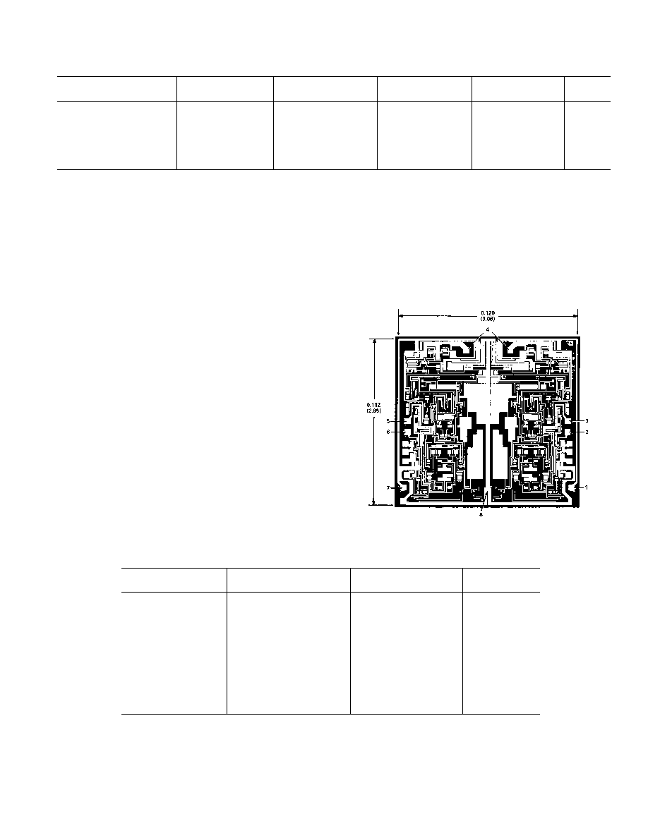
METALIZATION PHOTOGRAPH
Dimensions shown in inches and (mm).
Contact factory for latest dimensions.
REV. B
≠3≠
AD708
ORDERING GUIDE
Temperature
Package
Package
Model
Range
Description
Option*
AD708JN
0
∞
C to +70
∞
C
8-Pin Plastic DIP
N-8
AD708AQ
≠40
∞
C to +85
∞
C
8-Pin Cerdip
Q-8
AD708BQ
≠40
∞
C to +85
∞
C
8-Pin Cerdip
Q-8
AD708SQ
≠55
∞
C to +125
∞
C
8-Pin Cerdip
Q-8
AD708AH
≠40
∞
C to +85
∞
C
8-Pin Header
H-08A
AD708BH
≠40
∞
C to +85
∞
C
8-Pin Header
H-08A
AD708SH
≠55
∞
C to +125
∞
C
8-Pin Header
H-08A
AD708SH/883B
≠55
∞
C to +125
∞
C
8-Pin Header
H-08A
AD708J Grade Chips
0
∞
C to +70
∞
C
Die
AD708S Grade Chips
≠55
∞
C to +125
∞
C
Die
*N = Plastic DIP; Q = Cerdip; H = Hermetic Metal Can.
REV. B
≠4≠
(V
S
= 15 V and T
A
= +25 C unless otherwise noted)
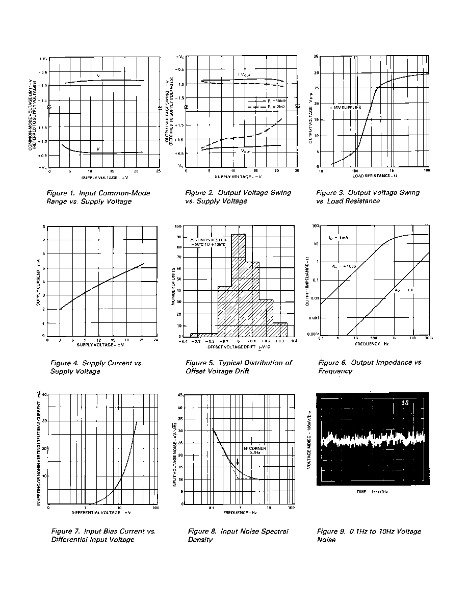
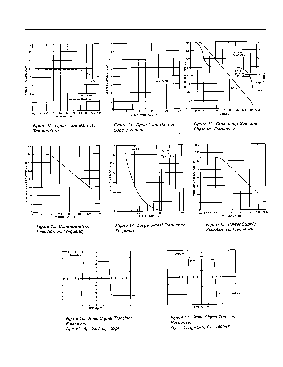
AD708≠Typical Characteristics
AD708
REV. B
≠5≠
REV. B
≠6≠
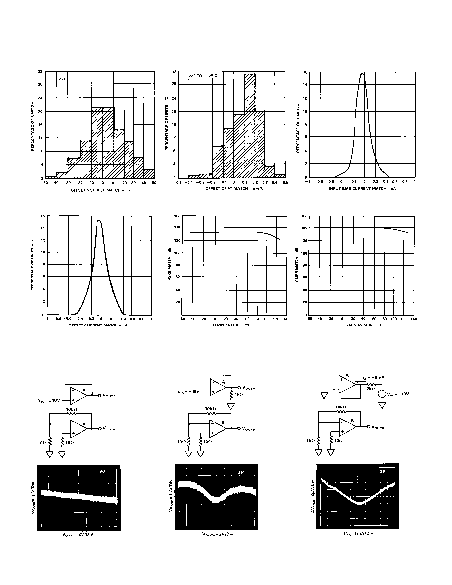
Figure 24. Crosstalk with No Load
Figure 26. Crosstalk under Forced
Source and Sink Conditions
Figure 25. Crosstalk with 2 k
Load
Figure 20. Typical Distribution of Input
Bias Current Match
Crosstalk from Thermal Effects of Power Dissipation
AD708≠Matching Characteristics
Figure 19. Typical Distribution of Offset
Voltage Drift Match
Figure 18. Typical Distribution of Offset
Voltage Match
Figure 21. Typical Distribution of Input
Offset Current Match
Figure 22. PSRR Match vs.
Temperature
Figure 23. CMRR Match vs.
Temperature
AD708
REV. B
≠7≠
CROSSTALK PERFORMANCE OF THE AD708
The AD708 exhibits very low crosstalk as shown in Figures 24,
25 and 26. Figure 24 shows the offset voltage induced in side B
of the AD708 when side A's output is moving slowly (0.2 Hz)
from ≠10 V to +10 V under no load. This is the least stressful
situation to the part since the overall power in the chip does not
change; only the location of the power in the output devices
changes. Figure 25 shows side B's input offset voltage change
when side A is driving a 2 k
load. Here the power is being
changed in the chip with the maximum power change occurring
at
±
7.5 V. Figure 26 shows crosstalk under the most severe
conditions. Side A is connected as a follower with 0 V input,
and is now forced to sink and source
±
5 mA of output current
(Power = (30 V) (5 mA) = 150 mW). Even this large change in
power causes only an 8
µ
V (linear) change in side B's input
offset voltage.
OPERATION WITH A GAIN OF ≠100
To show the outstanding dc precision of the AD708 in real
application, Table I shows an error budget calculation for a gain
of ≠100 configuration shown in Figure 27.
Table I.
Maximum Error Contribution
A
V
= 100 (S Grade)
Error Sources
(Full Scale: V
OUT
= 10 V, V
IN
= 100 mV)
V
OS
30
µ
V/100 mV
= 300 ppm
I
OS
(100 k
)(1 nA)/10 V
= 10 ppm
Gain (2 k
load)
10 V/(5*10
6
))/100 mV
= 20 ppm
Noise
0.35
µ
V/100 mV
= 4 ppm
V
OS
Drift
(0.3
µ
V/
∞
C)/100 mV
= 3 ppm/
∞
C
= 334 ppm
+3 ppm/
∞
C
Total Unadjusted
Error
@ 25
∞
C
= 334 ppm > 11 Bits
≠55
∞
C to +125
∞
C
= 634 ppm > 10 Bits
With Offset
Calibrated Out
@ 25
∞
C
= 34 ppm > 14 Bits
≠55
∞
C to +125
∞
C
= 334 ppm > 11 Bits
Figure 27. Gain of ≠100 Configuration
This error budget assumes no error in the resistor ratio and no
error from power supply variation (the 120 dB minimum PSRR
of the AD708S makes this a good assumption). The external
resistors can cause gain error from mismatch and drift over
temperature.
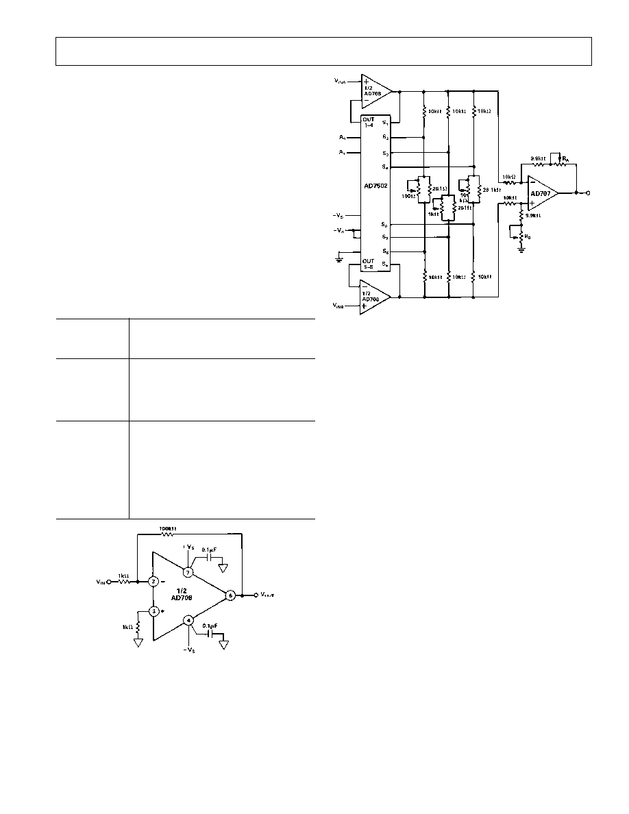
High Precision Programmable Gain Amplifier
The three op amp programmable gain amplifier shown in Figure
28 takes advantage of the outstanding matching characteristics of
the AD708 to achieve high dc precision. The gains of the circuit
Figure 28. Precision PGA
are controlled by the select lines, A0 and A1 of the AD7502
multiplexer, and are 1, 10, 100 and 1000 in this design.
The input stage attains very high dc precision due to the 30
µ
V
maximum offset voltage match of the AD708S and the 1 nA
maximum input bias current match. The accuracy is maintained
over temperature because of the ultralow drift performance of
the AD708. The output stage uses an AD707J and well matched
resistors configured as a precision subtracter.
To achieve 0.1% gain accuracy, along with high common-mode
rejection, the circuit should be trimmed as follows:
To maximize common-mode rejection:
1. Set the select lines for Gain = 1 and ground V
INB
.
2. Apply a precision dc voltage to V
INA
and trim R
A
until
V
O
= ≠V
INA
to the required precision.
3. Next connect V
INB
to V
INA
and apply an input voltage equal
to the full-scale common-mode expected.
4. Trim R
B
until V
O
= 0 V.
To minimize gain errors:
1. Select Gain = 10 with the control lines and apply a differential
input voltage.
2. Adjust the 100
potentiometer such that V
O
= 10 V
IN
(adjust
V
IN
magnitude as necessary).
3. Repeat for Gain = 100 and Gain = 1000, adjusting 1 k
and
10 k
potentiometers, respectively.
The design shown should allow for 0.1% gain accuracy and
0.1
µ
V/V common-mode rejection when
±
1% resistors and
±
5%
potentiometers are used.
BRIDGE SIGNAL CONDITIONER
The AD708 can be used in the circuit in Figure 29 to produce
an accurate and inexpensive dynamic bridge conditioner. The
low offset voltage match and low offset voltage drift match of
the AD708 combine to achieve circuit performance better than
all but the best instrumentation amplifiers. The AD708's out-
standing specs: open loop gain, input offset currents and low
input bias currents, do not limit circuit accuracy.

AD708
REV. B
≠8≠
C1252a≠10≠2/91
PRINTED IN U.S.A.
As configured, the circuit only requires a gain resistor, R
G
, of
suitable accuracy and a stable, accurate voltage reference. The
transfer function is:
V
O
= V
REF
[
R/(R+
R)][R
G
/R]
and the only significant errors due to the AD708S are:
V
OS
out = (V
OS
match)(2R
G
/R) = 30 mV
V
OS
out(T) = (V
OS
drift)(2R
G
/R) = 0.3 mV/
∞
C
To achieve high accuracy, the resistor R
G
should be 0.1% or
better and have a low drift coefficient.
Figure 29. Bridge Signal Conditioning Circuit
Figure 30. Precision Absolute Value Circuit
PRECISION ABSOLUTE VALUE CIRCUIT
The AD708 is ideally suited to the precision absolute value
circuit shown in Figure 30. The low offset voltage match of the
AD708 enables this circuit to accurately resolve the input signal.
In addition, the tight offset voltage drift match maintains the
resolution of the circuit over the full military temperature range.
The AD708's high dc open loop gain and exceptional gain
linearity allows the circuit to perform well at both large and
small signal levels.
In this circuit, the only significant dc errors are due to the offset
voltage of the two ampliliers, the input offset current match of
the amplifiers, and the mismatch of the resistors. Errors associ-
ated with the AD708S contribute less than 0.001% error over
≠55
∞
C to +125
∞
C.
Maximum error at 25
∞
C
30
µ
V
+
10 k
(
)
1nA
( )
10V
=
40
µ
V /10V
=
4 ppm Maximum
error at +125
∞
C or ≠55
∞
C
50
µ
V
+
2 nA
( )
10 k
(
)
10V
=
7 ppm @
+
125
∞
C
Figure 31 shows V
OUT
vs. V
IN
for this circuit with a
±
3 mV
input signal at 0.05 Hz. Note that the circuit exhibits very low
offset at the zero crossing. This circuit can also produce V
OUT
=
≠|V
IN
| by reversing the polarity of the two diodes.
Figure 31. Absolute Value Circuit Performance
(Input Signal = 0.05 Hz)
SELECTION OF PASSIVE COMPONENTS
To takc full advantagc of thc high precision and low drift
characteristics of the AD708, high quality passive components
must be used. Discrete resistors and resistor networks with
temperature coefficients of less than 10 ppm/
∞
C are available
from Vishay, Caddock, PRP and others.
OUTLINE DIMENSIONS
Dimensions shown in inches and (mm).
TO-99 (H) Package
Cerdip (Q) Package
Mini-DIP (N) Package