 | ÐлекÑÑоннÑй компоненÑ: AD7112B | СкаÑаÑÑ:  PDF PDF  ZIP ZIP |
AD7112* LC2MOS LOGDAC Dual Logarithmic D/A Converter
REV. 0
Information furnished by Analog Devices is believed to be accurate and
reliable. However, no responsibility is assumed by Analog Devices for its
use, nor for any infringements of patents or other rights of third parties
which may result from its use. No license is granted by implication or
otherwise under any patent or patent rights of Analog Devices.
a
LC
2
MOS LOGDAC
Dual Logarithmic D/A Converter
AD7112*
One Technology Way, P.O. Box 9106, Norwood, MA 02062-9106, U.S.A.
Tel: 617/329-4700
Fax: 617/326-8703
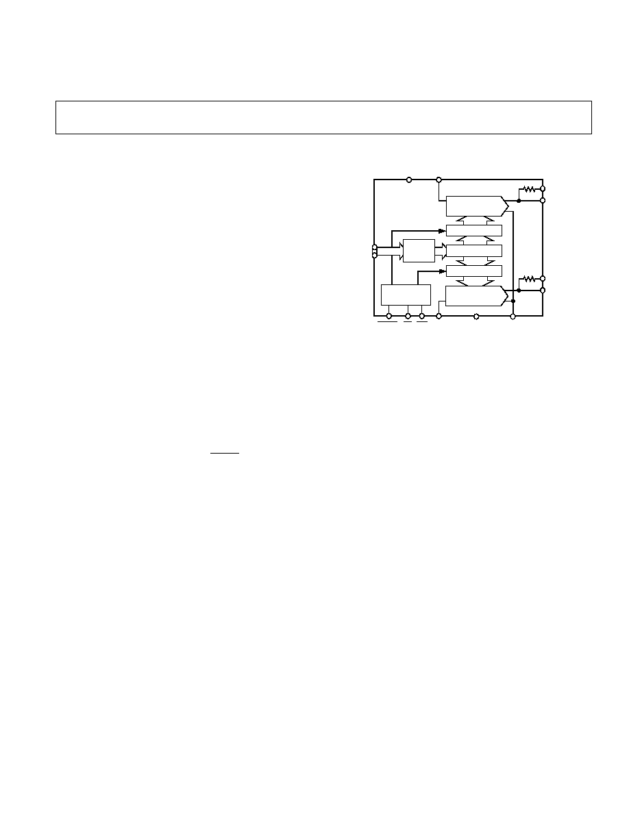
FUNCTIONAL BLOCK DIAGRAM
17-BIT DAC A
AD7112
OUT A
AGND
DGND
CS
WR
17-BIT LATCH
17
17-BIT LATCH
17-BIT DAC B
R
FB
A
OUT B
R
FB
B
DECODE LOGIC
V
IN
B
V
IN
A
DAC A/
DAC B
CONTROL
LOGIC
8-BIT
BUFFER
DB0
DB7
V
DD
FEATURES
Dynamic Range: 88.5 dB
Resolution: 0.375 dB
On-Chip Data Latches for Both DACs
Four-Quadrant Multiplication
+5 V Operation
Pin Compatible with AD7528
Low Power
APPLICATIONS
Audio Attenuators
Sonar Systems
Function Generators
GENERAL DESCRIPTION
The LOGDAC® AD7112 is a monolithic dual multiplying D/A
converter featuring wide dynamic range and excellent DAC-to-
DAC matching. Both DACs can attenuate an analog input sig-
nal over the range 0 dB to 88.5 dB in 0.375 dB steps. It is
available in skinny 0.3" wide 20-pin DIPs and in 20-terminal
surface mount packages.
The degree of attenuation in either channel is determined by the
8-bit word applied to the onboard decode logic. This 8-bit word
is decoded into a 17-bit word which is then loaded into one of
the 17-bit data latches, determined by DACA/DACB. The fine
step resolution over the entire dynamic range is due to the use of
these 17-bit DACs.
The AD7112 is easily interfaced to a standard 8-bit MPU bus
via an 8-bit data port and standard microprocessor control lines.
It should be noted that the AD7112 is exactly pin-compatible
with the AD7528, an industry standard dual 8-bit multiplying
DAC. This allows an easy upgrading of existing AD7528 de-
signs which would benefit both from the wider dynamic range
and the finer step resolution offered by the AD7112.
The AD7112 is fabricated in Linear Compatible CMOS
(LC
2
MOS), an advanced, mixed technology process that com-
bines precision bipolar circuits with low power CMOS logic.
*Protected by U.S. Patent No. 4521764.
LOGDAC is a registered trademark of Analog Devices, Inc.
PRODUCT HIGHLIGHTS
1. DAC-to-DAC Matching: Since both of the AD7112 DACs
are fabricated at the same time on the same chip, precise
matching and tracking between the two DACs is inherent.
2. Small Package: The AD7112 is available in a 20-pin DIP
and a 20-terminal SOIC package.
3. Fast Microprocessor Interface: The AD7112 has bus inter-
face timing compatible with all modern microprocessors.

REV. 0
2
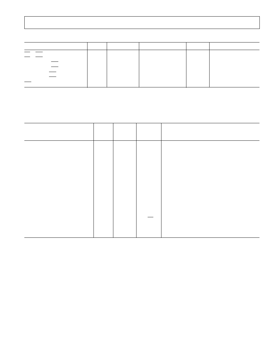
AD7112SPECIFICATIONS
(V
DD
= +5 V 5%; OUT A = OUT B = AGND = DGND = 0 V; V
IN
A = V
IN
B = 10 V.
Output amplifier AD712 except where noted. All specifications T
MIN
to T
MAX
unless otherwise noted.)
C Version
1
B Version
T
A
=
T
A
=
T
A
=
T
A
=
Parameter
+25 C
T
MIN
, T
MAX
+25 C
T
MIN
, T
MAX
Units
Conditions/Comments
ACCURACY
Resolution
0.375
0.375
0.375
0.375
dB
Accuracy Relative to
Guaranteed Attenuation
0 dB Attenuation
Ranges for Specified Step Sizes.
0.375 dB Steps:
Accuracy
±
0.17 dB
0 to 36
0 to 36
0 to 30
0 to 30
dB min
Monotonic
0 to 54
0 to 54
0 to 48
0 to 48
dB min
0.75 dB Steps:
Accuracy
±
0.35 dB
0 to 48
0 to 42
0 to 42
0 to 36
dB min
Monotonic
0 to 72
0 to 66
0 to 72
0 to 60
dB min
1.5 dB Steps:
Accuracy
±
0.7 dB
0 to 54
0 to 48
0 to 48
0 to 42
dB min
Monotonic
Full Range 0 to 78
0 to 85.5
0 to 72
dB min
Full Range Is 0 dB to 88.5 dB.
3.0 dB Steps:
Accuracy
±
1.4 dB
0 to 66
0 to 54
0 to 60
0 to 48
dB min
Monotonic
Full Range Full Range
Full Range Full Range
dB min
6.0 dB Steps:
Accuracy
±
2.7 dB
0 to 72
0 to 60
0 to 60
0 to 60
dB min
Monotonic
Full Range Full Range
Full Range Full Range
dB min
Gain Error
±
0.1
±
0.15
±
0.15
±
0.2
dB max
Measured Using R
FB
A,
R
FB
B. Both DAC Registers
Loaded With All 0s.
Output Leakage Current
OUT A, OUT B
±
50
±
400
±
50
±
400
nA max
Input Resistance,
V
IN
A, V
IN
B
9/15
9/15
9/15
9/15
k
min/max Typically 12 k
.
Input Resistance Match
±
1
±
1
±
2
±
2
% max
Feedback Resistance,
R
FB
A, R
FB
B
9.3/15.7
9.3/15.7
9.3/15.7
9.3/15.7
k
min/max
LOGIC INPUTS
CS
, WR,
DAC A
/DAC B,
DB0DB7
Input Low Voltage, V
INL
0.8
0.8
0.8
0.8
V max
Input High Voltage, V
INH
2.4
2.4
2.4
2.4
V min
Input Leakage Current
±
1
±
10
±
1
±
10
µ
A max
Input Capacitance
2
10
10
10
10
pF max
POWER REQUIREMENTS
V
DD
, Range
3
4.75/5.25
4.75/5.25
4.75/5.25
4.75/5.25
V min/max
For Specified Performance.
2
2
2
2
mA max
Logic Inputs = V
IL
or V
IH
2
2
2
2
mA max
Logic Inputs = 0 V or V
DD
NOTES
l
Temperature range as follows: B, C Versions: 40
°
C to +85
°
C.
2
Guaranteed by design, not production tested.
3
The part will function with V
DD
= 5 V
±
10% with degraded performance.
Specifications subject to change without notice.
AD7112
REV. 0
3
TIMING SPECIFICATIONS
1
Parameter
T
A
= +25 C
T
A
= 40 C to +85 C
Units
Conditions/Comments
CS
to WR Setup Time
t
CS
0
0
ns min
See Figure 3.
CS
to WR Hold Time
t
CH
0
0
ns min
DAC Select to WR Setup Time
t
AS
4
4
ns min
DAC Select to WR Hold Time
t
AH
0
0
ns min
Data Valid to WR Setup Time
t
DS
55
55
ns min
Data Valid to WR Hold Time
t
DH
10
10
ns min
WR
Pulse Width
t
WR
53
53
ns min
NOTES
1
Timing specifications guaranteed by design not production tested. All input signals are specified with tr = tf = 5 ns (10% to 90% of 5 V) and timed from a voltage
level of 1.6 V.
Specifications subject to change without notice.
AC PERFORMANCE CHARACTERISTICS
1
T
A
=
T
A
=
40 C to
Parameter
+25 C
+85 C
Units
Conditions/Comments
DC Supply Rejection
Gain/
V
DD
0.001
0.005
dB/% max
V
DD
=
±
5%. Input Code = 00000000
Digital-to-Analog Glitch Impulse
10
10
nV s typ
Measured with AD843 as output amplifier for input
code transition 10000000 to 00000000.
Output Capacitance, C
OUT A
, C
OUT B
50
50
pF max
AC Feedthrough
V
IN
A to OUT A
94
90
dB max
V
IN
A, V
IN
B = 6 V rms at 1 kHz. DAC
Registers loaded with all 1s.
V
IN
B to OUT B
94
90
dB max
Channel-to-Channel Isolation
V
IN
A to OUT B
87
87
dB typ
V
IN
A = 6 V rms at 10 kHz sine wave,
V
IN
B = 0 V. DAC Registers loaded with all 0s.
V
IN
B to OUT A
87
87
dB typ
V
IN
B = 6 V rms at 10 kHz sine wave,
V
IN
A = 0 V. DAC Registers loaded with all 0s.
Digital Feedthrough
1
1
nV s typ
Measured with input code transitions of all 0s to all 1s.
Output Noise Voltage Density
(30 Hz to 50 kHz)
15
15
nV/
Hz
typ
Measured between R
FB
A and OUT A or between
R
FB
B and OUT B.
Total Harmonic Distortion
91
91
dB typ
V
IN
A = V
IN
B = 6 V rms at 1 kHz. DAC
Registers loaded with all 0s.
NOTES
1
Guaranteed by design, not production tested.
Specifications subject to change without notice.
(V
DD
= +5 V 5%; 0UT A = OUT B = AGND = DGND = O V; V
IN
A = V
IN
B = 10 V)
(V
DD
= +5 V 5%; 0UT A = OUT B = AGND = DGND = 0 V; V
IN
A =
V
IN
B = 10 V. Output amplifier AD712 except where noted.)
AD7112
REV. 0
4
ABSOLUTE MAXIMUM RATINGS*
V
DD
to AGND or DGND . . . . . . . . . . . . . . . . . . 0.3 V, +7 V
AGND to DGND . . . . . . . . . . . . . . . . . . 0.3 V, V
DD
+ 0.3 V
Digital Inputs to DGND . . . . . . . . . . . . . 0.3 V, V
DD
+ 0.3 V
OUT A, OUT B to AGND . . . . . . . . . . . 0.3 V, V
DD
+ 0.3 V
V
IN
A, V
IN
B to AGND . . . . . . . . . . . . . . . . . . . . . . . . .
±
25 V
V
RFB
A, V
RFB
B to AGND . . . . . . . . . . . . . . . . . . . . . . .
±
25 V
Operating Temperature Range
All Versions . . . . . . . . . . . . . . . . . . . . . . . . 40
°
C to +85
°
C
Junction Temperature . . . . . . . . . . . . . . . . . . . . . . . . +150
°
C
Storage Temperature . . . . . . . . . . . . . . . . . 65
°
C to +150
°
C
Power Dissipation, DIP . . . . . . . . . . . . . . . . . . . . . . . . . . 1 W
JA
, Thermal Impedance . . . . . . . . . . . . . . . . . . . . . 102
°
C/W
Lead Temperature (Soldering, 10 secs) . . . . . . . . . . . +300
°
C
Power Dissipation, SOIC . . . . . . . . . . . . . . . . . . . . . . . . . 1 W
JA
, Thermal Impedance . . . . . . . . . . . . . . . . . . . . . . 75
°
C/W
Lead Temperature (Soldering)
Vapor Phase (60 secs) . . . . . . . . . . . . . . . . . . . . . . . . 215
°
C
Infrared (15 secs) . . . . . . . . . . . . . . . . . . . . . . . . . . . . 220
°
C
*Stresses above those listed under "Absolute Maximum Ratings" may cause
permanent damage to the device. This is a stress rating only and functional
operation of the device at these or any other conditions above those listed in the
operational sections of this specification is not implied. Exposure to absolute
maximum rating conditions for extended periods may affect device reliability. Only
one Absolute Maximum Rating may be applied at any one time.
WARNING!
ESD SENSITIVE DEVICE
CAUTION
ESD (electrostatic discharge) sensitive device. Electrostatic charges as high as 4000 V readily
accumulate on the human body and test equipment and can discharge without detection.
Although the AD7112 features proprietary ESD protection circuitry, permanent damage may
occur on devices subjected to high energy electrostatic discharges. Therefore, proper ESD
precautions are recommended to avoid performance degradation or loss of functionality.
TERMINOLOGY
RESOLUTION: Nominal change in attenuation when moving
between two adjacent codes.
MONOTONICITY: The device is monotonic if the analog out-
put decreases or remains constant as the wdigital code in-
creases.
FEEDTHROUGH ERROR: That portion of the input signal
which reaches the output when all digital inputs are high.
OUTPUT CAPACITANCE: Capacitance from OUT A or
OUT B to ground.
GAIN ERROR: Gain error results from a mismatch between
R
FB
(the feedback resistance) and the R-2R ladder resistance.
Its effect in a LOGDAC is to produce a constant additive at-
tenuation error in dB over the whole range of the DAC.
ACCURACY: The difference (measured in dB) between the
ideal transfer function as listed in Table I and the actual trans-
fer function as measured with the device.
DIGITAL-TO-ANALOG GLITCH IMPULSE: The amount
of charge injected from the digital inputs to the analog output
when the inputs change state. This is normally specified as the
area of the glitch in either pA-s or nV-s depending on whether
the glitch is measured as a current or voltage signal. Glitch im-
pulse is measured with V
IN
= AGND.
ORDERING INFORMATION
Specified
Temperature
Accuracy
Package
Model
Range
Range
Option*
AD7112BN
40
°
C to +85
°
C
0 dB to 60 dB
N-20
AD7112CN
40
°
C to +85
°
C
0 dB to 72 dB
N-20
AD7112BR
40
°
C to +85
°
C
0 dB to 60 dB
R-20
AD7112CR
40
°
C to +85
°
C
0 dB to 72 dB
R-20
*N = Plastic DIP; R = SOIC.
PIN FUNCTION DESCRIPTION
Pin
Mnemonic
Description
1
AGND
Analog Ground.
2
OUT A
Current Output Terminal of DAC A.
3
R
FB
A
Feedback Resistor for DAC A.
4
V
IN
A
Reference Input to DAC A
5
DGND
Digital Ground.
6
DAC A
/
Selects Which DAC Can Accept Data from
DAC B
Input Port.
714 DB7DB0
8 Data Inputs.
15
CS
Chip Select Input, Active Low.
16
WR
Write Input, Active Low.
17
V
DD
Power Supply Input 5 V
±
5%.
18
V
IN
B
Reference Input to DAC B.
19
R
FB
B
Feedback Resistor for DAC B.
20
OUT B
Current Output Terminal of DAC B.
PIN CONFIGURATION
DIP/SOIC
AGND
OUT A
DGND
(MSB) DB7
DAC A/DAC B
DB6
DB5
DB4
R
FB
A
V
IN
A
OUT B
R
FB
B
V
IN
B
V
DD
DB0 (LSB)
DB1
DB2
DB3
1
2
3
4
5
6
7
8
9
10
20
19
18
17
16
15
14
13
12
11
TOP VIEW
(Not to Scale)
AD7112
WR
CS
AD7112
REV. 0
5
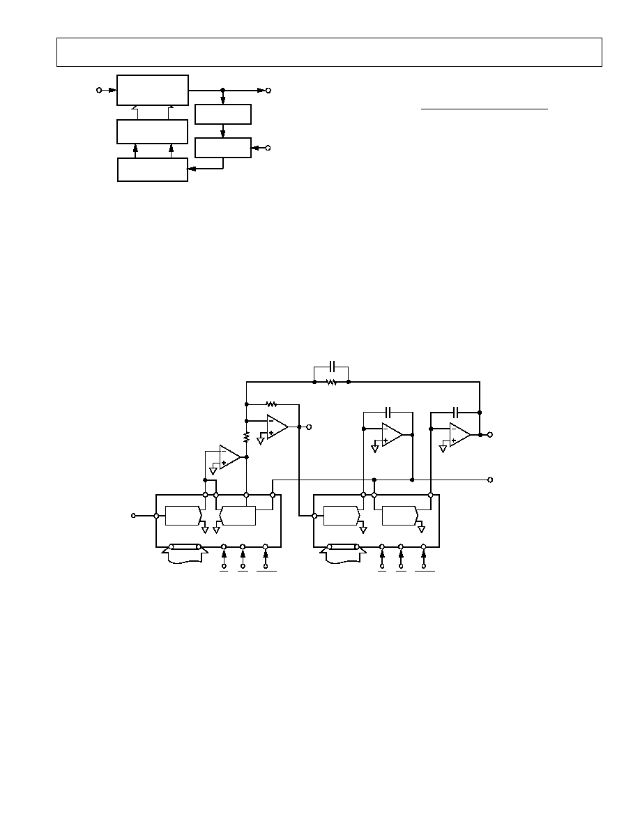
CIRCUIT DESCRIPTION
GENERAL CIRCUIT INFORMATION
The AD7112 consists of a dual 17-bit R-2R CMOS multiplying
D/A converter with extensive digital logic. Figure 1 shows a sim-
plified circuit of the D/A converter section of the AD7112. The
logic translates the 8-bit binary input into a 17-bit word which is
used to drive the D/A converter. Figure 2 shows a typical circuit
configuration for the AD7112.
The transfer function for the circuit of Figure 2 is given by:
V
O
=
V
IN
×
10 exp
0.375 N
20
or
V
O
V
IN
dB
=
0.375 N
where 0.375 is the step size (resolution ) in dB and N is the
input code in decimal for values 0 to 239. For 240
N
255
the output is zero. Table I gives the output attenuation relative
to 0 dB for all possible input codes.
R
2R
V
IN
A
R
R
2R
2R
2R
2R
R
R
FB
A
OUT A
AGND
S1
S2
S3
S17
Figure 1. Simplified D/A Circuit of 1/2 AD7112
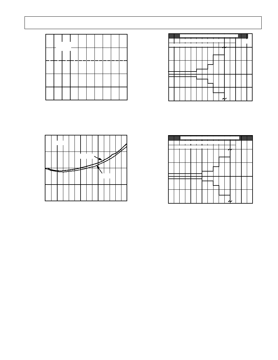
Figures 16 and 17 give a pictorial representation of the specified
accuracy and monotonic ranges for all grades of the AD7112.
High attenuation levels are specified with less accuracy than low
attenuation levels. The range of monotonic behavior depends
upon the attenuation step size used. To achieve monotonic op-
eration over the entire 88.5 dB range, it is necessary to select in-
put codes so that the attenuation step size at any point is
consistent with the step size guaranteed for monotonic opera-
tion at that point.
OUT A
AGND
DAC A
AD7112
DGND
CS
WR
R
FB
A
V
IN
A
DAC A/DAC B
V
DD
15
4
3
17
5
2
1
V
OUT
A1
C1
SIGNAL
GROUND
A1: 1/2 AD712
1/2 OP-275
6
16
NOTES
1. ONLY ONE DAC IS SHOWN FOR CLARITY.
2. DATA INPUT CONNECTIONS ARE OMITTED.
3. C1 PHASE COMPENSATION (515pF) MAY BE REQUIRED WHEN
USING HIGH SPEED AMPLIFIER.
Figure 2. Typical Circuit Configuration
Table I. Ideal Attenuation in dB vs. Input Code
D7D4
0000
0001
0010
0011
0100
0101
0110
0111
1000
1001
1010
1011
1100
1101
1110
1111
0000
0.000
0.375
0.750
1.125
1.500
1.875
2.250
2.625
3.000
3.375
3.750
4.125
4.500
4.875
5.250
5.625
0001
6.000
6.375
6.750
7.125
7.500
7.875
8.250
8.625
9.000
9.375
9.750
10.125
10.500
10.875
11.250
11.625
0010
12.000
12.375
12.750
13.125
13.500
13.875
14.250
14.625
15.000
15.375
15.750
16.125
16.500
16.875
17.250
17.625
0011
18.000
18.375
18.750
19.125
19.500
19.875
20.250
20.625
21.000
21.375
21.750
22.125
22.500
22.875
23.250
23.625
0100
24.000
24.375
24.750
25.125
25.500
25.875
26.250
26.625
27.000
27.375
27.750
28.125
28.500
28.875
29.250
29.625
0101
30.000
30.375
30.750
31.125
31.500
31.875
32.250
32.625
33.000
33.375
33.750
34.125
34.500
34.875
35.250
35.625
0110
36.000
36.375
36.750
37.125
37.500
37.875
38.250
38.625
39.000
39.375
39.750
40.125
40.500
40.875
41.250
41.625
0111
42.000
42.375
42.750
43.125
43.500
43.875
44.250
44.625
45.000
45.375
45.750
46.125
46.500
46.875
47.250
47.625
1000
48.000
48.375
48.750
49.125
49.500
49.875
50.250
50.625
51.000
51.375
51.750
52.125
52.500
52.875
53.250
53.625
1001
54.000
54.375
54.750
55.125
55.500
55.875
56.250
56.625
57.000
57.375
57.750
58.125
58.500
58.875
59.250
59.625
1010
60.000
60.375
60.750
61.125
61.500
61.875
62.250
62.625
63.000
63.375
63.750
64.125
64.500
64.875
65.250
65.625
1011
66.000
66.375
66.750
67.125
67.500
67.875
68.250
68.625
69.000
69.375
69.750
70.125
70.500
70.875
71.250
71.625
1100
72.000
72.375
72.750
73.125
73.500
73.875
74.250
74.625
75.000
75.375
75.750
76.125
76.500
76.875
77.250
77.625
1101
78.000
78.375
78.750
79.125
79.500
79.875
80.250
80.625
81.000
81.375
81.750
82.125
82.500
82.875
83.250
83.625
1110
84.000
84.375
84.750
85.125
85.500
85.875
86.250
86.625
87.000
87.375
87.750
88.125
88.500
88.875
89.250
89.625
1111
MUTE
MUTE
MUTE
MUTE
MUTE
MUTE
MUTE
MUTE
MUTE
MUTE
MUTE
MUTE
MUTE
MUTE
MUTE
MUTE
D3D0
AD7112
REV. 0
6
INTERFACE LOGIC INFORMATION
DAC Selection
Both DAC latches share a common 8-bit port. The control in-
put DAC A/DAC B selects which DAC can accept data from
the input port.
Mode Selection
Inputs CS and WR control the operating mode of the selected
DAC. See the Mode Selection Table below.
Write Mode
When CS and WR are both low the DAC is in the write mode.
The input data latches of the selected DAC are transparent and
its analog output responds to activity on DB0DB7.
Hold Mode
The selected DAC latch retains the data which was present on
DB0DB7 just prior to CS and WR assuming a high state. Both
analog outputs remain at the values corresponding to the data in
their respective latches.
Mode Selection Table
DACA
/
DAC B
CS
WR
DAC A
DAC B
L
L
L
WRITE
HOLD
H
L
L
HOLD
WRITE
X
H
X
HOLD
HOLD
X
X
H
HOLD
HOLD
L = Low State, V
IL
; H = High State, V
IH
; X = Don't Care.
t
AS
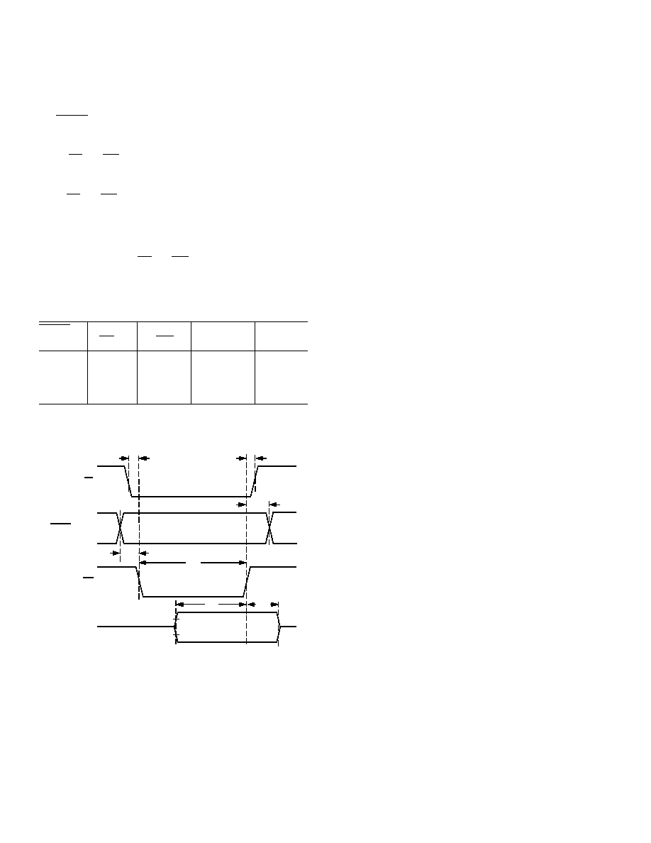
DAC A/DAC B
t
AH
t
WR
t
DS
V
IH
V
IL
t
DH
t
CS
t
CH
DB0DB7
CS
WR
NOTES
1. ALL INPUT SIGNAL RISE AND FALL TIMES MEASURED FROM
10% TO 90% OF V
DD
.
t
R
=
t
F = 20ns.
2. CONTROL TIMING MEASUREMENT REFERENCE LEVEL = (V
IH
+ V
IL
) / 2
Figure 3. Write Cycle Timing Diagram
DYNAMIC PERFORMANCE
The dynamic performance of the AD7112 will depend on the
gain and phase characteristics of the output amplifier, together
with the optimum choice of PC board layout and decoupling
components. Circuit layout is most important if the optimum
performance of the AD7112 is to be achieved. Most application
problems stem from either poor layout, grounding errors, or in-
appropriate choice of amplifier. Ensure that the layout of the
printed circuit board has the digital and analog lines separated
as much as possible. Take care not to run any digital track
alongside an analog signal track. Establish a single point analog
ground (star ground) separate from the logic system ground.
Place this ground as close as possible to the AD7112. Connect
all analog grounds to this star ground, and also connect the
AD7112 DGND to this ground. Do not connect any other digi-
tal grounds to this analog ground point. Low impedance analog
and digital power supply common returns are essential for low
noise and high performance of these converters, therefore the
foil width of these tracks should be as wide as possible. The use
of ground planes is recommended as this minimizes impedance
paths and also guards the analog circuitry from digital noise.
It is recommended that when using the AD7112 with a high
speed amplifier, a capacitor (C1) be connected in the feedback
path as shown in Figure 2. This capacitor which should be be-
tween 5 pF and 15 pF, compensates for the phase lag intro-
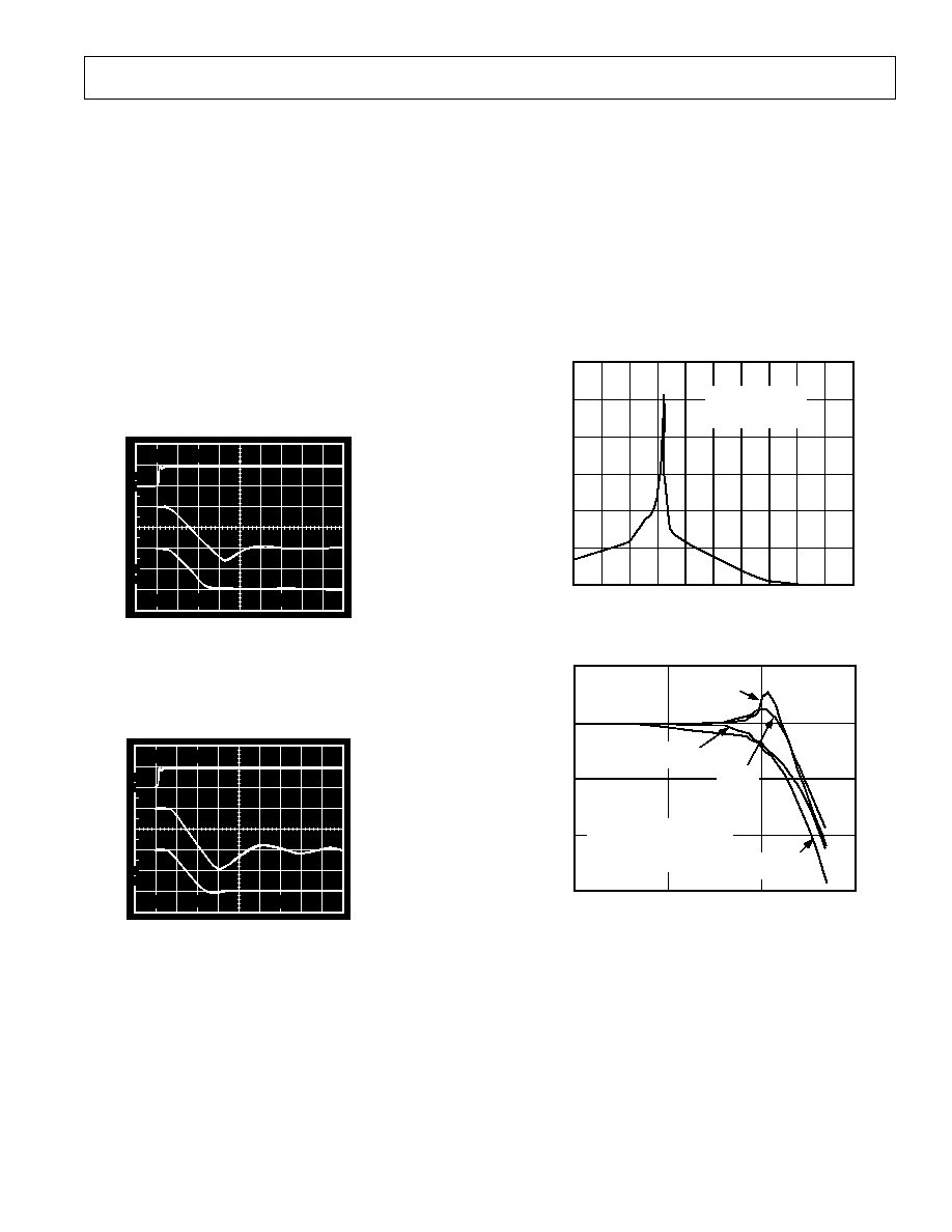
duced by the output capacitance of the D/A converter. Figures
4 and 5 show the performance of the AD7112 using the
AD712, a high speed, low cost BiFET amplifier, and the
OP275, a dual bipolar/JFET amplifier suitable for audio appli-
cations. The performance with and without the compensation
capacitor is shown in both cases. For operation beyond
250 kHz, capacitor C1 may be reduced in value. This gives an
increase in bandwidth at the expense of a poorer transient re-
sponse as shown in Figure 7. In circuits where C1 is not in-
cluded, the high frequency roll-off point is primarily determined
by the characteristics of the output amplifier and not the AD7112.
Feedthrough and accuracy are sensitive to output leakage cur-
rents effects. For this reason it is recommended that the operat-
ing temperature of the AD7112 be kept as close to +25
°
C as is
practically possible, particularly where the devices performance
at high attenuation levels is important. A typical plot of leakage
current vs. temperature is shown in Figure 11.
Some solder fluxes and cleaning materials can form slightly
conductive films which cause leakage effects between analog in-
put and output. The user is cautioned to ensure that the manu-
facturing process for circuits using the AD7112 does not allow
such films to form. Otherwise the feedthrough, accuracy and
maximum usable range will be affected.
STATIC ACCURACY PERFORMANCE
The D/A converter section of the AD7112 consists of a 17-bit
R2R type converter. To obtain optimum static performance at
this level of resolution it is necessary to pay great attention to
amplifier selection, circuit grounding, etc.
Amplifier input bias current results in a dc offset at the output
of the amplifier due to current flowing in the feedback resistor
R
FB
. It is recommended that amplifiers with input bias currents
of less than 10 nA be used (e.g., AD712) to minimize this offset.
AD7112
REV. 0
7
Another error arises from the output amplifier's input offset volt-
age. The amplifier is operated with a fixed feedback resistance,
but the equivalent source impedance (the AD7112 output im-
pedance) varies as a function of the attenuation level. This has
the effect of varying the noise gain of the amplifier thus creating
a varying error due to amplifier offset voltage. It is recom-
mended that an amplifier with less than 50
µ
V of input offset be
used (such as the AD712 or ADOP07) in dc applications. Am-
plifiers with a large input offset voltage may cause audible
thumps in audio applications due to dc output changes. The
AD7112 accuracy is specified and tested using only the internal
feedback resistor. Any gain error (i.e., mismatch of R
FB
to the
R2R ladder) that may exist in the AD7112 D/A converter cir-
cuit results in a constant attenuation error over the whole range.
The AD7112 accuracy is specified relative to 0 dB attenuation,
hence gain trim resistors can be used to adjust V
OUT
= V
IN
pre-
cisely (i.e., 0 dB attenuation) with input code 00000000. For
further information on gain error refer to the "CMOS DAC Ap-
plication Guide" which is available from Analog Devices, Publi-
cation Number G872b-8-1/89.
TYPICAL PERFORMANCE CHARACTERISTICS
I
DD
mA
6
0
5
3
1
2
0
5
4
3
4
2
1
V
IN
Volts
T
A
= +25
°
C
ALL DIGITAL INPUTS
TIED TOGETHER
Figure 6. Supply Current vs. Logic Input Level
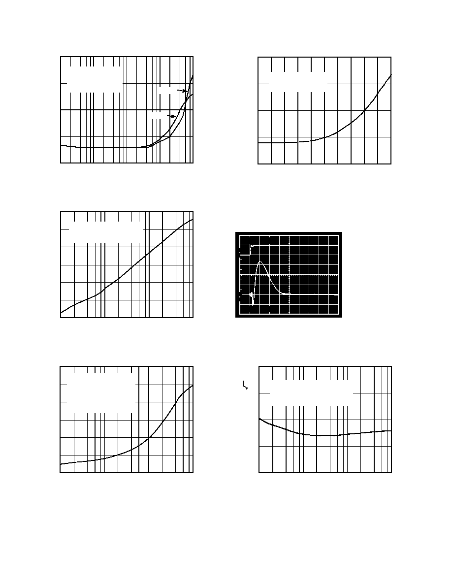
FREQUENCY Hz
NORMALIZED GAIN WITH RESPECT TO 1kHz
OP275
C1 = 0pF
10
30
10
4
10
7
0
20
10
5
10
OP275
C1 = 15pF
AD712
C1 = 0pF
AD712
C1 = 15pF
10
6
V
DD
= +5V
T
A
= +25
°
C
DATA INPUT CODE = 0000 0000
V
IN
= 1V rms
Figure 7. Frequency Response with AD712 and OP275
10
90
100
0%
200ns
5V
C1 = 0pF
C1 = 15pF
DATA CHANGE
FROM 00H TO 80H
5V
A1 0.8V
Figure 4. Response of AD7112 with AD712
10
90
100
0%
200ns
5V
C1 = 0pF
C1 = 15pF
DATA CHANGE
FROM 00H TO 80H
5V
A1 0.8V
Figure 5. Response of AD7112 with OP275
AD7112
REV. 0
8
60
80
100
90
70
10
10
10
10
10
1
2
3
4
5
FREQUENCY Hz
TOTAL HARMONIC DISTORTION dB
OP275
AD712
V
IN
= 6V rms
INPUT CODE = 0000 0000
T = +25
°
C
C1 = 15pF
Figure 8. Distortion vs. Frequency
40
70
100
10
3
10
4
10
6
10
5
80
90
60
50
FREQUENCY Hz
FEEDTHROUGH dB
V
DD
= +5V
T = +25
°
C
V
IN
A, V
IN
B = 20V pp SINE WAVE
Figure 9. Feedthrough vs. Frequency
40
70
100
10
3
10
4
10
6
10
5
80
90
60
50
V
DD
= +5V
T
A
= +25
°
C
V
IN
A = 20V pp SINE WAVE
V
IN
B = 0V
BOTH DAC LATCHES LOADED
WITH 0000 0000
FREQUENCY Hz
CHANNEL-CHANNEL ISOLATION dB
Figure 10. Channel-to-Channel Isolation vs. Frequency
2
0
40
85
15
1
35
60
10
TEMPERATURE
°
C
OUTPUT LEAKAGE CURRENT I
OUT
nA
V
DD
= +5V
V
IN
= 10V
DATA INPUT = 1111 XXXX
Figure 11. Output Leakage Current vs. Temperature
AD712
OUTPUT
DATA INPUTS
FROM 00H TO 80H
10
90
100
0%
200ns
5V
10mV
A1 2.0V
V
DD
= +5V
T
A
= +25
°
C
V
IN
= AGND
Figure 12. Digital-to-Analog Glitch Impulse
FREQUENCY Hz
50
30
10
10
2
10
3
10
5
10
4
V
DD
= +5V
V
IN
= 0V
DAC CODE = 0000 0000
INCLUDES OP275 AMPLIFIER NOISE
20
40
NOISE SPECTRAL DENSITY nV/ Hz
Figure 13. Noise Spectral Density vs. Frequency
AD7112
REV. 0
9
*
0.4
0.6
30
0.0
0.4
3
0.2
0
0.2
27
24
21
18
15
12
9
6
ATTENUATION dB
ERROR dB
**
* * *
* *
*
**
* * *
* *
*
*
*
* * *
* *
*
*
* *
* * * * **
*
*
* *
* *
*
V
DD
= +5V
T
A
= +25
°
C
Figure 14. Typical Attenuation Error for 0.75 dB Steps
1.0
1.0
0
78
0.5
0.5
6
0.0
66
72
60
48
42
36
30
24
18
12
54
84
ATTENUATION dB
ERROR dB
T
A
= +25
°
C
T
A
= +85
°
C
V
DD
= +5V
Figure 15. Typical Attenuation Error for 3 dB Steps vs.
Temperature
1
2
0
90
2
1
6
0
78 84
72
66
60
54
18
12
48
42
36
30
24
ATTENUATION dB
ERROR dB
+0.17
0.17
85.5
0.375 dB ATTENUATION STEPS
MONOTONICITY FOR 1.5 dB ATTENUATION STEPS
0.75 dB ATTENUATION STEPS
Figure 16. Accuracy Specification for B Grade Devices at
T
A
= +25
°
C
1
2
0
90
2
1
6
0
78 84
72
66
60
54
18
12
48
42
36
30
24
ATTENUATION dB
ERROR dB
+0.17
0.17
0.375 dB ATTENUATION STEPS
0.75 dB ATTENUATION STEPS
MONOTONICITY FOR 1.5 dB ATTENUATION STEPS
Figure 17. Accuracy Specification for C Grade Devices at
T
A
= +25
°
C
AD7112
REV. 0
10
MICROPROCESSOR INTERFACING
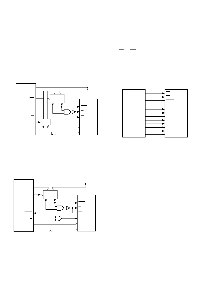
Figures 18 to 20 show interfaces between the AD7112 and
three popular 8-bit microprocessor systems, the MC68008,
8085A/8088 and the 8051. In the MC68008 and 8085/8088 in-
terfaces, the AD7112 is memory mapped with separate ad-
dresses for each DAC.
AD7112-8085A/8088 INTERFACE
Figure 18 shows a connection diagram for interfacing the
AD7112 to both the 8085A and the 8088 microprocessors. This
scheme is also suited to the Z80 microprocessor, but the Z80
address/data bus does not have to be demultiplexed. The
AD7112 is memory mapped with separate memory addresses
for DAC A and DAC B.
8085A / 8088
AD7112*
CS
WR
DB7 DB0
DATA BUS
A15 A8
AD7 AD0
ALE
ADDRESS BUS
WR
DEN
DAC A / DAC B
A**
A+1**
ADDRESS
DECODE
LOGIC
8-BIT
LATCH
*
ANALOG CIRCUITRY HAS BEEN OMITTED FOR CLARITY.
** A = DECODED ADDRESS FOR AD7112 DAC A
A+1 = DECODED ADDRESS FOR AD7112 DAC B
Figure 18. AD71128085A/8088 Interface Circuit
AD711268008 INTERFACE
Figure 19 shows a connection diagram for interfacing the
AD7112 to the 68008 microprocessor. The AD7112 is again
memory mapped with separate memory addresses for DAC A
and DAC B.
AD7112*
CS
WR
DB7 DB0
DATA BUS
ADDRESS BUS
DAC A / DAC B
A**
A+1**
ADDRESS
DECODE
LOGIC
*
ANALOG CIRCUITRY HAS BEEN OMITTED FOR CLARITY.
** A = DECODED ADDRESS FOR AD7112 DAC A
A+1 = DECODED ADDRESS FOR AD7112 DAC B
68008
A23 A1
D7 D0
R /W
AS
DTACK
Figure 19. AD711268008 Interface Circuit
AD71128051 INTERFACE
Figure 20 shows a connection diagram between the AD7112
and the 8051 microprocessor. The AD7112 is port mapped in
this interface. The loading structure is as follows: Data to be
loaded to the DAC is output to Port 1: P3.0, P3.1 and P3.2 are
bit addressable port lines and are used to control the DAC
select, CS and WR inputs. A sample routine for writing to DAC A
is shown below.
MOV A,DATA;
Data to be written is loaded to the accumulator.
CLR 3.2;
Select DAC A.
CLR 3.0;
Bring CS low.
CLR 3.1;
Bring WR low.
MOV A,P1;
Write data to DAC.
SET B 3.1;
Deactivate WR.
SET B 3.0;
Deactivate CS
8051
P3.0
P3.1
P3.2
P1.0
P1.1
P1.2
P1.3
P1.4
P1.5
P1.6
P1.7
AD7112*
CS
WR
DAC A / DAC B
DB0
DB1
DB2
DB3
DB4
DB5
DB6
DB7
* ANALOG CIRCUITRY OMITTED FOR CLARITY
Figure 20. AD71128051 Interface Circuit
APPLICATIONS
Automatic Gain Control
In an automatic gain control system an input signal is attenuated
or amplified so that its average output level remains constant.
The AD7112 D/A converter is used here as a variable gain or at-
tenuation element that adjusts the output signal relative to the
input level.
A feedback loop consisting of a detector, comparator, and up/
down counter continuously adjusts the contents of the counter
and hence the gain or attenuation of the circuit so that the signal
level at the output remains constant and equal to the reference
input signal. The negative feedback action of the loop ensures
that the average output voltage of the automatic gain control
system remains constant. Figure 21 shows a block diagram of a
typical AGC control loop using 1/2 AD7112 as the gain/ attenu-
ation element.
Whenever the input signal is outside the dynamic range of the
programmable gain element in the AGC loop, there should be a
stable, well defined input output relationship.
AD7112
REV. 0
11
OUTPUT
INPUT
VARIABLE
GAIN ELEMENT
1/2 AD7112
D
UP/DOWN COUNTER
U
V
REF
END STOP AND
CONTROL LOGIC
DETECTOR
COMPARATOR
Figure 21. Automatic Gain Control System
Programmable State Variable Filter
The AD7112 with its multiplying capability and fast settling
time is ideal for many types of signal conditioning applications.
The circuit of Figure 22 shows its use in a state variable filter
design. This type of filter has three outputs: low pass, bandpass
and high pass. The particular version shown in Figure 22 uses
two AD7112 to control the critical parameters f
0
, Q and A
0
. In-
stead of several fixed resistors, the circuit uses the DAC equiva-
lent resistances as circuit elements. Thus, R1 in Figure 22 is
controlled by the 8-bit word loaded to DAC A1 of the AD7112.
This is also the case with R2, R3 and R4.
DAC Equivalent Resistance,
R
EQ
=
R
DAC
10
×
EXP (0.375
×
N / 20)
where:
R
DAC
is the DAC ladder resistance.
N is the DAC code in Decimal (0
N
240).
DACs A1 and B1 control the gain and Q of the filter character-
istic while DACs A2 and B2 control the cutoff frequency.
Circuit equations:
C1 = C2, R3 = R4, R7 = R8.
Resonant frequency, f
0
= 1/(2
R3C1).
Quality factor, Q = (R6/R8)
×
(R2/R
FBB1
).
R
FBB1
is the feedback resistance of DAC B1 in Figure 22
Bandpass Gain, A
0
= R2/R1.
Programmable range for component values shown is f
0
= 0 kHz
to 15 kHz and Q = 0.3 to 4.5.
DATA 2
OUT A
AD7112
DAC A1
(R1)
V
IN
A
R
FB
B
C3
10pF
V
IN
NOTES
1. A1, A2, A3, A4 : 1/4 x AD713
2. C3 IS A COMPENSATION CAPACITOR TO ELIMINATE Q AND GAIN VARIATIONS
CAUSED BY AMPLIFIER GAIN BANDWIDTH LIMITATIONS
HIGH
PASS
OUTPUT
OUT B
DAC B1
(R2)
BANDPASS
OUTPUT
V
IN
B
LOW-PASS
OUTPUT
R7
30k
R8
30k
R6
10k
C1
1000pF
C2
1000pF
R5
DB0DB7
CS
WR
DAC A/
DAC B
DATA 1
DAC A2
(R3)
DAC B2
(R4)
A1
OUT A
AD7112
V
IN
A
OUT B
V
IN
B
DB0DB7
CS
WR
DAC A/
DAC B
A2
A3
A4
Figure 22. Programmable State Variable Filter
AD7112
REV. 0
12
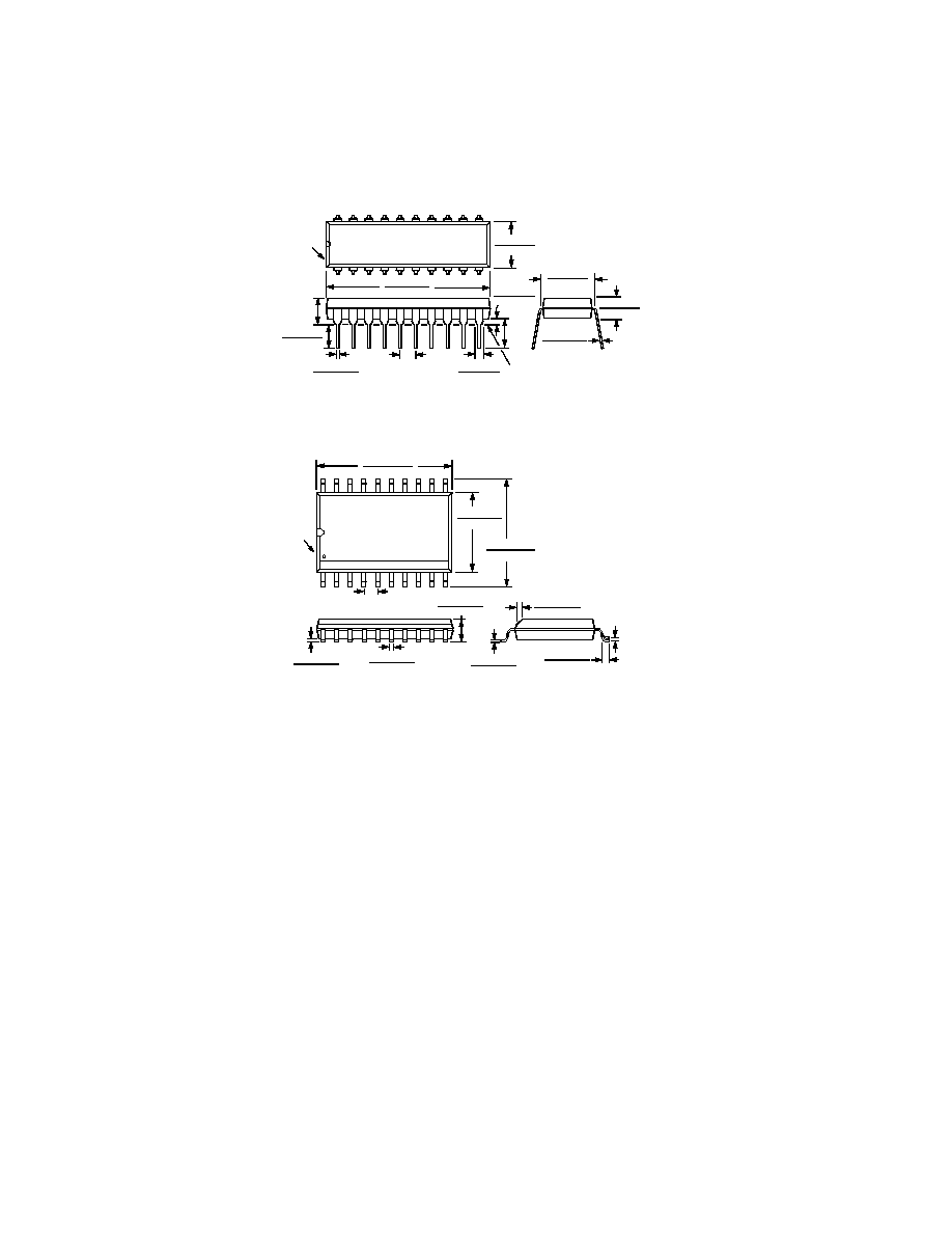
OUTLINE DIMENSIONS
Dimensions shown in inches and (mm).
20-Pin Plastic DIP (N-20)
0.280 (7.11)
0.240 (6.10)
1.060 (26.90)
0.925 (23.50)
0.022 (0.558)
0.014 (0.356)
0.100 (2.54)
BSC
0.160 (4.06)
0.115 (2.93)
0.060 (1.52)
0.015 (0.38)
0.130
(3.30)
MIN
0.070 (1.77)
0.045 (1.15)
0.015 (0.381)
0.008 (0.204)
0.195 (4.95)
0.115 (2.93)
0.325 (8.25)
0.300 (7.62)
PIN 1
10
1
11
20
0.210
(5.33)
MAX
SEATING
PLANE
20-Pin SOIC (R-20)
0.0500 (1.27)
BSC
0.0192 (0.49)
0.0138 (0.35)
0.0118 (0.30)
0.0040 (0.10)
0.0500 (1.27)
0.0157 (0.40)
0.1043 (2.65)
0.0926 (2.35)
0.0125 (0.32)
0.0091 (0.23)
0.4193 (10.65)
0.3937 (10.00)
0.2992 (7.60)
0.2914 (7.40)
0.5118 (13.00)
0.4961 (12.60)
1
10
20
11
PIN 1
0
°-
8
°
0.0291 (0.74)
0.0098 (0.25)
X
45
°
C1692107/92
PRINTED IN U.S.A.