AD7142 Programmable Capacitance-to-Digital Converter with Environmental Compensation Data Sheet (Rev. 0)
Programmable Capacitance-to-Digital
Converter with Environmental
Compensation
AD7142
Rev. 0
Information furnished by Analog Devices is believed to be accurate and reliable. However, no
responsibility is assumed by Analog Devices for its use, nor for any infringements of patents or other
rights of third parties that may result from its use. Specifications subject to change without notice. No
license is granted by implication or otherwise under any patent or patent rights of Analog Devices.
Trademarks and registered trademarks are the property of their respective owners.
One Technology Way, P.O. Box 9106, Norwood, MA 02062-9106, U.S.A.
Tel: 781.329.4700
www.analog.com
Fax: 781.461.3113
©2006 Analog Devices, Inc. All rights reserved.
FEATURES
Programmable capacitance-to-digital converter
36 ms update rate (@ maximum sequence length)
Better than 1 fF resolution
14 capacitance sensor input channels
No external RC tuning components required
Automatic conversion sequencer
On-chip automatic calibration logic
Automatic compensation for environmental changes
Automatic adaptive threshold and sensitivity levels
On-chip RAM to store calibration data
SPI®-compatible serial interface (AD7142)
I
2
C®-compatible serial interface (AD7142-1)
Separate V
DRIVE
level for serial interface
Interrupt output and GPIO
32-lead, 5 mm x 5 mm LFCSP_VQ
2.6 V to 3.6 V supply voltage
Low operating current
Full power mode: less than 1 mA
Low power mode: 50 A
APPLICATIONS
Personal music and multimedia players
Cell phones
Digital still cameras
Smart hand-held devices
Television, A/V, and remote controls
Gaming consoles
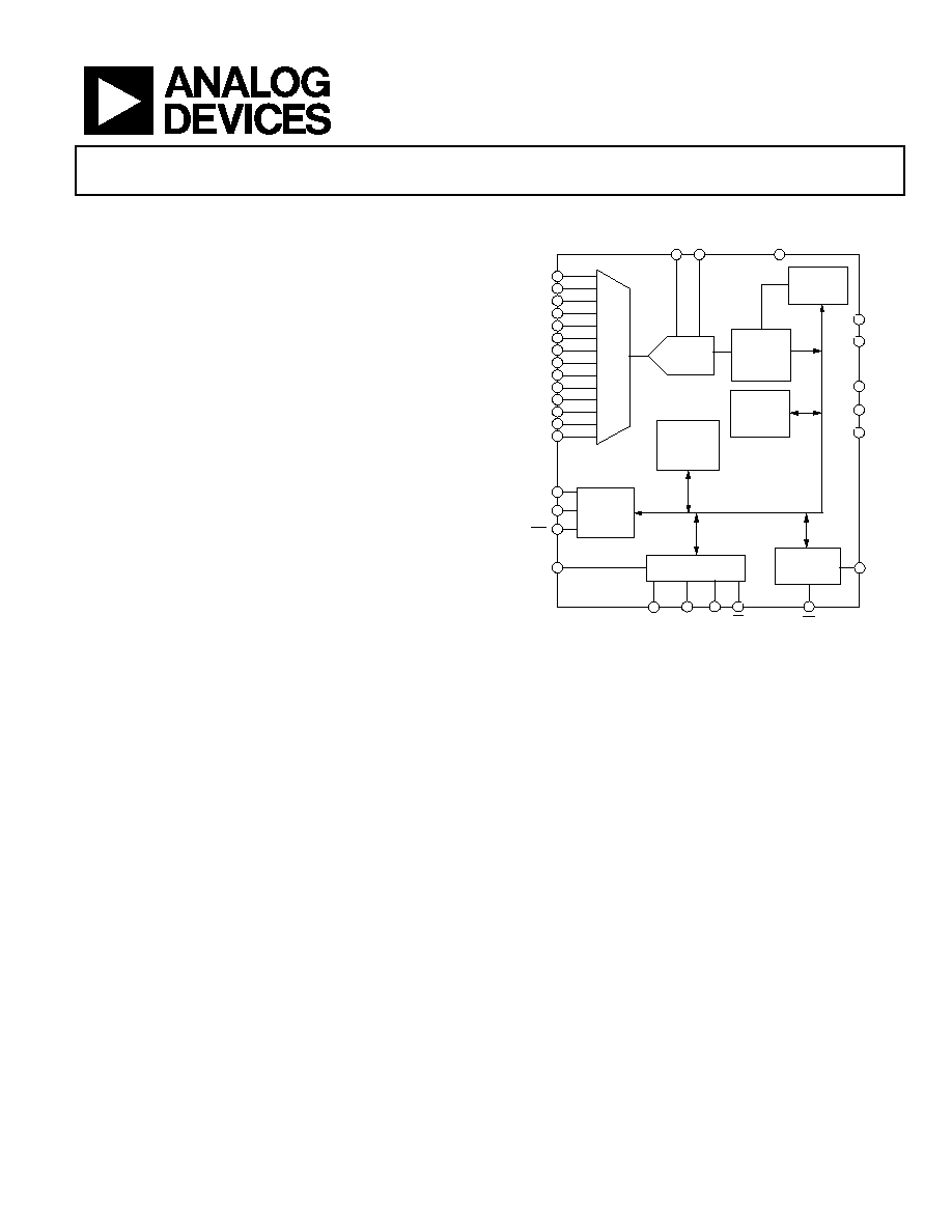
FUNCTIONAL BLOCK DIAGRAM
TEST
V
REF+
V
REF
SDO/
SDA
SDI/
ADD0
SCLK
CS/
ADD1
INT
C
SHIELD
SRC
SRC
V
DRIVE
SW
I
T
C
H
MA
T
R
I
X
16-BIT
-
CDC
CALIBRATION
ENGINE
CONTROL
AND
DATA
REGISTERS
CALIBRATION
RAM
250kHz
EXCITATION
SOURCE
SERIAL INTERFACE
AND CONTROL LOGIC
INTERRUPT
AND GPIO
LOGIC
POWER-ON
RESET
LOGIC
AV
CC
AGND
DGND1
DGND2
DV
CC
GPIO
19
18
17
14
13
27
28
29
CIN0
30
CIN1
31
CIN2
32
CIN3
1
CIN4
2
CIN5
3
CIN6
4
CIN7
5
CIN8
6
CIN9
7
CIN10
8
CIN11
9
CIN12
10
CIN13
11
12
15
16
20
21
22
23
24
25
26
05702-
001
Figure 1.
GENERAL DESCRIPTION
The AD7142 and AD7142-1 are integrated capacitance-to-
digital converters (CDCs) with on-chip environmental
calibration for use in systems requiring a novel user input
method. The AD7142 and AD7142-1 can interface to external
capacitance sensors implementing functions such as capacitive
buttons, scroll bars, or wheels.
The CDC has 14 inputs channeled through a switch matrix to a
16-bit, 250 kHz sigma-delta (-) capacitance-to-digital
converter. The CDC is capable of sensing changes in the
capacitance of the external sensors and uses this information to
register a sensor activation. The external sensors can be
arranged as a series of buttons, as a scroll bar or wheel, or as a
combination of sensor types. By programming the registers, the
user has full control over the CDC setup. High resolution
sensors require minor software to run on the host processor.
The AD7142 and AD7142-1 have on-chip calibration logic to
account for
changes in the ambient environment. The calibration
sequence is performed automatically and at continuous intervals,
while the sensors are not touched. This ensures that there are no
false or nonregistering touches on the external sensors due to a
changing environment.
The AD7142 has an SPI-compatible serial interface, and the
AD7142-1 has an I
2
C-compatible serial interface. Both parts
have an interrupt output, as well as a general-purpose input/
output (GPIO).
The AD7142 and AD7142-1 are available in a 32-lead, 5 mm ×
5 mm LFCSP_VQ and operate from a 2.6 V to 3.6 V supply. The
operating current consumption is less than 1 mA, falling to
50 A in low power mode (conversion interval of 400 ms).

AD7142
Rev. 0 | Page 2 of 68
TABLE OF CONTENTS
Features .............................................................................................. 1
Applications....................................................................................... 1
Functional Block Diagram .............................................................. 1
General Description ......................................................................... 1
Revision History ............................................................................... 2
Specifications..................................................................................... 3
SPI Timing Specifications (AD7142)......................................... 5
I
2
C Timing Specifications (AD7142-1) ..................................... 6
Absolute Maximum Ratings............................................................ 7
ESD Caution.................................................................................. 7
Pin Configurations and Function Descriptions ........................... 8
Typical Performance Characteristics ............................................. 9
Theory of Operation ...................................................................... 11
Capacitance Sensing Theory..................................................... 11
Operating Modes........................................................................ 12
Capacitance Sensor Input Configuration.................................... 13
CIN Input Multiplexer Setup .................................................... 13
Capacitiance-to-Digital Converter............................................... 14
Oversampling the CDC Output ............................................... 14
Capacitance Sensor Offset Control.......................................... 14
Conversion Sequencer ............................................................... 14
CDC Conversion Sequence Time ............................................ 15
CDC Conversion Results........................................................... 16
Noncontact Proximity Detection ................................................. 17
Recalibration ............................................................................... 17
Proximity Sensitivity .................................................................. 17
FIFO Control .............................................................................. 20
Environmental Calibration ........................................................... 22
Capacitance Sensor Behavior Without Calibration............... 22
Capacitance Sensor Behavior with Calibration...................... 23
Adaptive Threshold and Sensitivity ............................................. 24
Interrupt Output............................................................................. 25
CDC Conversion Complete Interrupt..................................... 25
Sensor Touch Interrupt.............................................................. 25
GPIO INT Output Control ....................................................... 27
Outputs ............................................................................................ 29
Excitation Source........................................................................ 29
C
SHIELD
Output ............................................................................. 29
GPIO ............................................................................................ 29
Using the GPIO to turn on/off an LED................................... 29
Serial Interface ................................................................................ 30
SPI Interface ................................................................................ 30
I
2
C Compatible Interface........................................................... 32
V
DRIVE
Input ................................................................................. 34
PCB Design Guidelines ................................................................. 35
Capacitive Sensor Board Mechanical Specifications ............. 35
Chip Scale Packages ................................................................... 35
Power-Up Sequence ....................................................................... 36
Typical Application Circuits ......................................................... 37
Register Map ................................................................................... 38
Detailed Register Descriptions ..................................................... 39
Bank 1 Registers ......................................................................... 39
Bank 2 Registers ......................................................................... 48
Bank 3 Registers ......................................................................... 54
Outline Dimensions ....................................................................... 66
Ordering Guide .......................................................................... 66
REVISION HISTORY
6/06--Revision 0: Initial Version

AD7142
Rev. 0 | Page 3 of 68
SPECIFICATIONS
AV
CC
, DV
CC
= 2.6 V to 3.6 V, T
A
= -40
o
C to +85°C, unless otherwise noted.
Table 1.
Parameter Min
Typ
Max
Unit
Test
Conditions/Comments
CAPACITANCE-TO-DIGITAL CONVERTER
Update Rate
35.45
36.86
38.4
ms
12 conversion stages in sequencer,
decimation = 256
Resolution
16
Bit
CIN Input Range
1
±2
pF
No Missing Codes
16
Bit
Guaranteed by design, but not production
tested
CIN Input Leakage
25
nA
Total Unadjusted Error
±20
%
Output Noise (Peak-to-Peak)
7
Codes
Decimation rate = 128
3
Codes
Decimation rate = 256
Output Noise (RMS)
0.8
Codes
Decimation rate = 128
0.5
Codes
Decimation rate = 256
Parasitic Capacitance
40
pF
Parasitic capacitance to ground, per CIN input
guaranteed by characterization
C
BULK
Offset Range
1
±20
pF
C
BULK
Offset Resolution
156.25
fF
Low Power Mode Delay Accuracy
4
%
% of 200 ms, 400 ms, 600 ms, or 800 ms
EXCITATION SOURCE
Frequency 240
250
260
kHz
Output Voltage
AV
CC
V
Short-Circuit Source Current
20
mA
Short-Circuit Sink Current
50
mA
Maximum Output Load
250
pF
Capacitance load on source to ground
C
SHIELD
Output Drive
10
A
C
SHIELD
Bias Level
AV
CC
/2
V
LOGIC INPUTS (SDI, SCLK, CS, SDA, GPI TEST)
V
IH
Input High Voltage
0.7 x V
DRIVE
V
V
IL
Input Low Voltage
0.4
V
I
IH
Input High Voltage
-1
A
V
IN
= V
DRIVE
I
IL
Input Low Voltage
1
A
V
IN
= DGND
Hysteresis
150
mV
OPEN-DRAIN OUTPUTS (SCLK, SDA, INT)
V
OL
Output Low Voltage
0.4
V
I
SINK
= -1 mA
I
OH
Output High Leakage Current
+0.1
±1
A
V
OUT
= V
DRIVE
LOGIC OUTPUTS (SDO, GPO)
V
OL
Output Low Voltage
0.4
V
I
SINK
= 1 mA, V
DRIVE
= 1.65 V to 3.6 V
V
OH
Output High Voltage
V
DRIVE
- 0.6
V
I
SOURCE
= 1 mA, V
DRIVE
= 1.65 V to 3.6 V
SDO Floating State Leakage Current
±1
A
Pin three-state, leakage measured to GND and
DV
CC
GPO Floating State Leakage Current
-5
+2
A
Pin three-state, leakage measured to GND and
DV
CC
AD7142
Rev. 0 | Page 4 of 68
Parameter Min
Typ
Max
Unit
Test
Conditions/Comments
POWER
AV
CC
, DV
CC
2.6 3.3
3.6 V
V
DRIVE
1.65
3.6
V
Serial interface operating voltage
I
CC
0.9
1
mA
In full power mode
20
A
Low power mode, converter idle, T
A
= 25°C
16
33
A
Low power mode, converter idle
4.5
A
Full
shutdown,
T
A
= 25°C
2.25
18
A
Full
shutdown
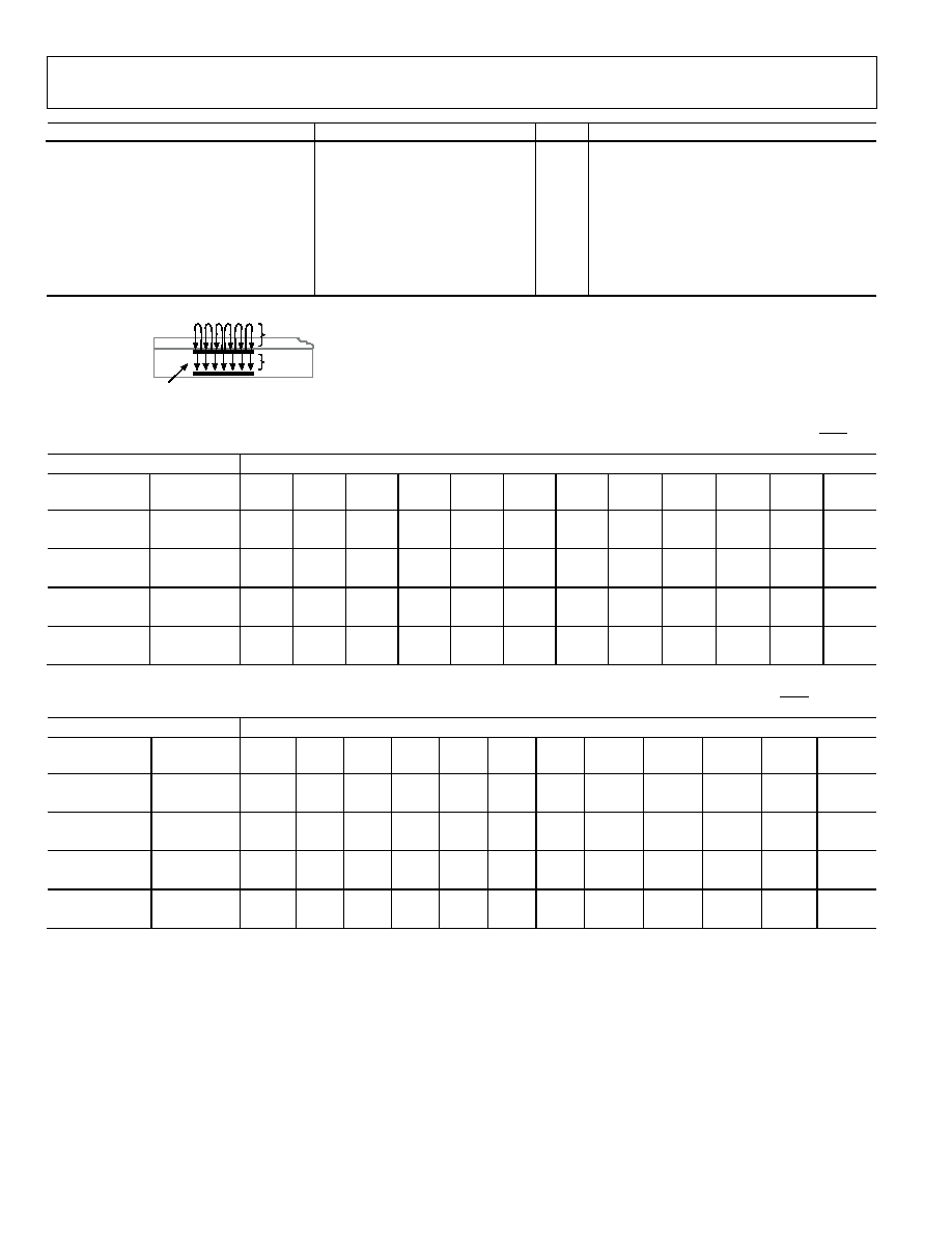
PLASTIC OVERLAY
1
C
IN
and C
BULK
are defined as follows:
SENSOR BOARD
C
BULK
C
IN
CAPACITIVE SENSOR
05
70
2-
05
4
Table 2. Typical Average Current in Low Power Mode, AV
CC
, DV
CC
= 3.6 V, T= 25°C, Load of 50 pF on SRC Pin, No Load on SRC
Number of Conversion Stages, Current Values Expressed in A
Low Power
Mode Delay
Decimation
Rate =
1
2
3
4
5
6
7
8
9
10
11
12
200 ms
128
26.4
33.3
40.1
46.9
53.5
60
66.5
72.8
79.1
85.2
91.3
97.3
256
35.6
49.1
62.2
74.9
87.3
99.3
111
122.3
133.4
144.2
154.7
164.9
400 ms
128
21.3
24.8
28.3
31.7
35.2
38.6
42
45.4
48.7
52
55.3
58.6
256
26
32.9
39.7
46.5
53.1
59.6
66.1
72.4
78.7
84.9
91
97
600 ms
128
19.6
21.9
24.3
26.6
28.9
31.2
33.5
35.8
38.1
40.4
42.6
44.8
256
22.7
27.4
32
36.6
41.1
45.6
50
54.4
58.8
63.1
67.4
71.6
800 ms
128
18.7
20.5
22.2
24
25.7
27.5
29.2
31
32.7
34.4
36.1
37.8
256
21.1
24.6
28.1
31.5
35
38.4
41.8
45.2
48.5
51.8
55.1
58.4
Table 3. Maximum Average Current in Low Power Mode, AV
CC
, DV
CC
= 3.6 V, Load of 50 pF on SRC Pin, No Load on SRC
Number of Conversion Stages, Current Values Expressed in A
Low Power
Mode Delay
Decimation
Rate =
1
2
3
4
5
6
7
8
9
10
11
12
200 ms
128
45.4
53.6
61.5
69.4
77.1
84.7
92.2
99.6
106.8
113.9
121
127.9
256
56.2
72
87.2
102
116.3
130.2
143.7
156.8
169.5
181.8
193.8
205.5
400 ms
128
39.5
43.6
47.7
51.8
55.8
59.8
63.7
67.6
71.5
75.4
79.2
83
256
45
53.1
61.1
68.9
76.7
84.3
91.8
99.1
106.4
113.6
120.6
127.5
600 ms
128
37.5
40.3
43
45.8
48.5
51.2
53.9
56.5
59.2
61.8
64.5
67.1
256
41.2
46.7
52.1
57.4
62.7
67.9
73.1
78.2
83.3
88.3
93.3
98.2
800 ms
128
36.5
38.6
40.7
42.7
44.8
46.8
48.8
50.9
52.9
54.9
56.9
58.9
256
39.3
43.4
47.5
51.5
55.6
59.5
63.5
67.4
71.3
75.2
79
82.8
AD7142
Rev. 0 | Page 5 of 68
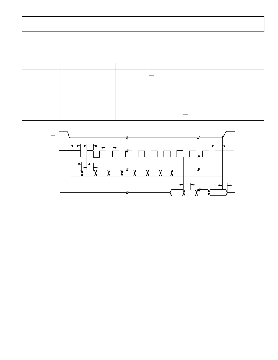
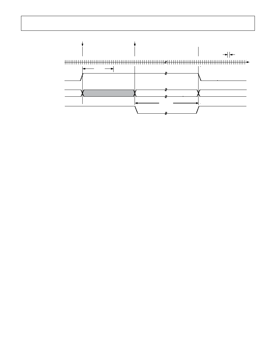
SPI TIMING SPECIFICATIONS (AD7142)
T
A
= -40°C to +85°C; V
DRIVE
= 1.65 V to 3.6 V; AV
CC
, DV
CC
= 2.6 V to 3.6 V, unless otherwise noted. Sample tested at 25°C to ensure
compliance. All input signals are specified with t
R
= t
F
= 5 ns (10% to 90% of V
CC
) and timed from a voltage level of 1.6 V.
Table 4. SPI Timing Specifications
Parameter
Limit at T
MIN
, T
MAX
Unit Description
f
SCLK
5
MHz max
t
1
5
ns min
CS falling edge to first SCLK falling edge
t
2
20
ns min
SCLK high pulse width
t
3
20
ns min
SCLK low pulse width
t
4
15
ns min
SDI setup time
t
5
15
ns min
SDI hold time
t
6
20
ns max
SDO access time after SCLK falling edge
t
7
16
ns max
CS rising edge to SDO high impedance
t
8
15 ns
min
SCLK rising edge to CS high
CS
SCLK
SDI
SDO
t
1
1
16
15
MSB
LSB
2
3
MSB
LSB
1
2
15
16
t
2
t
4
t
5
t
3
t
6
t
7
t
8
05
70
2-
0
02
Figure 2. SPI Detailed Timing Diagram
AD7142
Rev. 0 | Page 6 of 68
I
2
C TIMING SPECIFICATIONS (AD7142-1)
T
A
= -40°C to +85°C; V
DRIVE
= 1.65 V to 3.6 V; AV
CC
, DV
CC
= 2.6 V to 3.6 V, unless otherwise noted. Sample tested at 25°C to ensure
compliance. All input signals timed from a voltage level of 1.6 V.
Table 5. I
2
C Timing Specifications
1
Parameter
Limit
Unit
Description
f
SCLK
400
kHz max
t
1
0.6
s min
Start condition hold time, t
HD; STA
t
2
1.3
s min
Clock low period, t
LOW
t
3
0.6
s min
Clock high period, t
HIGH
t
4
100
ns min
Data setup time, t
SU; DAT
t
5
300
ns min
Data hold time, t
HD; DAT
t
6
0.6
s min
Stop condition setup time, t
SU; STO
t
7
0.6
s min
Start condition setup time, t
SU; STA
t
8
1.3
s min
Bus free time between stop and start conditions, t
BUF
t
R
300
ns max
Clock/data rise time
t
F
300
ns max
Clock/data fall time
1
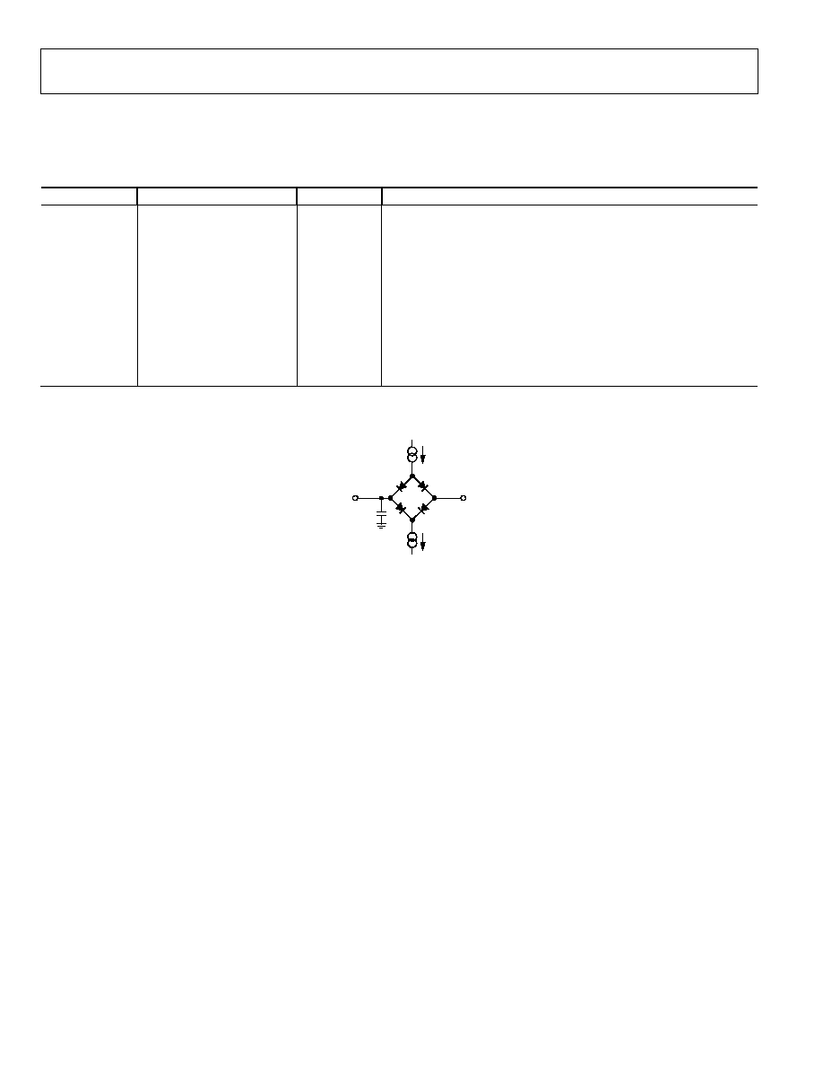
Guaranteed by design, not production tested.
200µA
I
OL
200µA
I
OH
1.6V
TO OUTPUT
PIN
C
L
50pF
05
70
2
-
00
4
Figure 3. Load Circuit for Digital Output Timing Specifications
AD7142
Rev. 0 | Page 7 of 68
ABSOLUTE MAXIMUM RATINGS
Table 6.
Parameter Rating
AV
CC
to AGND, DV
CC
to DGND
-0.3 V to +3.6 V
Analog Input Voltage to AGND
-0.3 V to AV
CC
+ 0.3 V
Digital Input Voltage to DGND
-0.3 V to V
DRIVE
+ 0.3 V
Digital Output Voltage to DGND
-0.3 V to V
DRIVE
+ 0.3 V
Input Current to Any Pin Except
Supplies
1
10 mA
ESD Rating (Human Body Model)
2.5 kV
Operating Temperature Range
-40°C to +150°C
Storage Temperature Range
-65°C to +150°C
Junction Temperature
150°C
LFCSP_VQ
Power Dissipation
450 mW
JA
Thermal Impedance
135.7°C/W
IR Reflow Peak Temperature
260°C (±0.5°C)
Lead Temperature (Soldering 10 sec)
300°C
1
Transient currents of up to 100 mA do not cause SCR latch-up.
Stresses above those listed under Absolute Maximum Ratings
may cause permanent damage to the device. This is a stress
rating only; functional operation of the device at these or any
other conditions above those indicated in the operational
section of this specification is not implied. Exposure to absolute
maximum rating conditions for extended periods may affect
device reliability.
ESD CAUTION
ESD (electrostatic discharge) sensitive device. Electrostatic charges as high as 4000 V readily accumulate on
the human body and test equipment and can discharge without detection. Although this product features
proprietary ESD protection circuitry, permanent damage may occur on devices subjected to high energy
electrostatic discharges. Therefore, proper ESD precautions are recommended to avoid performance
degradation or loss of functionality.
AD7142
Rev. 0 | Page 8 of 68
PIN CONFIGURATIONS AND FUNCTION DESCRIPTIONS
0
57
02
-
00
5
PIN 1
INDICATOR
1
CIN3
2
CIN4
3
CIN5
4
CIN6
5
CIN7
6
CIN8
7
CIN9
8
CIN10
24 CS
23 SCLK
22 SDI
21 SDO
20 V
DRIVE
19 DGND2
18 DGND1
17 DV
CC
9
C
I
N
1
1
1
0
C
I
N
1
2
1
1
C
I
N
1
3
1
2
C
S
H
I
E
L
D
1
3
A
V
C
C
1
4
A
G
N
D
1
5
S
R
C
1
6
S
R
C
3
2
C
I
N
2
3
1
C
I
N
1
3
0
C
I
N
0
2
9
V
R
E
F
2
8
V
R
E
F
+
2
7
T
E
S
T
2
6
G
P
I
O
2
5
I
N
T
TOP VIEW
AD7142
Figure 4. AD7142 Pin Configuration
PIN 1
INDICATOR
1
CIN3
2
CIN4
3
CIN5
4
CIN6
5
CIN7
6
CIN8
7
CIN9
8
CIN10
24 ADD1
23 SCLK
22 ADD0
21 SDA
20 V
DRIVE
19 DGND2
18 DGND1
17 DV
CC
9
C
I
N
1
1
1
0
C
I
N
1
2
1
1
C
I
N
1
3
1
2
C
S
H
I
E
L
D
1
3
A
V
C
C
1
4
A
G
N
D
1
5
S
R
C
1
6
S
R
C
3
2
C
I
N
2
3
1
C
I
N
1
3
0
C
I
N
0
2
9
V
R
E
F
2
8
V
R
E
F
+
2
7
T
E
S
T
2
6
G
P
I
O
2
5
I
N
T
TOP VIEW
AD7142-1
05
702
-
04
4
Figure 5. AD7142-1 Pin Configuration
Table 7. Pin Function Descriptions
Pin No.
Mnemonic
Description
1
CIN3
Capacitance Sensor Input.
2
CIN4
Capacitance Sensor Input.
3
CIN5
Capacitance Sensor Input.
4
CIN6
Capacitance Sensor Input.
5
CIN7
Capacitance Sensor Input.
6
CIN8
Capacitance Sensor Input.
7
CIN9
Capacitance Sensor Input.
8
CIN10
Capacitance Sensor Input.
9
CIN11
Capacitance Sensor Input.
10
CIN12
Capacitance Sensor Input.
11
CIN13
Capacitance Sensor Input.
12 C
SHIELD
CDC Shield Potential Output. Requires 10 nF capacitor to ground. Connect to external shield.
13 AV
CC
CDC Supply Voltage.
14
AGND
Analog Ground Reference Point for All CDC Circuitry. Tie to analog ground plane.
15
SRC
CDC Excitation Source Output.
16
SRC
Inverted Excitation Source Output.
17 DV
CC
Digital Core Supply Voltage.
18 DGND1
Digital
Ground.
19 DGND2
Digital
Ground.
20 V
DRIVE
Serial Interface Operating Voltage Supply.
21
SDO
AD7142 SPI Serial Data Output.
SDA AD7142-1
I
2
C Serial Data Input/Output. SDA requires pull-up resistor.
22
SDI
AD7142 SPI Serial Data Input.
ADD0
AD7142-1
I
2
C Address Bit 0.
23
SCLK
Clock Input for Serial Interface.
24
CS
AD7142 SPI Chip Select Signal.
ADD1
AD7142-1
I
2
C Address Bit 1.
25
INT
General-Purpose Open-Drain Interrupt Output. Programmable polarity; requires pull-up resistor.
26 GPIO Programmable
GPIO.
27
TEST
Factory Test Pin. Tie to ground.
28 V
REF+
CDC Positive Reference Input. Normally tied to analog power.
29 V
REF-
CDC Negative Reference Input. Tie to analog ground.
30
CIN0
Capacitance Sensor Input.
31
CIN1
Capacitance Sensor Input.
32
CIN2
Capacitance Sensor Input.
AD7142
Rev. 0 | Page 9 of 68
TYPICAL PERFORMANCE CHARACTERISTICS
05
70
2-
0
53
I
CC
(µ
A
)
V
CC
(V)
820
860
840
920
900
880
940
960
980
1000
2.7
2.9
2.8
3.0
3.1
3.2
3.3
3.4
3.5
3.6
DEVICE 3
DEVICE 1
DEVICE 2
Figure 6. Supply Current vs. Supply Voltage
(V
CC
= AV
CC
+ DV
CC
, I
CC
= AI
CC
+ DI
CC
)
2.7
2.8
2.9
3.0
3.1
3.2
3.4
3.3
3.5
3.6
0
570
2-
0
51
I
CC
(µ
A
)
V
CC
(V)
40
60
100
80
120
140
160
180
LP_CONV_DELAY = 200ms
LP_CONV_DELAY = 400ms
LP_CONV_DELAY = 600ms
LP_CONV_DELAY = 800ms
Figure 7. Low Power Supply Current vs. Supply Voltage,
Decimation Rate = 256 (V
CC
= AV
CC
+ DV
CC
, I
CC
= AI
CC
+ DI
CC
)
2.7
2.8
2.9
3.0
3.10
3.2
3.4
3.3
3.5
3.6
05
70
2-
0
50
I
CC
(µ
A
)
V
CC
(V)
20
40
60
80
100
120
LP_CONV_DELAY = 200ms
LP_CONV_DELAY = 600ms
LP_CONV_DELAY = 800ms
LP_CONV_DELAY = 400ms
Figure 8. Low Power Supply Current vs. Supply Voltage
Decimation Rate = 128 (V
CC
= AV
CC
+ DV
CC
, I
CC
= AI
CC
+ DI
CC
)
1.40
1.55
1.70
1.85
2.00
2.15
2.30
2.45
2.7
2.9
2.8
3.0
3.1
3.2
3.3
3.4
3.5
3.6
S
HUT
DO
W
N I
CC
(µA
)
V
CC
(V)
05
70
2-
0
52
DEVICE 2
DEVICE 3
DEVICE 1
Figure 9. Shutdown Supply Current vs. Supply Voltage
(V
CC
= AV
CC
+ DV
CC
, I
CC
= AI
CC
+ DI
CC
)
1.10
1.05
1.00
0.95
0.90
0.85
0.80
0
50
100
150
200
250
300
350
400
450
500
05
70
2-
04
9
I
CC
(m
A
)
CAPACITANCE LOAD ON SOURCE (pF)
DEVICE 3
DEVICE 2
DEVICE 1
Figure 10. Supply Current vs. Capacitive Load on SRC (I
CC
= AI
CC
+ DI
CC
)
16015
16010
16005
16000
15995
15990
15985
15980
0
50
100
150
200
250
300
350
400
450
500
05
702
-
04
8
CDC O
UT
P
UT
CO
DE
CAPACITANCE LOAD ON SOURCE (pF)
DEVICE 3
DEVICE 2
DEVICE 1
Figure 11. Output Code vs. Capacitive Load on SRC
AD7142
Rev. 0 | Page 10 of 68
960
780
800
820
840
860
880
900
920
940
40
120
100
3.6V
3.3V
2.7V
80
60
40
20
0
20
05
70
2-
0
56
S
UP
P
L
Y
CURRE
NT
(
µ
A
)
TEMPERATURE (°C)
Figure 12. Supply Current vs. Temperature (Supply Current = AI
CC
+ DI
CC
)
12
10
8
6
4
2
0
40
120
100
80
60
40
2.7V
3.3V
20
0
20
05
70
2-
0
57
S
UP
P
L
Y
CURRE
NT
(
µ
A
)
TEMPERATURE (°C)
3.6V
Figure 13. Shutdown Supply Current vs. Temperature
(Supply Current = AI
CC
+ DI
CC
)
2.5
2.0
1.5
1.0
0.5
0
10
10M
100k
1k
05
70
2-
0
59
C
D
C
PEA
K
-
T
O
-
PEA
K
N
O
I
S
E (C
o
d
e
s
)
FREQUENCY (Hz)
100mV
200mV
300mV
400mV
500mV
Figure 14. Power Supply Sine Wave Rejection
180
160
140
120
100
80
60
40
20
0
100
10M
25mV
100mV
200mV
300mV
1M
10k
100k
1k
05
70
2-
0
60
C
D
C
PEA
K
-
T
O
-
PEA
K
N
O
I
S
E (C
o
d
e
s
)
SQUARE WAVE FREQUENCY (Hz)
50mV
Figure 15. Power Supply Square Wave Rejection
AD7142
Rev. 0 | Page 11 of 68
THEORY OF OPERATION
The AD7142 and AD7142-1 are capacitance-to-digital
converters (CDCs) with on-chip environmental compensation,
intended for use in portable systems requiring high resolution
user input. The internal circuitry consists of a 16-bit, - con-
verter that converts a capacitive input signal into a digital value.
There are 14 input pins on the AD7142 and AD7142-1, CIN0 to
CIN13. A switch matrix routes the input signals to the CDC.
The result of each capacitance-to-digital conversion is stored in
on-chip registers. The host subsequently reads the results over
the serial interface. The AD7142 contains an SPI interface and
the AD7142-1 has an I
2
C interface ensuring that the parts are
compatible with a wide range of host processors. Because the
AD7142 and AD7142-1 are identical parts, with the exception of
the serial interface, AD7142 refers to both the AD7142 and
AD7142-1 throughout this data sheet.
The AD7142 interfaces with up to 14 external capacitance
sensors. These sensors can be arranged as buttons, scroll bars,
wheels, or as a combination of sensor types. The external
sensors consist of electrodes on a 2- or 4-layer PCB that
interfaces directly to the AD7142.
The AD7142 can be set up to implement any set of input
sensors by programming the on-chip registers. The registers can
also be programmed to control features such as averaging,
offsets, and gains for each of the external sensors. There is a
sequencer on-chip to control how each of the capacitance
inputs is polled.
The AD7142 has on-chip digital logic and 528 words of RAM
that are used for environmental compensation. The effects of
humidity, temperature, and other environmental factors can
effect the operation of capacitance sensors. Transparent to the
user, the AD7142 performs continuous calibration to compen-
sate for these effects, allowing the AD7142 to give error-free
results at all times.
The AD7142 requires some minor companion software that
runs on the host or other microcontroller to implement high
resolution sensor functions such as a scroll bar or wheel.
However, no companion software is required to implement
buttons, including 8-way button functionality. Button sensors
are implemented completely in digital logic on-chip.
The AD7142 can be programmed to operate in either full power
mode, or in low power automatic wake-up mode. The
automatic wake-up mode is particularly suited for portable
devices that require low power operation giving the user
significant power savings coupled with full functionality.
The AD7142 has an interrupt output, INT, to indicate when
new data has been placed into the registers. INT is used to
interrupt the host on sensor activation. The AD7142 operates
from a 2.6 V to 3.6 V supply, and is available in a 32-lead, 5 mm ×
5 mm LFCSP_VQ.
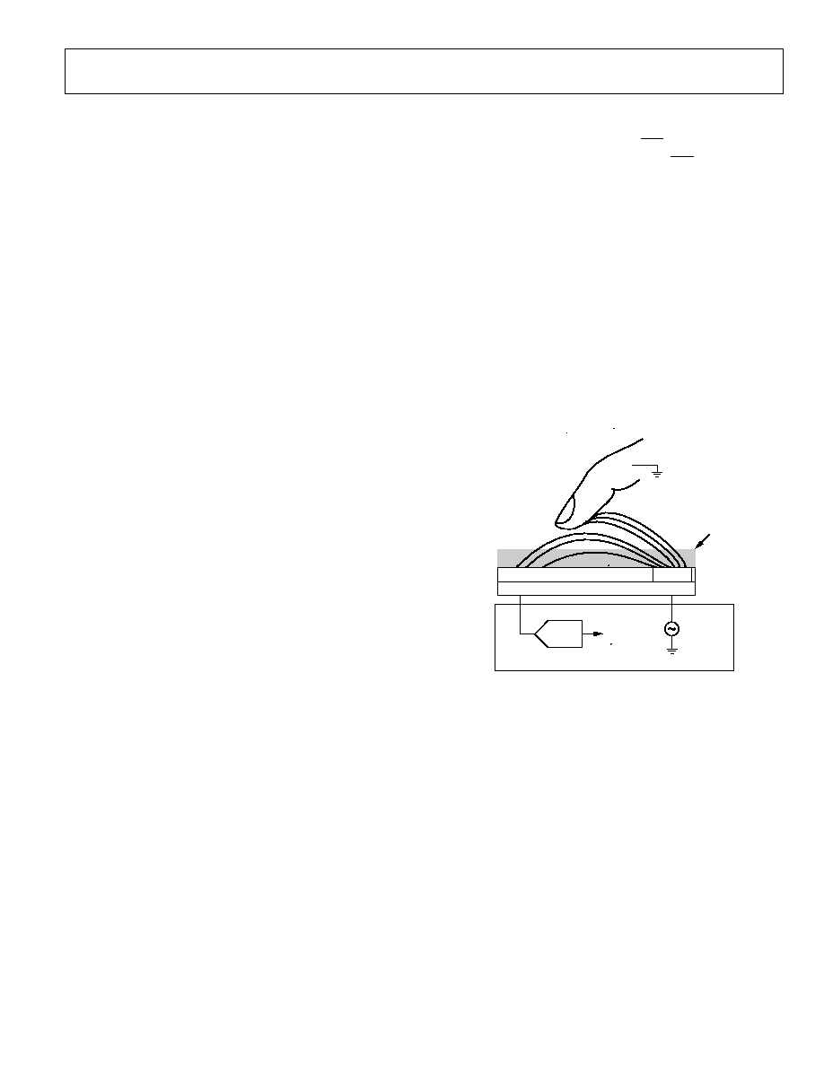
CAPACITANCE SENSING THEORY
The AD7142 uses a method of sensing capacitance known as
the shunt method. Using this method, an excitation source is
connected to a transmitter generating an electric field to a
receiver. The field lines measured at the receiver are translated
into the digital domain by a - converter. When a finger, or
other grounded object, interferes with the electric field, some of
the field lines are shunted to ground and do not reach the
receiver (see Figure 16). Therefore, the total capacitance
measured at the receiver decreases when an object comes close
to the induced field.
EXCITATION
SIGNAL
240kHz
-
ADC
16-BIT
DATA
05
70
2-
0
07
PLASTIC COVER
AD7142
Tx
Rx
PCB LAYER 1
PCB LAYER 2
Figure 16. Sensing Capacitance Method
In practice, the excitation source and - ADC are implemented
on the AD7142, while the transmitter and receiver are constructed
on a PCB that makes up the external sensor.
Registering a Sensor Activation
When a sensor is approached, the total capacitance associated
with that sensor, measured by the AD7142, changes. When the
capacitance changes to such an extent that a set threshold is
exceeded, the AD7142 registers this as a sensor touch.
Preprogrammed threshold levels are used to determine if a
change in capacitance is due to a button being activated. If the
capacitance exceeds one of the threshold limits, the AD7142
registers this as a true button activation. The same thresholds
principle is used to determine if other types of sensors, such as
sliders or scroll wheels, are activated.
AD7142
Rev. 0 | Page 12 of 68
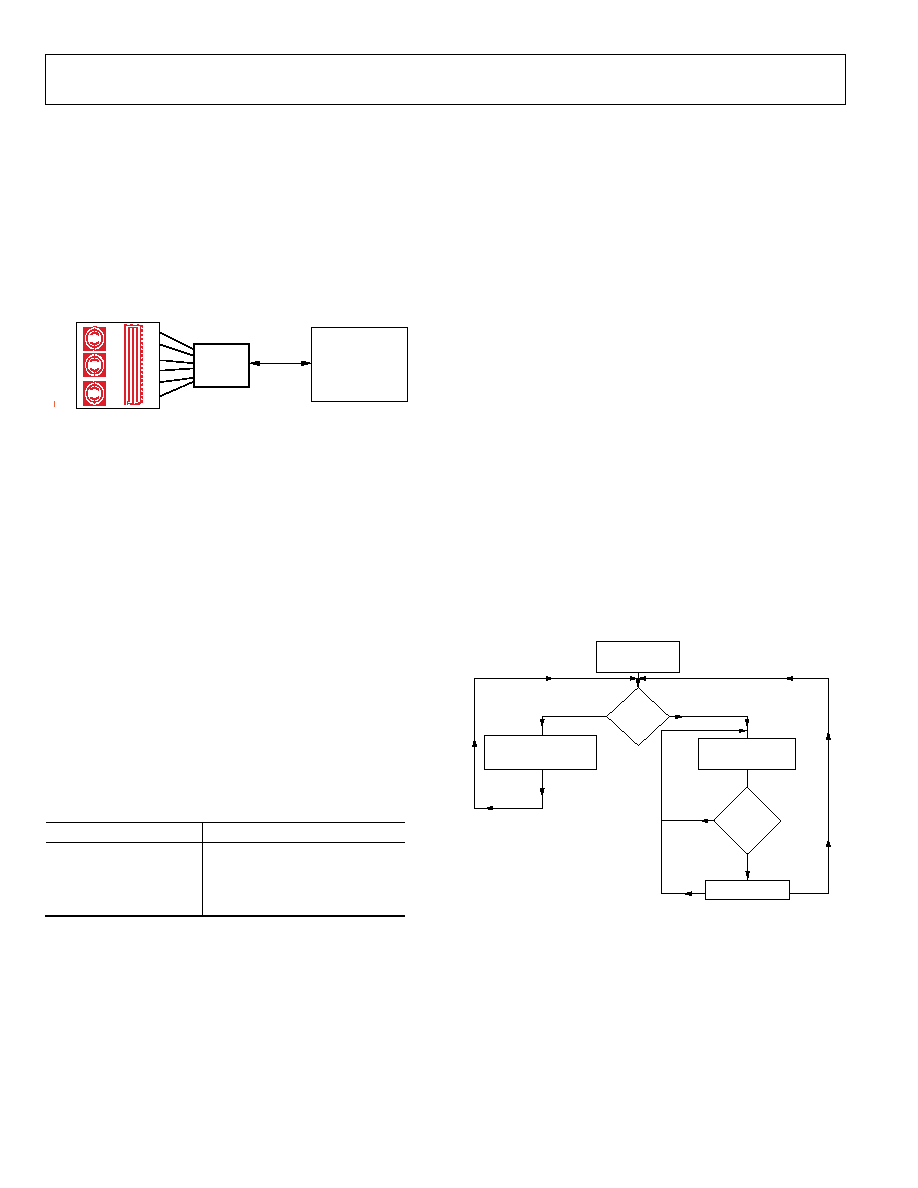
Complete Solution for Capacitance Sensing
Analog Devices provides a complete solution for capacitance
sensing. The two main elements to the solution are the sensor
PCB and the AD7142.
If the application requires high resolution sensors such as scroll
bars or wheels, software is required that runs on the host
processor. (No software is required for button sensors.) The
memory requirements for the host depend on the sensor, and
are typically 10 kB of code and 600 bytes of data memory.
0
5702
-
0
08
HOST PROCESSOR
1 MIPS
10kB ROM
600 BYTES RAM
AD7142
SPI OR I
2
C
SENSOR PCB
Figure 17. Three Part Capacitance Sensing Solution
Analog Devices supplies the sensor PCB design to the customer
based on the customer's specifications, and supplies any necessary
software on an open-source basis. Standard sensor designs are
also available as PCB library components.
OPERATING MODES
The AD7142 has three operating modes. Full power mode,
where the device is always fully powered, is suited for applications
where power is not a concern (for example, game consoles that
have an ac power supply). Low power mode, where the part
automatically powers down, is tailored to give significant power
savings over full power mode, and is suited for mobile applications
where power must be conserved. In shutdown mode, the part
shuts down completely.
The POWER_MODE bits (Bit 0 and Bit 1) of the control
register set the operating mode on the AD7142. The control
register is at Address 0x000. Table 8 shows the POWER_MODE
settings for each operating mode. To put the AD7142 into
shutdown mode, set the POWER_MODE bits to either 01 or 11.
Table 8. POWER_MODE Settings
POWER_MODE Bits
Operating Mode
00
Full power mode
01
Full shutdown mode
10
Low power mode
11
Full shutdown mode
The power-on default setting of the POWER_MODE bits is 00,
full power mode.
Full Power Mode
In full power mode, all sections of the AD7142 remain fully
powered at all times. While a sensor is being touched, the
AD7142 processes the sensor data. If no sensor is touched, the
AD7142 measures the ambient capacitance level and uses this
data for the on-chip compensation routines. In full power
mode, the AD7142 converts at a constant rate. See the CDC
Conversion Sequence Time section for more information.
Low Power Mode
When in low power mode, the AD7142 POWER_MODE bits
are set to 10 upon device initialization. If the external sensors
are not touched, the AD7142 reduces its conversion frequency,
thereby greatly reducing its power consumption. The part
remains in a low power state while the sensors are not touched.
Every 400 ms, the AD7142 performs a conversion and uses this
data to update the compensation logic. When an external
sensor is touched, the AD7142 begins a conversion sequence
every 40 ms to read back data from the sensors. In low power
mode, the total current consumption of the AD7142 is an
average of the current used during a conversion, and the
current used while the AD7142 is waiting for the next
conversion to begin. For example, when the low power mode
conversion interval is 400 ms, the AD7142 typically uses 0.9 mA
current for 40 ms, and 15 A for 400 ms of the conversion
interval. (Note that these conversion timings can be altered
through the register settings. See the CDC Conversion
Sequence Time section for more information.)
NO
YES
YES
NO
TIMEOUT
057
02
-
0
09
ANY SENSOR
TOUCHED?
PROXIMITY TIMER
COUNT DOWN
CONVERSION SEQUENCE
EVERY 36ms FOR
SENSOR READBACK
ANY
SENSOR
TOUCHED?
CONVERSION SEQUENCE
EVERY LP_CONV_DELAY ms
UPDATE COMPENSATION
LOGIC DATA PATH
AD7142 SETUP
AND INITIALIZATION
POWER_MODE = 10
Figure 18. Low Power Mode Operation
AD7142
Rev. 0 | Page 13 of 68
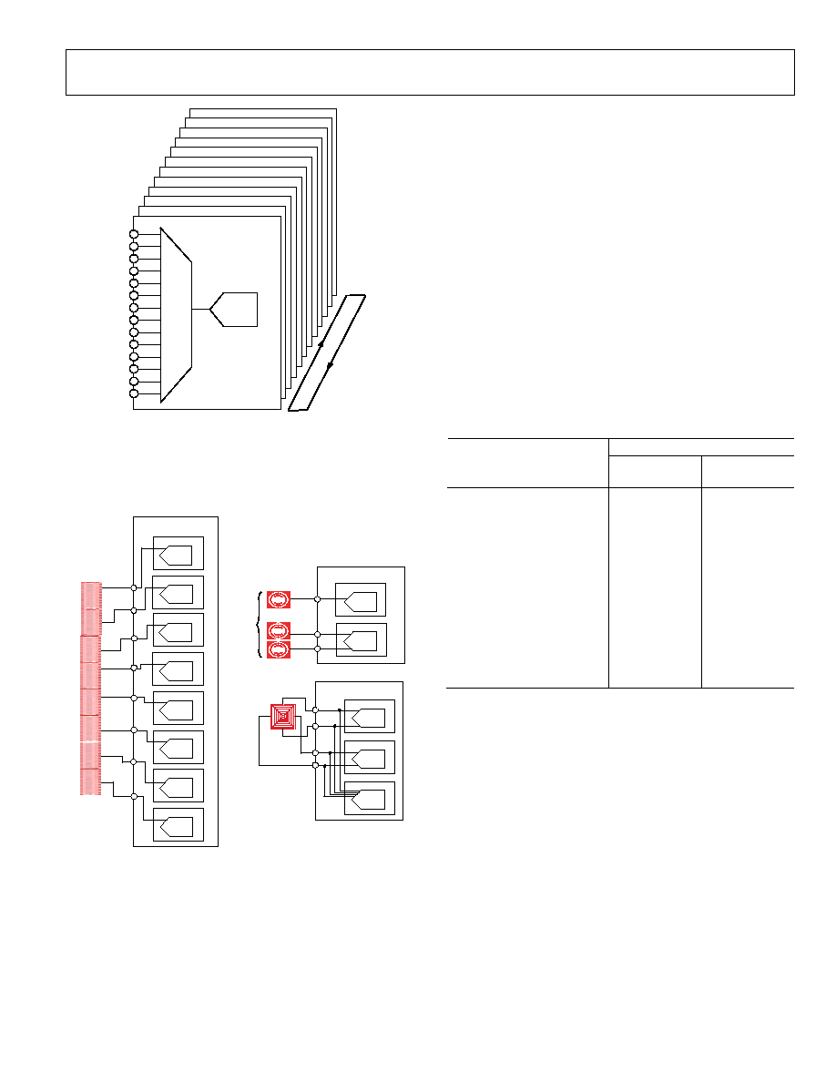
CAPACITANCE SENSOR INPUT CONFIGURATION
Each stage of the AD7142 capacitance sensors can be uniquely
configured by using the registers in Table 45 and Table 46. These
registers are used to configure input pin connection setups,
sensor offsets, sensor sensitivities, and sensor limits for each
stage. Each sensor can be individually optimized. For example,
a button sensor connected to STAGE0 can require a different
sensitivity and offset values than a button with a different
function that is connected to a different stage.
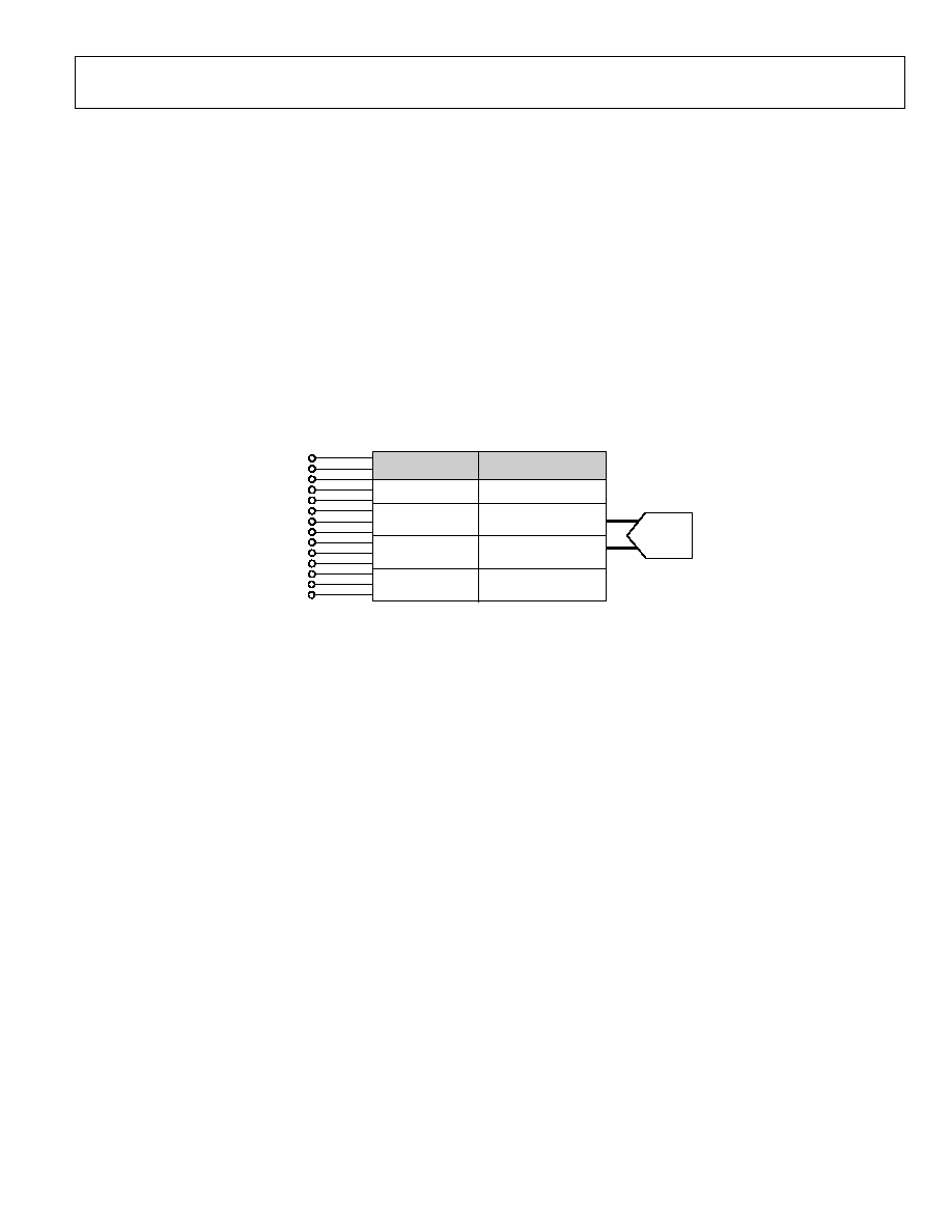
CIN INPUT MULTIPLEXER SETUP
The CIN_CONNECTION_SETUP registers in Table 45 list the
different options that are provided for connecting the sensor
input pin to the CDC converter.
The AD7142 has an on-chip multiplexer to route the input
signals from each pin to the input of the converter. Each input
pin can be tied to either the negative or the positive input of the
CDC, or it can be left floating. Each input can also be internally
connected to the C
SHIELD
signal to help prevent cross coupling. If
an input is not used, always connect it to C
SHIELD.
For each input pin, CIN0 to CIN13, the multiplexer settings can
be set on a per sequencer stage basis. For example, CIN0 is
connected to the negative CDC input for conversion STAGE1,
left floating for sequencer STAGE1, and so on for all twelve
conversion stages.
Two bits in each register control the mux setting for the input pin.
CIN0
CIN1
CIN2
CIN3
CIN4
CIN5
CIN6
CIN7
CIN8
CIN9
CIN10
CIN11
CIN SETTING
CIN_CONNECTION
_SETUP BITS
00
CINX FLOATING
01
CINX CONNECTED TO
NEGATIVE CDC INPUT
10
CINX CONNECTED TO
POSITIVE CDC INPUT
11
CINX CONNECTED TO
C
SHIELD
CDC
+
05702-
0
10
CIN12
CIN13
Figure 19. Input Mux Configuration Options
AD7142
Rev. 0 | Page 14 of 68
CAPACITIANCE-TO-DIGITAL CONVERTER
The capacitance-to-digital converter on the AD7142 has a -
architecture with 16-bit resolution. There are 14 possible inputs
to the CDC that are connected to the input of the converter
through a switch matrix. The sampling frequency of the CDC is
250 kHz.
OVERSAMPLING THE CDC OUTPUT
The decimation rate, or oversampling ratio, is determined by
Bits[9:8] of the control register, as listed in Table 9.
Table 9. CDC Decimation Rate
Decimation Bit Value
Decimation Rate
CDC Output Rate
Per Stage
00 256
1.536
ms
01 128
3.072
ms
10
1
11
1
1
Do not use this setting.
The decimation process on the AD7142 is an averaging process
where a number of samples are taken and the averaged result is
output. Due to the architecture of the digital filter employed, the
amount of samples taken (per stage) is equal to 3× the
decimation rate. So 3 × 256 or 3 × 128 samples are averaged to
obtain each stage result.
The decimation process reduces the amount of noise present in
the final CDC result. However, the higher the decimation rate,
the lower the output rate per stage, thus, a trade-off is possible
between a noise free signal and speed of sampling.
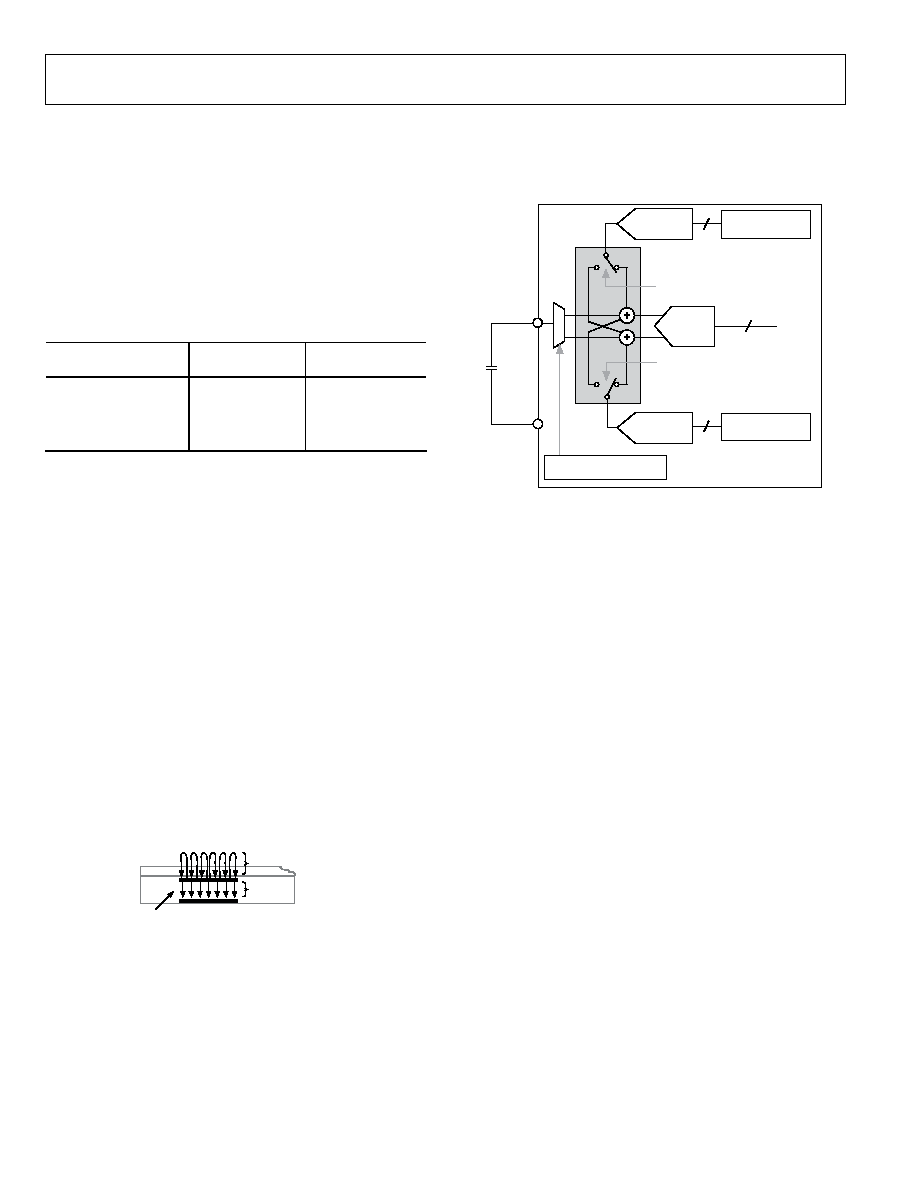
CAPACITANCE SENSOR OFFSET CONTROL
There are two programmable DACs on board the AD7142 to
null any capacitance sensor offsets. These offsets are associated
with printed circuit board capacitance or capacitance due to any
other source, such as connectors. In Figure 20, C
IN
is the
capacitance of the input sensors, while C
BULK
is the capacitance
between layers of the sensor PCB. C
BULK
can be offset using the
on-board DACs.
PLASTIC OVERLAY
SENSOR BOARD
C
BULK
C
IN
CAPACITIVE SENSOR
05
70
2-
05
4
Figure 20. Capacitances Around the Sensor PCB
A simplified block diagram in Figure 21 shows how to apply the
STAGE_OFFSET registers to null the offsets. The 7-bit
POS_AFE_OFFSET and NEG_AFE_OFFSET registers program
the offset DAC to provide 0.16 pF resolution offset adjustment
over a range of ±20 pF. Apply the positive and negative offsets
to either the positive or the negative CDC input using the
NEG_AFE_OFFSET register and POS_AFE_OFFSET register.
This process is only required once during the initial capacitance
sensor characterization.
POS_AFE_OFFSET
REGISTER
16-BIT
CDC
NEG_AFE_OFFSET
REGISTER
+DAC
(20pF RANGE)
POS_AFE_OFFSET_SWAP
REGISTER
NEG_AFE_OFFSET_SWAP
REGISTER
7
7
16
CIN
EXT
CIN_CONNECTION_SETUP
REGISTER
SE
N
S
O
R
DAC
(20pF RANGE)
+
_
05
70
2-
0
1
1
Figure 21. Analog Front End Offset Control
CONVERSION SEQUENCER
The AD7142 has an on-chip sequencer to implement
conversion control for the input channels. Up to 12 conversion
stages can be performed in sequence. By using the Bank 2
registers, each stage can be uniquely configured to support
multiple capacitance sensor interface requirements. For
example, a slider sensor can be assigned to STAGE1 with a
button sensor assigned to STAGE2.
The AD7142 on-chip sequence controller provides conversion
control beginning with STAGE0. Figure 22 shows a block diagram of
the CDC conversion stages and CIN inputs. A conversion sequence is
defined as a sequence of CDC conversions starting at STAGE0 and
ending at the stage determined by the value programmed in the
SEQUENCE_STAGE_NUM register. Depending on the number and
type of capacitance sensors that are used, not all conversion stages are
required. Use the SEQUENCE_STAGE_NUM register to set the
number of conversions in one sequence, depending on the sensor
interface requirements. For example, this register would be set to 5 if
the CIN inputs were mapped to only six stages. In addition, set the
STAGE_CAL_EN registers according to the number of stages that
are used.
AD7142
Rev. 0 | Page 15 of 68
CIN0
CIN1
CIN2
CIN3
CIN4
CIN5
CIN6
CIN7
CIN8
CIN9
CIN10
CIN1 1
CIN12
CIN13
STAGE 0
STAGE 1
STAGE 2
STAGE 3
STAGE 4
STAGE 5
STAGE 6
STAGE 7
STAGE 8
STAGE 9
STAGE 10
STAGE 11
SW
IT
C
H
M
A
T
R
IX
-
16-BIT
ADC
CO
NV
E
RS
IO
N
S
E
Q
U
E
NCE
05
70
2-
01
2
Figure 22. CDC Conversion Stages
The number of required conversion stages depends completely
on the number of sensors attached to the AD7142. Figure 23
shows how many conversion stages are required for each sensor,
and how many inputs each sensor requires to the AD7142.
05
702
-
014
BU
T
T
O
NS
STAGEX
CDC
STAGEX
CDC
+
STAGEX
SCROLL BAR
8-WAY SWITCH
CDC
+
+
STAGEX
+
CDC
STAGEX
+
CDC
STAGEX
+
CDC
AD7142 SEQUENCER
CDC
STAGEX
+
STAGEX
+
CDC
CDC
STAGEX
+
STAGEX
+
CDC
CDC
STAGEX
+
STAGEX
+
CDC
AD7142 SEQUENCER
AD7142 SEQUENCER
STAGEX
+
CDC
Figure 23. Sequencer Setup for Sensors
A button sensor generally requires one sequencer stage;
however, it is possible to configure two button sensors to
operate differentially. Only one button from the pair can be
activated at a time; pressing both buttons together results in
neither button being activated. This configuration requires one
conversion stage.
A scroll bar sensor requires eight stages. The result from each stage
is used by the host software to determine the user's position on the
scroll bar. The algorithm that performs this process is available
from Analog Devices free of charge, on signing a software license.
Scroll wheels also require eight stages.
The 8-way switch is made from two pairs of differential buttons.
It, therefore, requires two conversion stages, one for each of the
differential button pairs. It also requires a stage to measure
whether the sensor is active. The buttons are orientated so that
one pair makes up the top and bottom portions of the 8-way
switch; the other pair makes up the left and right portions of the
8-way switch.
CDC CONVERSION SEQUENCE TIME
The time required for one complete measurement for all 12 stages
by the CDC is defined as the CDC conversion sequence time. The
SEQUENCE_STAGE_NUM register and DECIMATION register
determine the conversion time as listed in Table 10.
Table 10. CDC Conversion Times for Full Power Mode
Conversion Time (ms)
SEQUENCE_STAGE_NUM
DECIMATION
= 128
DECIMATION
= 256
0 1.536
3.072
1 3.072
6.144
2 4.608
9.216
3 6.144
12.288
4 7.68
15.36
5 9.216
18.432
6 10.752
21.504
7 12.288
24.576
8 13.824
27.648
9 15.36
30.72
10 16.896
33.792
11 18.432
36.864
For example, while operating with a decimation rate of 128,
if the SEQUENCE_STAGE_NUM register is set to 5 for the
conversion of six stages in a sequence, the conversion sequence
time is 9.216 ms.
Full Power Mode CDC Conversion Sequence Time
The full power mode CDC conversion sequence time for all 12
stages is set by configuring the SEQUENCE_STAGE_NUM
register, and DECIMATION register as outlined in Table 10.
Figure 24 shows a simplified timing diagram of the full power
CDC conversion time. The full power mode CDC conversion
time t
CONV_FP
is set using Table 10.
AD7142
Rev. 0 | Page 16 of 68
NOTES
1.
t
CONV_FP
= VALUE SET FROM TABLE 10.
t
CONV_FP
CONVERSION
SEQUENCE N
CONVERSION
SEQUENCE N+1
CONVERSION
SEQUENCE N+2
CDC
CONVERSION
05
70
2-
01
5
Figure 24. Full Power Mode CDC Conversion Sequence Time
Low Power Mode CDC Conversion Sequence Time with
Delay
The frequency of each CDC conversion while operating in the
low power automatic wake up mode is controlled by using the
LP_CONV_DELAY register located at Address 0x000[3:2], in
addition to the registers listed in Table 10. This feature provides
some flexibility for optimizing the conversion time to meet
system requirements vs. AD7142 power consumption.
For example, maximum power savings is achieved when the
LP_CONV_DELAY register is set to 3. With a setting of 3, the
AD7142 automatically wakes up, performing a conversion every
800 ms.
Table 11. LP_CONV_DELAY Settings
LP_CONV_DELAY Bits
Delay Between Conversions
00
200 ms
01
400 ms
10
600 ms
11
800 ms
Figure 25 shows a simplified timing example of the low power
CDC conversion time. As shown, the low power CDC
conversion time is set by t
CONV_FP
and the LP_CONV_DELAY
register.
NOTES
1.
t
CONV_LP
= t
CONV_FP
+ LP_CONV_DELAY
t
CONV_LP
CONVERSION
SEQUENCE N
CDC
CONVERSION
05
70
2-
0
1
6
CONVERSION
SEQUENCE N+1
Figure 25. Low Power Mode CDC Conversion Sequence Time
CDC CONVERSION RESULTS
Certain high resolution sensors require the host to read back
the CDC conversion results for processing. The registers
required for host processing are located in the Bank 3 registers.
The host processes the data readback from these registers using
a software algorithm, to determine position information.
In addition to the results registers in the Bank 3 registers, the
AD7142 provides the 16-bit CDC output data directly, starting
at Address 0x00B of Bank 1. Reading back the CDC 16-bit
conversion data register allows for customer-specific application
data processing.
AD7142
Rev. 0 | Page 17 of 68
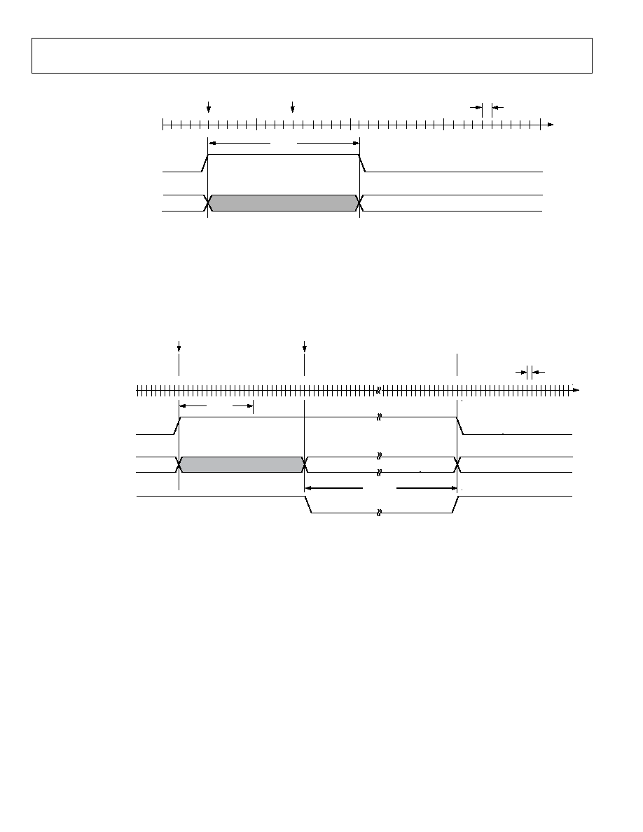
NONCONTACT PROXIMITY DETECTION
The AD7142 internal signal processing continuously monitors
all capacitance sensors for noncontact proximity detection. This
feature provides the ability to detect when a user is approaching
a sensor, at which time all internal calibration is immediately
disabled while the AD7142 is automatically configured to detect
a valid contact.
The proximity control register bits are described in Table 12. The
FP_PROXIMITY_CNT register bits and LP_PROXIMITY_CNT
register bits control the length of the calibration disable period
after proximity is detected. The calibration is disabled during this
time and enabled again at the end of this period provided that the
user is no longer approaching, or in contact with, the sensor.
Figure 26 and Figure 27 show examples of how these registers are
used to set the full and low power mode calibration disable
periods.
RECALIBRATION
In the event of a very long proximity detection event, such as a
user hovering over a sensor for a long period of time, the
FP_PROXIMITY_RECAL Bits[9:0] and LP_PROXIMITY_RECAL
Bits[15:10] in Register 0x004 can be applied to force a recalibration.
This ensures that the ambient values are recalibrated regardless of how
long the user hovers over a sensor. A recalibration ensures maximum
AD7142 sensor performance. Figure 28 and Figure 29 show examples
of using the FP_PROXIMITY_RECAL and
LP_PROXIMITY_RECAL register bits to force a recalibration while
operating in the full and low power modes. These figures show a user
approaching a sensor followed by the user leaving the sensor while the
proximity detection remains active after the user leaves the sensor. This
situation could occur if the user interaction creates some moisture on
the sensor causing the new sensor value to be different from the
expected value. In this case, the internal recalibration is applied to
automatically recalibrate the sensor. The force recalibration event takes
two interrupt cycles, therefore it should not be set again during this
interval.
PROXIMITY SENSITIVITY
Figure 30 describes the two conditions that set the internal
proximity detection signal using Comparator 1 and
Comparator 2. Comparator 1 detects when a user is approach-
ing a sensor. The PROXIMITY_DETECTION_RATE register
controls the sensitivity of Comparator 1. For example, if
PROXIMITY_DETECTION_RATE is set to 4, the Proximity 1
signal is set when the absolute difference between WORD1 and
WORD3 exceeds four LSB codes. Comparator 2 detects when a
user hovers over a sensor or approaches a sensor very slowly.
The PROXIMITY_RECAL_LVL register (Address 0x003)
controls the sensitivity of Comparator 2. For example, if
PROXIMITY_RECAL_LVL is set to 75, the Proximity 2 signal
is set when the absolute difference between the fast filter
average value and the ambient value exceeds 75 LSB codes.
Table 12. Proximity Control Registers (See Figure 30)
Register Length
Register
Address
Description
FP_PROXIMITY_CNT
4 bits
0x002
Full power mode proximity control
LP_PROXIMITY_CNT
4 bits
0x002
Low power mode proximity control
FP_PROXIMITY_RECAL
8 bits
0x004
Full power mode proximity recalibration control
LP_PROXIMITY_RECAL
6 bits
0x004
Low power mode proximity recalibration control
PROXIMITY_RECAL_LVL
8 bits
0x003
Proximity recalibration level
PROXIMITY_DETECTION_RATE
6 bits
0x003
Proximity detection rate
CALIBRATION ENABLED
CALIBRATION DISABLED
PROXIMITY DETECTION
(INTERNAL)
CALIBRATION
(INTERNAL)
t
CALDIS
t
CONV_FP
1 2 3 4 5 6 7 8 9 10 11 1213 14 15 16
CDC CONVERSION SEQUENCE
(INTERNAL)
05
70
2-
0
17
USER LEAVES SENSOR
AREA HERE
USER APPROACHES
SENSOR HERE
Figure 26. Full Power Mode Proximity Detection Example with FP_PROXIMITY = 1
AD7142
Rev. 0 | Page 18 of 68
NOTES
1. SEQUENCE CONVERSION TIME
t
CONV_LP
=
t
CONV_FP
+ LP_CONV_DELAY
2. PROXIMITY IS SET WHEN USER APPROACHES THE SENSOR AT WHICH TIME THE INTERNAL CALIBRATION IS DISABLED.
3.
t
CALDIS
= (
t
CONV_LP
× LP_PROXIMITY_CNT × 4) + LP_CONV_DELAY
CALIBRATION ENABLED
CALIBRATION DISABLED
PROXIMITY DETECTION
(INTERNAL)
CALIBRATION
(INTERNAL)
t
CALDIS
t
CONV_LP
1 2 3 4 5 6 7 8 9 10 11 1213 14 15 16
CDC CONVERSION SEQUENCE
(INTERNAL)
05
70
2-
01
8
USER LEAVES SENSOR
AREA HERE
USER APPROACHES
SENSOR HERE
Figure 27. Low Power Mode Proximity Detection with LP_PROXIMITY = 4 and LP_CONV_DELAY = 0
CALIBRATION ENABLED
CALIBRATION DISABLED
t
DISCA L
t
RECAL
16
30
70
t
CONV_FP
USER IN CONTACT WITH SENSOR
CDC CONVERSION VALUES EXCEED
PROXIMITY_RECALIBRATION _LVL
RECALIBRATION PERIOD
PROXIMITY DETECTION
(INTERNAL)
CALIBRATION
(INTERNAL)
CDC CONVERSION SEQUENCE
(INTERNAL)
RECALIBRATION
(INTERNAL)
0
57
02-
01
9
NOTES
1. SEQUENCE CONVERSION TIME
t
CONV_FP
DETERMINED FROM TABLE 10
2.
t
DISCAL
=
t
CONV_FP
× FP_PROXIMITY_CNT
3.
t
RECAL
=
t
CONV_FP
× FP_PROXIMITY_RECAL
USER APPROACHES
SENSOR HERE
USER LEAVES SENSOR
AREA HERE
Figure 28. Full Power Mode Proximity Detection with Forced Recalibration Example with FP_PROXIMITY = 1 and FP_PROXIMITY_RECAL = 40
AD7142
Rev. 0 | Page 19 of 68
NOTES
1. SEQUENCE CONVERSION TIME
t
CONV_LP
=
t
CONV_HP
+ LP_CONV_DELAY
2.
t
DISCAL
=
t
CONV_LP
× (16 × LP_PROXIMITY_CNT)
3.
t
RECAL
=
t
CONV_LP
× (LP_PROXIMITY_RECAL × 4)
CALIBRATION ENABLED
CALIBRATION DISABLED
t
DISCAL
t
RECAL
16
30
70
t
CONV_LP
RECALIBRATION PERIOD
PROXIMITY DETECTION
(INTERNAL)
CALIBRATION
(INTERNAL)
CDC CONVERSION SEQUENCE
(INTERNAL)
RECALIBRATION
(INTERNAL)
057
02
-
0
20
USER IN CONTACT WITH SENSOR
CDC CONVERSION VALUES EXCEED
PROXIMITY_RECALIBRATION _LVL
USER APPROACHES
SENSOR HERE
USER LEAVES SENSOR
AREA HERE
Figure 29. Low Power Mode Proximity Detection with Forced Recalibration Example with LP_PROXIMITY = 4 and LP_PROXIMITY_RECAL = 10

AD7142
Rev. 0 | Page 20 of 68
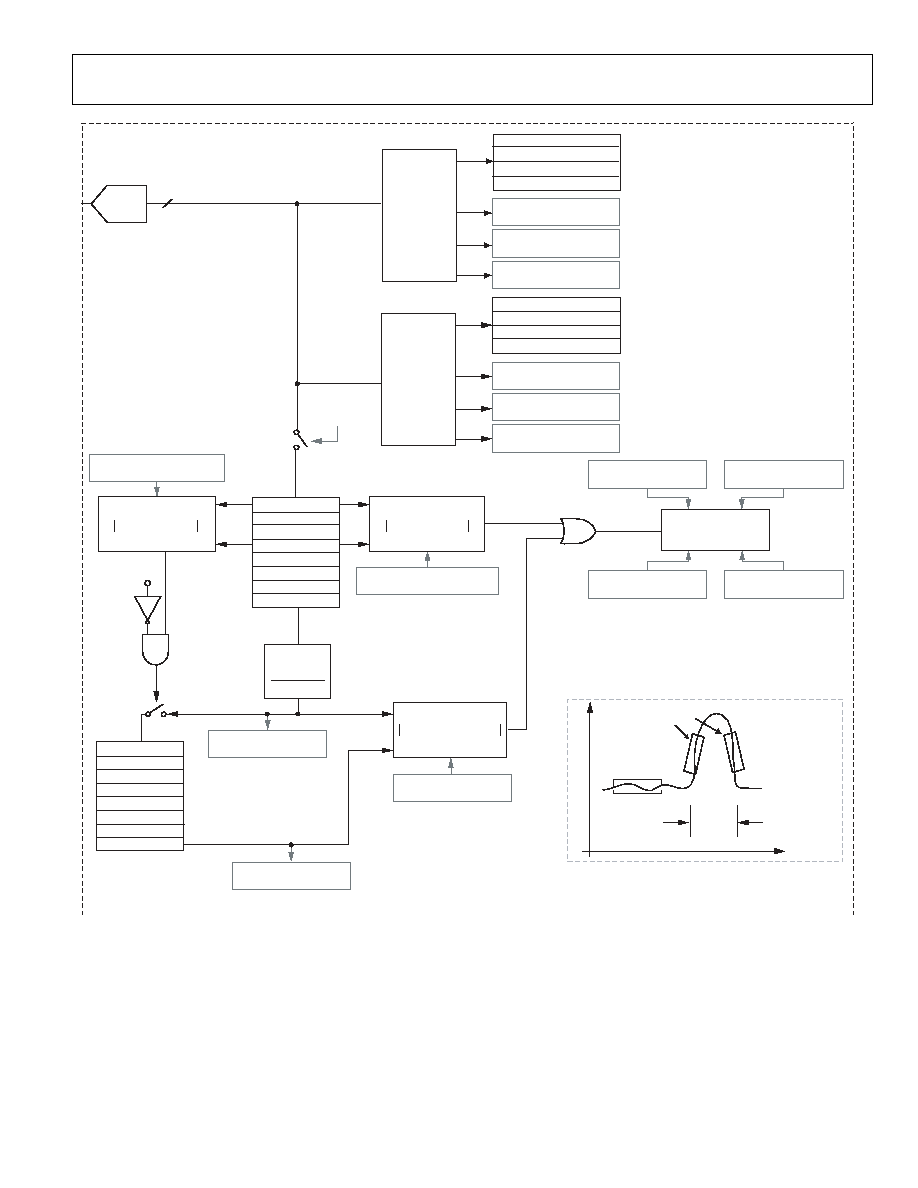
FIFO CONTROL
As shown in Figure 30, there are a number of FIFOs
implemented on the AD7142. These FIFOs are located in
Bank 3 of the on-chip memory. The FIFOs are used by the on-
chip logic to run the environmental calibration, adaptive
threshold, and proximity algorithms.
AVG_FP_SKIP and AVG_LP_SKIP
In Register 0x001, Bits[13:12]are the slow FIFO skip control for
full power mode, AVG_FP_SKIP. Bits[15:14] in the same
register are the slow FIFO skip control for low power mode,
AVG_LP_SKIP. These values determine which CDC samples
are not used (skipped) in the slow FIFO. Changing theses values
slows down or speeds up the rate at which the ambient
capacitance value tracks the measured capacitance value read by
the converter.
The slow FIFO is used by the on-chip logic to track the ambient
capacitance value. The slow FIFO expects to receive samples
from the converter at a rate of 33 ms to 40 ms. AVG_FP_SKIP
and AVG_LP_SKIP are used to normalize the frequency of the
samples going into the FIFO, regardless of how many
conversion stages are in a sequence.
Determining the AVG_FP_SKIP and AVG_LP_SKIP value is
only required once during the initial setup of the capacitance
sensor interface. Recommended values for these settings when
using all 12 conversion stages on the AD7142 are:
AVG_FP_SKIP = 11 = skip 31 samples
AVG_LP_SKIP = 11 = skip 3 samples
FF_SKIP_CNT
In Register 0x02, Bits[3:0] are the fast filter skip control,
FF_SKIP_CNT. This value determines which CDC samples are
not used (skipped) in the proximity detection fast FIFO.
The proximity detection fast FIFO is used by the on-chip logic
to determine if proximity is detected . The fast FIFO expects to
receive samples from the converter at a set rate. FF_SKIP_CNT
is used to normalize the frequency of the samples going into the
FIFO, regardless of how many conversion stages are in a
sequence.
Determining the FF_SKIP_CNT value is required only once
during the initial setup of the capacitance sensor interface.
Table 13 shows how FF_SKIP_CNT controls the update rate to
the fast FIFO. Recommended value for this setting when using
all 12 conversion stages on the AD7142 is:
FF_SKIP_CNT = 0000 = no samples skipped
Table 13. FF_SKIP_CNT Settings
FF_SKIP_CNT
FAST FIFO Update Rate
DECIMATION = 128
DECIMATION = 256
0
1.536 × (SEQUENCE_STAGE_NUM + 1) ms
3.072 × (SEQUENCE_STAGE_NUM + 1) ms
1
3.072 × (SEQUENCE_STAGE_NUM + 1) ms
6.144 × (SEQUENCE_STAGE_NUM + 1) ms
2
4.608 × (SEQUENCE_STAGE_NUM + 1) ms
9.216 × (SEQUENCE_STAGE_NUM + 1) ms
3
6.144 × (SEQUENCE_STAGE_NUM + 1) ms
12.288 × (SEQUENCE_STAGE_NUM + 1) ms
4
7.68 × (SEQUENCE_STAGE_NUM + 1) ms
15.36 × (SEQUENCE_STAGE_NUM + 1) ms
5
9.216 × (SEQUENCE_STAGE_NUM + 1) ms
18.432 × (SEQUENCE_STAGE_NUM + 1) ms
6
10.752 × (SEQUENCE_STAGE_NUM + 1) ms
21.504 × (SEQUENCE_STAGE_NUM + 1) ms
7
12.288 × (SEQUENCE_STAGE_NUM + 1) ms
24.576 × (SEQUENCE_STAGE_NUM + 1) ms
8
13.824 × (SEQUENCE_STAGE_NUM + 1) ms
27.648 × (SEQUENCE_STAGE_NUM + 1) ms
9
15.36 × (SEQUENCE_STAGE_NUM + 1) ms
30.72 × (SEQUENCE_STAGE_NUM + 1) ms
10
16.896 × (SEQUENCE_STAGE_NUM + 1) ms
33.792 × (SEQUENCE_STAGE_NUM + 1) ms
11
18.432 × (SEQUENCE_STAGE_NUM + 1) ms
36.864 × (SEQUENCE_STAGE_NUM + 1) ms
12
19.968 × (SEQUENCE_STAGE_NUM + 1) ms
39.936 × (SEQUENCE_STAGE_NUM + 1) ms
13
21.504 × (SEQUENCE_STAGE_NUM + 1) ms
43.008 × (SEQUENCE_STAGE_NUM + 1) ms
14
23.04 × (SEQUENCE_STAGE_NUM + 1) ms
46.08 × (SEQUENCE_STAGE_NUM + 1) ms
15
24.576 × (SEQUENCE_STAGE_NUM + 1) ms
49.152 × (SEQUENCE_STAGE_NUM + 1) ms
AD7142
Rev. 0 | Page 21 of 68
-
16-BIT
CDC
STAGE_FF_WORD0
8
7
N
= 0
PROXIMITY_DETECTION_RATE
REGISTER 0x003
PROXIMITY_RECAL_LVL
REGISTER 0x003
BANK 3 REGISTERS
PROXIMITY
AVERAGE AMBIENT
P
R
OX
IM
IT
Y
2
SLOW_FILTER_UPDATE_LVL
REGISTER 0x003
WORD0 WORD3
BANK 3 REGISTERS
SL
O
W
F
I
L
T
ER
EN
SW1
16
NOTES
1.
SLOW FILTER EN
IS SET AND SW1 IS CLOSED WHEN |WORD 0WORD 3| EXCEEDS THE VALUE PROGRAMMED IN THE SLOW_FILTER_UPDATE_LVL REGISTER PROVIDING
PROXIMITY
IS NOT SET.
2.
PROXIMITY 1
IS SET WHEN |WORD 0WORD 3| EXCEEDS THE VALUE PROGRAMMED IN THE PROXIMITY_DETECTION_RATE REGISTER.
3.
PROXIMITY 2
IS SET WHEN |AVERAGEAMBIENT| EXCEEDS THE VALUE PROGRAMMED IN THE PROXIMITY_RECAL_LVL REGISTER.
4. DESCRIPTION OF COMPARATOR FUNCTIONS:
COMPARATOR 1: USED TO DETECT WHEN A USER IS APPROACHING OR LEAVING A SENSOR.
COMPARATOR 2: USED TO DETECT WHEN A USER IS HOVERING OVER A SENSOR, OR APPROACHING A SENSOR VERY SLOWLY.
STAGE_SF_WORD0
SW
CONTROL
LOGIC
FP_PROXIMITY_RECAL
REGISTER 0x004
LP_PROXIMITY_RECAL
REGISTER 0X004
COMPARATOR 3
PROXIMITY
AMBIENT VALUE
STAGE_SF_WORDX
CDC O
UT
P
UT
CO
DE
TIME
SENSOR
CONTACT
STAGE_SF_AMBIENT
BANK 3 REGISTERS
STAGE_FF_AVG
BANK 3 REGISTERS
STAGE_MAX_WORD0
STAGE_MAX_WORD1
STAGE_MAX_WORD2
STAGE_MAX_WORD3
STAGE_MAX_AVG
BANK 3 REGISTERS
STAGE_HIGH_THRESHOLD
BANK 3 REGISTERS
STAGE_MAX_TEMP
BANK 3 REGISTERS
MAX LEVEL
DETECTION
LOGIC
BANK 3 REGISTERS
STAGE_MIN_WORD0
STAGE_MIN_WORD1
STAGE_MIN_WORD2
STAGE_MIN_WORD3
STAGE_MIN_AVG
BANK 3 REGISTER3
STAGE_LOW_THRESHOLD
BANK 3 REGISTERS
STAGE_MIN_TEMP
BANK 3 REGISTERS
MIN LEVEL
DETECTION
LOGIC
BANK 3 REGISTERS
FP_PROXIMITY_CNT
REGISTER 0x002
LP_PROXIMITY_CNT
REGISTER 0X002
PROXIMITY 1
PROXIMITY TIMING
CONTROL LOGIC
COMPARATOR 1
COMPARATOR 2
WORD(
N
)
05702-
021
STAGE_SF_WORD2
STAGE_SF_WORD1
STAGE_SF_WORD4
STAGE_SF_WORD3
STAGE_SF_WORD5
STAGE_SF_WORD7
STAGE_SF_WORD6
STAGE_FF_WORD7
STAGE_FF_WORD6
STAGE_FF_WORD5
STAGE_FF_WORD4
STAGE_FF_WORD3
STAGE_FF_WORD2
STAGE_FF_WORD1
STAGE_FF_WORDX
ALSO USED TO DETECT IF THE SENSOR AMBIENT LEVEL HAS CHANGED AS A RESULT OF THE USER INTERACTION.
FOR EXAMPLE, HUMIDITY OR DIRT LEFT BEHIND ON SENSOR.
COMPARATOR 3: USED TO ENABLE THE SLOW FILTER UPDATE RATE. THE SLOW FILTER IS UPDATED WHEN
SLOW FILTER EN
IS SET AND
PROXIMITY
IS NOT SET.
WORD0 WORD3
Figure 30. AD7142 Proximity Detection and Environmental Calibration
AD7142
Rev. 0 | Page 22 of 68
ENVIRONMENTAL CALIBRATION
The AD7142 provides on-chip capacitance sensor calibration to
automatically adjust for environmental conditions that have an
effect on the capacitance sensor ambient levels. Capacitance
sensor output levels are sensitive to temperature, humidity, and
in some cases, dirt. The AD7142 achieves optimal and reliable
sensor performance by continuously monitoring the CDC
ambient levels and correcting for any changes by adjusting the
STAGE_HIGH_THRESHOLD and STAGE_LOW_
THRESHOLD register values. The CDC ambient level is
defined as the capacitance sensor output level during periods
when the user is not approaching or in contact with the sensor.
The compensation logic runs automatically on every conversion
after configuration when the AD7142 is not being touched. This
allows the AD7142 to account for rapidly changing environ-
mental conditions.
The ambient compensation control registers give the host access
to general setup and controls for the compensation algorithm.
The RAM stores the compensation data for each conversion
stage, as well as setup information specific to each stage.
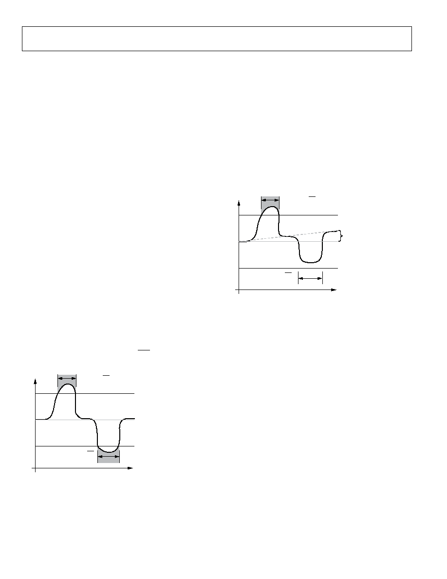
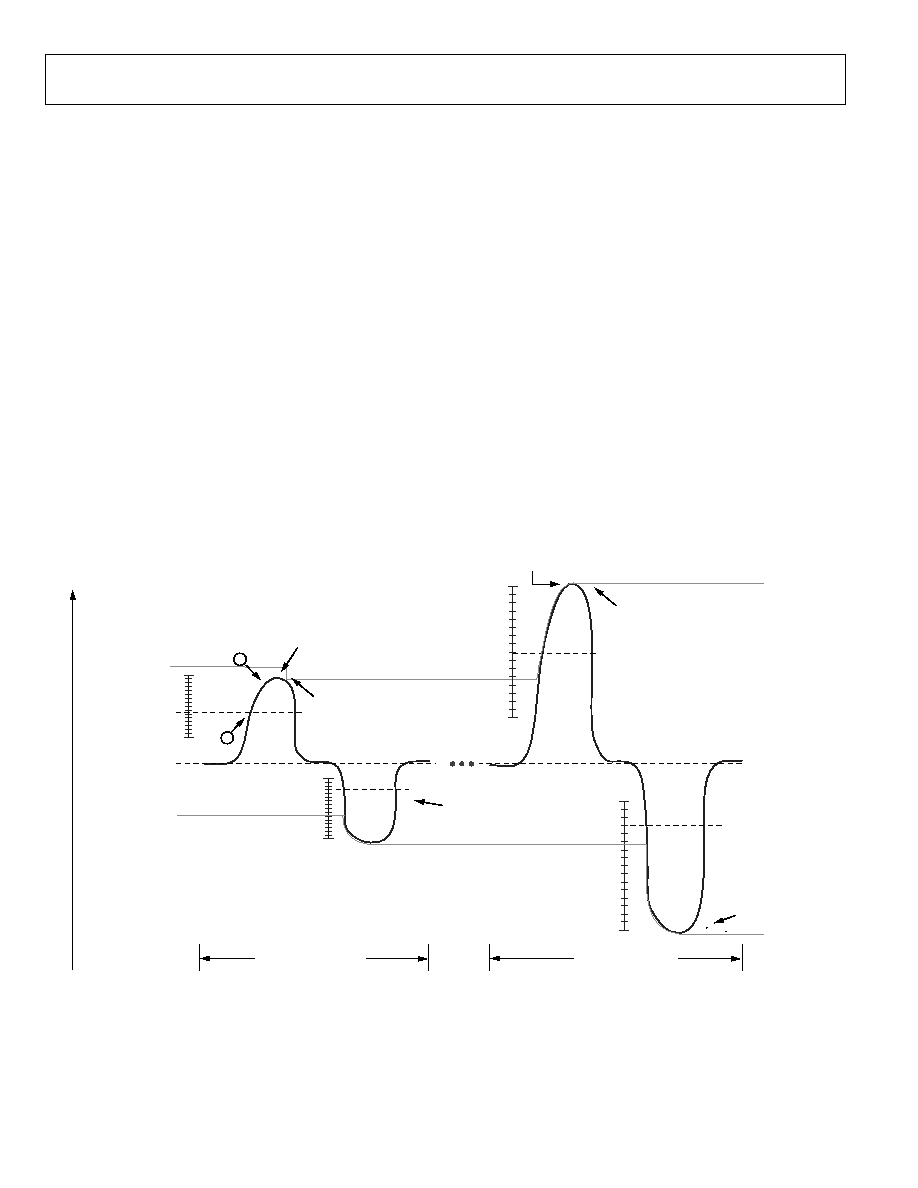
Figure 31 shows an example of an ideal capacitance sensor
behavior where the CDC ambient level remains constant
regardless of the environmental conditions. The CDC output
shown is for a pair of differential button sensors, where one
sensor caused an increase, and the other a decrease in measured
capacitance when activated. The positive and negative sensor
threshold levels are calculated as a percentage of the
STAGE_OFFSET_HIGH and STAGE_OFFSET_LOW values
based on the threshold sensitivity settings and the ambient
value. These values are sufficient to detect a sensor contact,
resulting with the AD7142 asserting the INT output when the
threshold levels are exceeded.
CD
C O
U
T
P
UT
CO
DE
S
t
STAGE_LOW_THRESHOLD
STAGE_HIGH_THRESHOLD
CDC AMBIENT VALUE
CHANGING ENVIRONMENTAL CONDITIONS
0
570
2-
0
22
SENSOR 1 INT
ASSERTED
SENSOR 2 INT
ASSERTED
Figure 31. Ideal Sensor Behavior with a Constant Ambient Level
CAPACITANCE SENSOR BEHAVIOR WITHOUT
CALIBRATION
Figure 32 shows the typical behavior of a capacitance sensor
with no applied calibration. This figure shows ambient levels
drifting over time as environmental conditions change. The
ambient level drift has resulted in the detection of a missed user
contact on Sensor 2. This is a result of the initial low offset level
remaining constant while the ambient levels drifted upward
beyond the detection range.
The Capacitance Sensor Behavior with Calibration section
describes how the AD7142 adaptive calibration algorithm
prevents errors such as this from occurring.
CDC
O
U
T
P
UT
CO
DE
S
t
CCDC AMBIENT
VALUE DRIFTING
SENSOR 1 INT
ASSERTED
SENSOR 2 INT
NOT ASSERTED
CHANGING ENVIRONMENTAL CONDITIONS
STAGE_HIGH_THRESHOLD
STAGE_LOW_THRESHOLD
05
70
2-
02
3
Figure 32. Typical Sensor Behavior Without Calibration Applied
AD7142
Rev. 0 | Page 23 of 68
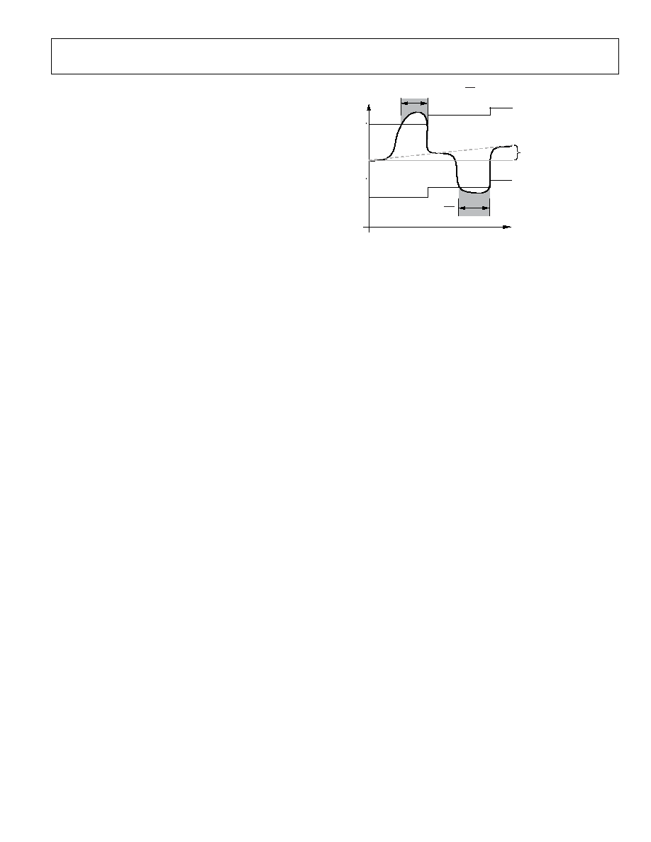
CAPACITANCE SENSOR BEHAVIOR WITH
CALIBRATION
The AD7142 on-chip adaptive calibration algorithm prevents
sensor detection errors such as the one shown in Figure 32. This
is achieved by monitoring the CDC ambient levels and
internally adjusting the initial offset level register values
according to the amount of ambient drift measured on each
sensor. This closed loop routine ensures the reliability and
repeatable operation of every sensor connected to the AD7142
under dynamic environmental conditions. Figure 33 shows a
simplified example of how the AD7142 applies the adaptive
calibration process resulting in no interrupt errors under
changing CDC ambient levels due to environmental conditions.
C
DC O
UT
P
UT
C
O
D
E
S
t
SENSOR 1 INT
ASSERTED
1
2
3
4
5
6
STAGE_HIGH_THRESHOLD
(POST CALIBRATED
REGISTER VALUE)
05
70
2-
02
4
CHANGING ENVIRONMENTAL CONDITIONS
NOTES
1. INITIAL STAGE_OFFSET_HIGH REGISTER VALUE
2. POST CALIBRATED REGISTER STAGE_HIGH_THRESHOLD
3. POST CALIBRATED REGISTER STAGE_HIGH_THRESHOLD
4. INITIAL STAGE_LOW_THRESHOLD
5. POST CALIBRATED REGISTER STAGE_LOW_THRESHOLD
6. POST CALIBRATED REGISTER STAGE_LOW_THRESHOLD
CDCAMBIENT
VALUE DRIFTING
STAGE_LOW_THRESHOLD
(POST CALIBRATED
REGISTER VALUE)
SENSOR 2 INT
ASSERTED
Figure 33. Typical Sensor Behavior with Calibration Applied on the Data Path
AD7142
Rev. 0 | Page 24 of 68
ADAPTIVE THRESHOLD AND SENSITIVITY
The AD7142 provides an on-chip self-learning adaptive
threshold and sensitivity algorithm. This algorithm continu-
ously monitors the output levels of each sensor and automatically
rescales the threshold levels proportionally to the sensor area
covered by the user. As a result, the AD7142 maintains optimal
threshold and sensitivity levels for all types of users regardless
of their finger sizes.
The threshold level is always referenced from the ambient level
and is defined as the CDC converter output level that must be
exceeded for a valid sensor contact. The sensitivity level is
defined as how sensitive the sensor is before a valid contact is
registered.
Figure 34 provides an example of how the adaptive threshold and
sensitivity algorithm works. The positive and negative sensor
threshold levels are calculated as a percentage of the
STAGE_OFFSET_HIGH and STAGE_OFFSET_LOW values
based on the threshold sensitivity settings and the ambient value.
On configuration, initial estimates are supplied for both
STAGE_OFFSET_HIGH and STAGE_OFFSET_LOW after which
the calibration engine automatically adjusts the
STAGE_HIGH_THRESHOLD and STAGE_LOW _THRESHOLD
values for sensor response.
Reference A in Figure 34 shows an under sensitive threshold
level for a small finger user, demonstrating the disadvantages of
a fixed threshold level. By enabling the adaptive threshold and
sensitivity algorithm, the positive and negative threshold levels
are determined by the POS_ THRESHOLD_SENSITIVITY and
NEG_THRESHOLD_ SENSITIVITY register values and the
most recent average maximum sensor output value. These
registers can be used to select 16 different positive and negative
sensitivity levels ranging between 25% and 95.32% of the most
recent average maximum output level referenced from the
ambient value. The smaller the sensitivity percentage setting,
the easier it is to trigger a sensor activation. Reference B shows
that the positive adaptive threshold level is set at almost mid-
sensitivity with a 62.51% threshold level by setting
POS_THRESHOLD_ SENSITIVITY = 1000. Figure 34 also
provides a similar example for the negative threshold level with
NEG_ THRESHOLD_SENSITIVITY = 0001.
AMBIENT LEVEL
CDC O
UT
P
UT
CO
DES
AVERAGE MAX VALUE
STAGE_OFFSET_HIGH
25%
95.32%
62.51% = POS
ADAPTIVE
THRESHOLD LEVEL
25%
62.51% = POS ADAPTIVE
THRESHOLD LEVEL
95.32%
NEG ADAPTIVE THRESHOLD LEVEL = 39.08%
25%
95.32%
25%
95.32%
SENSOR CONTACTED
BY SMALL FINGER
AVERAGE MAX VALUE
STAGE_OFFSET_LOW
NEG ADAPTIVE THRESHOLD LEVEL = 39.08%
SENSOR CONTACTED
BY LARGE FINGER
05
702-
025
STAGE_OFFSET_HIGH
IS UPDATED
STAGE_OFFSET_HIGH
IS UPDATED HERE
STAGE_OFFSET_LOW
IS UPDATED HERE
STAGE_OFFSET_LOW
IS UPDATED HERE
A
B
Figure 34. Threshold Sensitivity Example with POS_THRESHOLD_SENSITIVITY = 1000 and NEG_THRESHOLD_SENSITIVITY = 0011
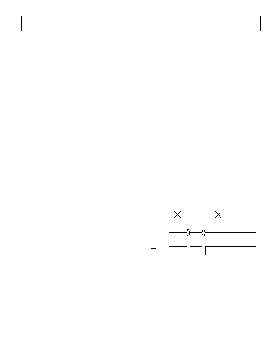
AD7142
Rev. 0 | Page 25 of 68
INTERRUPT OUTPUT
The AD7142 has an interrupt output that triggers an interrupt
service routine on the host processor. The INT signal is on
Pin 25, and is an open-drain output. There are three types of
interrupt events on the AD7142: a CDC conversion complete
interrupt, a sensor threshold interrupt, and a GPIO interrupt.
Each interrupt has enable and status registers. The conversion
complete and sensor threshold interrupts can be enabled on a
per conversion stage basis. The status registers indicate what
type of interrupt triggered the INT pin. Status registers are
cleared, and the INT signal is reset high, during a read
operation. The signal returns high as soon as the read address
has been set up.
CDC CONVERSION COMPLETE INTERRUPT
The AD7142 interrupt signal asserts low to indicate the
completion of a conversion stage, and new conversion result
data is available in the registers.
The interrupt can be independently enabled for each conversion
stage. Each conversion stage complete interrupt can be enabled via
the STAGE_COMPLETE_EN register (Address 0x007). This
register has a bit that corresponds to each conversion stage. Setting
this bit to 1 enables the interrupt for that stage. Clearing this bit to 0
disables the conversion complete interrupt for that stage.
In normal operation, the AD7142's interrupt is enabled only for the
last stage in a conversion sequence. For example, if there are five
conversion stages, the conversion complete interrupt for STAGE4 is
enabled. INT only asserts when all five conversion stages are
complete, and the host can read new data from all five result
registers. The interrupt is cleared by reading the
STAGE_COMPLETE_STATUS_INT register located at Address
0x00A.
Register 0x00A is the conversion complete interrupt status
register. Each bit in this register corresponds to a conversion
stage. If a bit is set, it means that the conversion complete
interrupt for the corresponding stage was triggered. This
register is cleared on a read, provided the underlying condition
that triggered the interrupt has gone away.
SENSOR TOUCH INTERRUPT
The sensor touch interrupt mode is implemented when the host
processor requires an interrupt only when a sensor is contacted.
Configuring the AD7142 into this mode results in the interrupt
being asserted when the user makes contact with the sensor and
again when the user lifts off the sensor. The second interrupt is
required to alert the host processor that the user is no longer
contacting the sensor.
The registers located at Address 0x005 and Address 0x006 are
used to enable the interrupt output for each stage. The registers
located at Address 0x008 and Address 0x009 are used to read
back the interrupt status for each stage.
Figure 35 shows the interrupt output timing during contact with
one of the sensors connected to STAGE0 while operating in the
sensor touch interrupt mode. For a low limit configuration, the
interrupt output is asserted as soon as the sensor is contacted and
again after the user has stopped contacting the sensor.
Note: The interrupt output remains low until the host processor
reads back the interrupt status registers located at Address
0x008 and Address 0x009.
The interrupt output is asserted when there is a change in the
threshold status bits. This could indicate that a user is now
touching the sensor(s) for the first time, the number of sensors
being touched has changed, or the user is no longer touching
the sensor(s). Reading the status bits in the interrupt status
register shows the current sensor activations.
4
2
CONVERSION
STAGE
SERIAL
READ BACK
NOTES:
1. USER TOUCHING DOWN ON SENSOR
2. ADDRESS 0X008 READ BACKTO CLEAR INTERRUPT
3. USER LIFTING OFF OF SENSOR
4. ADDRESS 0X008 READ BACK TO CLEAR INTERRUPT
STAGE0
STAGE1
INT OUTPUT
05702-
055
Figure 35. Example of Sensor Touch Interrupt
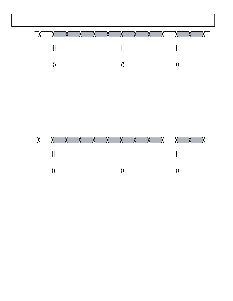
AD7142
Rev. 0 | Page 26 of 68
STAGE0
STAGE1
STAGE2
STAGE3
STAGE4
STAGE5
STAGE6
STAGE7
STAGE8
STAGE9
STAGE10
STAGE11
2
3
1
INT
CONVERSIONS
SERIAL
READS
NOTES
THIS IS AN EXAMPLE OF A CDC CONVERSION COMPLETE INTERRUPT.
THIS TIMING EXAMPLE SHOWS THAT THE INTERRUPT OUTPUT HAS BEEN ENABLED TO BE ASSERTED AT THE END OF A CONVERSION CYCLE FOR
STAGE0, STAGE5, AND STAGE9. THE INTERRUPTS FOR ALL OTHER STAGES HAVE BEEN DISABLED.
STAGEx CONFIGURATION PROGRAMMING NOTES FOR STAGE0, STAGE5, AND STAGE9 (x = 0, 5, 9)
STAGEx_LOW_INT_EN (ADDRESS 0x005) = 0
STAGEx_HIGH_INT_EN (ADDRESS 0x006) = 0
STAGEx_COMPLETE_EN (ADDRESS 0x007) = 1
STAGEx CONFIGURATION PROGRAMMING NOTES FOR STAGE 1 THROUGH STAGE 8, STAGE10, AND STAGE11 (x = 1, 2, 3, 4, 5, 6, 7, 8, 10, 11)
STAGEx_LOW_INT_EN (ADDRESS 0x005) = 0
STAGEx_HIGH_INT_EN (ADDRESS 0x006) = 0
STAGEx_COMPLETE_EN (ADDRESS 0x007) = 0
SERIAL READBACK REQUIREMENTS FOR STAGE0, STAGE5 AND STAGE9. THIS READBACK OPERATION IS REQUIRED TO CLEAR THE INTERRUPT OUTPUT.
1. READ THE STAGE0_COMPLETE_STATUS_INT (ADDRESS 0x00A) REGISTER
2. READ THE STAGE5_COMPLETE_STATUS_INT (ADDRESS 0x00A) REGISTER
3. READ THE STAGE9_COMPLETE_STATUS_INT (ADDRESS 0x00A) REGISTER
05
702-
0
26
Figure 36. Example of Configuring the Registers for End of Conversion Interrupt Setup
05702-
027
4
2
1
INT
CONVERSIONS
SERIAL
READS
NOTES
THIS IS AN EXAMPLE OF A SENSOR THRESHOLD INTERRUPT FOR A CASE WHERE THE LOW THRESHOLD LEVELS WERE EXCEEDED.
FOR EXAMPLE: THE SENSOR CONNECTED TO STAGE0 AND STAGE9 WERE CONTACTED AND THE LOW THRESHOLD LEVELS WERE EXCEEDED RESULTING
IN THE INTERRUPT BEING ASSERTED. THE STAGE6 INTERRUPT WAS NOT ASSERTED BECAUSE THE USER DID NOT CONTACT THE SENSOR CONNECTED TO
STAGE6.
STAGEx CONFIGURATION PROGRAMMING NOTES FOR STAGE 0, STAGE6, AND STAGE9 (x = 0, 6, 9)
STAGEx_LOW_INT_EN (ADDRESS 0x005) = 1
STAGEx_HIGH_INT_EN (ADDRESS 0x006) = 0
STAGEx_COMPLETE_EN (ADDRESS 0x007) = 0
STAGEx CONFIGURATION PROGRAMMING NOTES FOR STAGE 1 THROUGH STAGE7, STAGE8, STAGE10, AND STAGE11 (x = 1, 2, 3, 4, 5, 6, 7, 8, 10, 11)
STAGEx_LOW_INT_EN (ADDRESS 0x005) = 0
STAGEx_HIGH_INT_EN (ADDRESS 0x006) = 0
STAGEx_COMPLETE_EN (ADDRESS 0x007) = 0
SERIAL READBACK REQUIREMENTS FOR STAGE0 AND STAGE9. THIS READBACK OPERATION IS REQUIRED TO CLEAR THE INTERRUPT OUTPUT.
1. READ THE STAGE0_LOW_LIMIT_INT (ADDRESS 0x008) REGISTER
2. READ THE STAGE5_LOW_LIMIT_INT (ADDRESS 0x008) REGISTER
STAGE0
STAGE1
STAGE2
STAGE3
STAGE4
STAGE5
STAGE6
STAGE7
STAGE8
STAGE9
STAGE10
STAGE11
Figure 37. Example of Configuring the Registers for Sensor Interrupt Setup
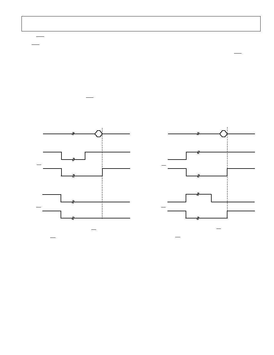
AD7142
Rev. 0 | Page 27 of 68
GPIO INT OUTPUT CONTROL
The INT output signal can be controlled by the GPIO pin when
the GPIO is configured as an input. The GPIO is configured as
an input by setting the GPIO_SETUP bits in the interrupt
configuration register to 01. See the GPIO section for more
information on how to configure the GPIO.
Enable the GPIO interrupt by setting the GPIO_INT_EN bit in
Register 0x007 to 1, or disable the GPIO interrupt by clearing this
bit to 0. The GPIO status bit in the conversion complete interrupt
status register reflects the status of the GPIO interrupt. This bit is
set to 1 when the GPIO has triggered INT. The bit is cleared on
readback from the register, provided the condition that caused
the interrupt has gone away.
The GPIO interrupt can be set to trigger on a rising edge, falling
edge, high level, or low level at the GPIO input pin. Table 14
shows how the settings of the GPIO_INPUT_CONFIG bits in
the interrupt enable register affect the behavior of INT.
Figure 38 to Figure 41 show how the interrupt output is cleared
on a read from the CDC conversion complete interrupt status
register.
GPIO
INPUT
INT
OUTPUT
SERIAL
READBACK
GPIO
INPUT
INT
OUTPUT
1
NOTES
1. READ GPIO_STATUS REGISTER TO RESET INT OUTPUT.
GPIO INPUT HIGH WHEN REGISTER IS READ BACK
GPIO INPUT LOW WHEN REGISTER IS READ BACK
057
02
-
028
Figure 38. INT Output Controlled by the GPIO Input Example,
GPIO_SETUP = 01, GPIO_INPUT_CONFIG = 00
GPIO
INPUT
INT
OUTPUT
SERIAL
READBACK
GPIO
INPUT
INT
OUTPUT
1
GPIO INPUT HIGH WHEN REGISTER IS READ BACK
GPIO INPUT LOW WHEN REGISTER IS READ BACK
NOTES
1. READ GPIO_STATUS REGISTER TO RESET INT OUTPUT.
0
570
2-
02
9
Figure 39. INT Output Controlled by the GPIO Input Example,
GPIO_SETUP = 01, GPIO_INPUT_CONFIG = 01
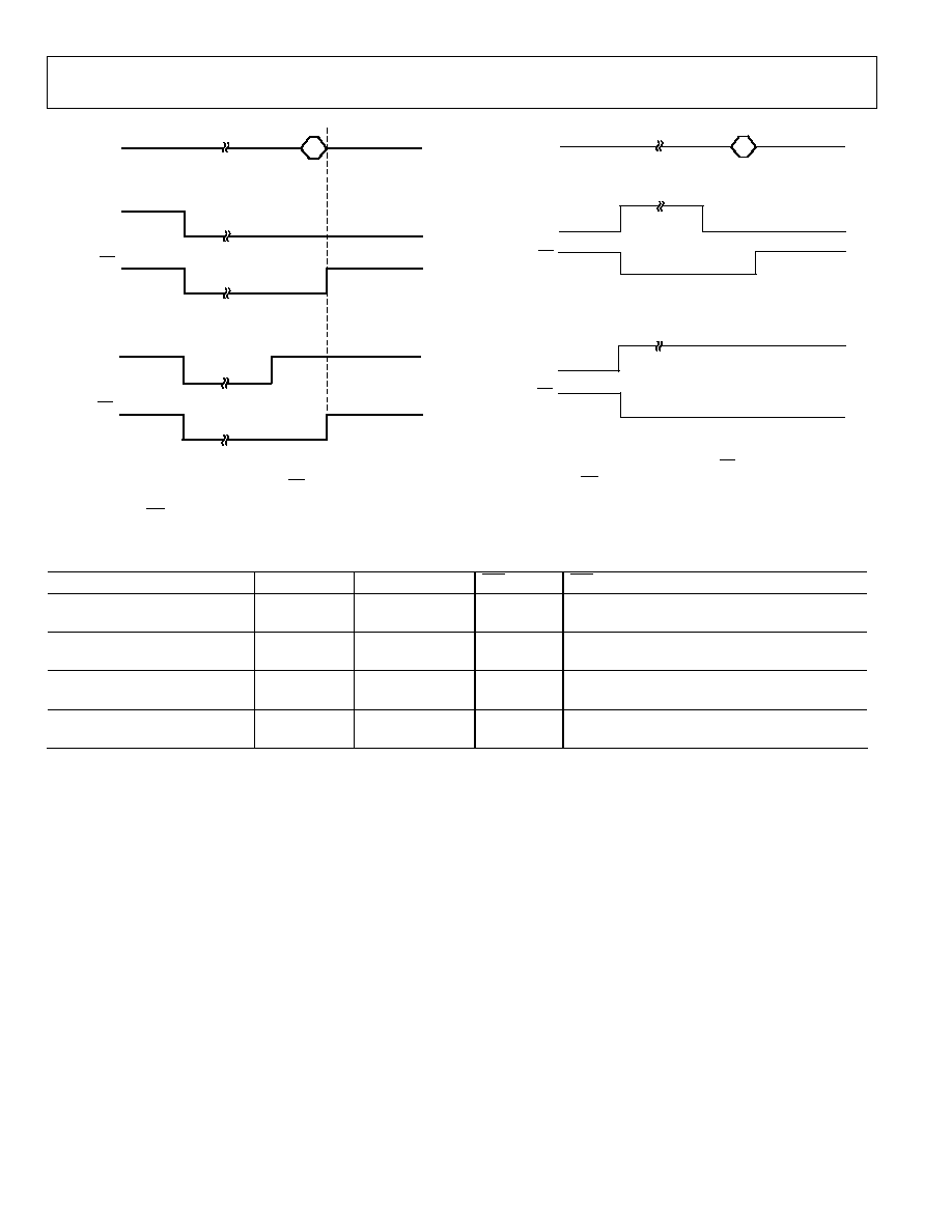
AD7142
Rev. 0 | Page 28 of 68
GPIO
INPUT
INT
OUTPUT
SERIAL
READBACK
GPIO
INPUT
INT
OUTPUT
1
GPIO INPUT LOW WHEN REGISTER IS READBACK
GPIO INPUT HIGH WHEN REGISTER IS READBACK
NOTES
1. READ GPIO_STATUS REGISTER TO RESET INT OUTPUT.
05
702-
0
30
Figure 40. INT Output Controlled by the GPIO Input Example,
GPIO_SETUP = 01, GPIO_INPUT_CONFIG = 10
GPIO
INPUT
INT
OUTPUT
SERIAL
READBACK
GPIO
INPUT
INT
OUTPUT
1
GPIO INPUT LOW WHEN REGISTER IS READBACK
GPIO INPUT HIGH WHEN REGISTER IS READBACK
NOTES
1. READ GPIO_STATUS REGISTER TO RESET INT OUTPUT.
05
70
2-
03
1
Figure 41. INT Output Controlled by the GPIO Input Example,
GPIO_SETUP = 01, GPIO_INPUT_CONFIG = 11
Table 14. GPIO Interrupt Behavior
GPIO_INPUT_CONFIG
GPIO Pin
GPIO_STATUS
INT
INT Behavior
00 = Negative Level Triggered
1
0
1
Not triggered
00 = Negative Level Triggered
0
1
0
Asserted while signal on GPIO pin is low
01 = Positive Edge Triggered
1
1
0
Pulses low at low-to-high GPIO transition
01 = Positive Edge Triggered
0
0
1
Not triggered
10 = Negative Edge Triggered
1
0
1
Pulses low at high-to-low GPIO transition
10 = Negative Edge Triggered
0
1
0
Not triggered
11 = Positive Level Triggered
1
1
0
Asserted while signal on GPIO pin is high
11 = Positive Level Triggered
0
0
1
Not triggered
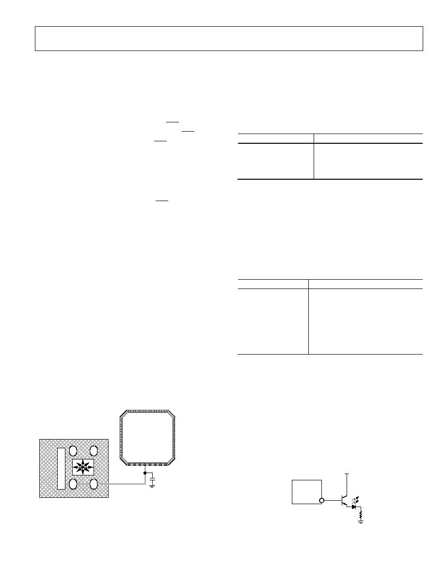
AD7142
Rev. 0 | Page 29 of 68
OUTPUTS
EXCITATION SOURCE
The excitation source on board the AD7142 is a square wave
source with a frequency of 240 kHz. This excitation source
forms the electric field between the transmitter and receiver in
the external capacitance sensor PCB. The source is output from
the AD7142 on two pins, the SRC pin and the SRC pin (outputs
an inverted version of the source square wave). The SRC signal
offsets large external sensor capacitances. SRC is not used in the
majority of applications.
The source output can be disabled from both output pins
separately by writing to the control register bits (Address
0x000[13:12]). Setting Bit 12 in this register to 1 disables the
source output on the SRC pin. Setting Bit 13 in this register to 1
disables the inverted source output on the SRC pin.
C
SHIELD
OUTPUT
To prevent leakage from the external capacitance sensors, the
sensor traces are shielded. The AD7142 has a voltage output
that can be used as the potential for any shield traces, C
SHIELD
.
The C
SHIELD
voltage is equal to AV
DD
/2.
The C
SHIELD
potential is derived from the output of the AD7142
internal amplifier, and is of equal potential to the CIN input
lines. Because the shield is at the same potential as the sensor
traces, no leakage to ground occurs. To eliminate any ringing on
the C
SHIELD
output, connect a 10 nF capacitor between the
C
SHIELD
pin and ground.
For 4-layer sensors, C
SHIELD
is connected to a copper plane
around the sensors on layers 2, 3, and 4. A ground copper plane
is used on Layer 1 around the source electrodes. On a 2-layer
sensor, C
SHIELD
is connected to a copper plane around the
sensors on the bottom layer. A ground copper plane is used on
the top layer around the source electrodes.
Figure 42 shows how the sensor traces are shielded by running
traces connected to the shield potential around the sensor traces.
C
SH
I
EL
D
05
70
2-
0
32
10nF
SE
N
SO
R
P
C
B
AD7142
Figure 42. Shielding the Sensor Traces
GPIO
The AD7142 has one GPIO pin located at Pin 26. It can be
configured as an input or an output. The GPIO_SETUP Bits[13:12]
in the interrupt enable register determine how the GPIO pin is
configured.
Table 15. GPIO_SETUP Bits
GPIO_SETUP GPIO
Configuration
00 GPIO
disabled
01 Input
10 Output
low
11 Output
high
When the GPIO is configured as an output, the voltage level on
the pin is set to either a low level or a high level, as defined by
the GPIO_SETUP bits shown in Table 15.
When the GPIO is configured as an input, the
GPIO_INPUT_CONFIG bits in the interrupt enable register
determine the response of the AD7142 to a signal on the GPIO
pin. The GPIO can be configured as either active high or active
low, as well as either edge triggered or level triggered, as listed
in Table 16.
Table 16. GPIO_INPUT_CONFIG Bits
GPIO_INPUT_CONFIG GPIO
Configuration
00
Triggered on negative level
(active low)
01
Triggered on positive edge
(active high)
10
Triggered on negative edge
(active low)
11
Triggered on positive level
(active high)
When GPIO is configured as an input, it triggers the interrupt
output on the AD7142. Table 14 lists the interrupt output
behavior for each of the GPIO configuration setups.
USING THE GPIO TO TURN ON/OFF AN LED
The GPIO on the AD7142 can be used to turn on and off LEDs
by setting the GPIO as either output high or low. Setting the
GPIO output high turns on the LED; setting the GPIO output
low turns off the LED. The GPIO pin connects to a transistor
that provides the drive current for the LED. Suitable transistors
include the KTC3875.
AD7142
GPIO
V
CC
KTC3875
OR SIMILAR
05
70
2-
0
6
1
Figure 43. Controlling LEDs Using the GPIO
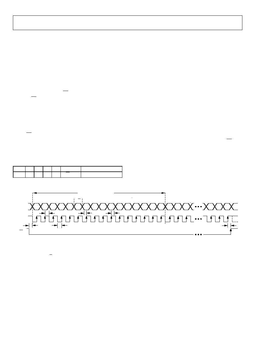
AD7142
Rev. 0 | Page 30 of 68
SERIAL INTERFACE
The AD7142 is available with an SPI serial interface. The
AD7142-1 is available with an I
2
C-compatible interface. Both
parts are the same, with the exception of the serial interface.
SPI INTERFACE
The AD7142 has a 4-wire serial peripheral interface (SPI). The
SPI has a data input pin (SDI) for inputting data to the device, a
data output pin (SDO) for reading data back from the device,
and a data clock pin (SCLK) for clocking data into and out of
the device. A chip select pin (CS) enables or disables the serial
interface. CS is required for correct operation of the SPI
interface. Data is clocked out of the AD7142 on the negative
edge of SCLK, and data is clocked into the device on the
positive edge of SCLK.
SPI Command Word
All data transactions on the SPI bus begin with the master
taking CS from high to low and sending out the command
word. This indicates to the AD7142 whether the transaction is a
read or a write, and gives the address of the register from which
to begin the data transfer. The following bit map shows the SPI
command word.
MSB
LSB
15 14 13 12 11 10
9:0
1 1 1 0 0 R/W
Register address
Bits[15:11] of the command word must be set to 11100 to
successfully begin a bus transaction.
Bit 10 is the read/write bit; 1 indicates a read, and 0 indicates a
write.
Bits[9:0] contain the target register address. When reading or
writing to more than one register, this address indicates the
address of the first register to be written to or read from.
Writing Data
Data is written to the AD7142 in 16-bit words. The first word
written to the device is the command word, with the read/write
bit set to 0. The master then supplies the 16-bit input data-word
on the SDI line. The AD7142 clocks the data into the register
addressed in the command word. If there is more than one
word of data to be clocked in, the AD7142 automatically incre-
ments the address pointer, and clocks the next data-word into
the next register.
The AD7142 continues to clock in data on the SDI line until
either the master finishes the write transition by pulling CS
high, or until the address pointer reaches its maximum value.
The AD7142 address pointer does not wrap around. When it
reaches its maximum value, any data provided by the master on
the SDI line is ignored by the AD7142.
NOTES
1. SDI BITS ARE LATCHED ON SCLK RISING EDGES. SCLK CAN IDLE HIGH OR LOW BETWEEN WRITE OPERATIONS.
2. ALL 32 BITS MUST BE WRITTEN: 16 BITS FOR CONTROL WORD AND 16 BITS FOR DATA.
3. 16-BIT COMMAND WORD SETTINGS FOR SERIAL WRITE OPERATION:
CW[15:11] = 11100 (ENABLE WORD)
CW[10] = 0 (R/W)
CW[9:0] = [AD9, AD8, AD7, AD6, AD5, AD4, AD3, AD2, AD1, AD0] (10-BIT MSB JUSTIFIED REGISTER ADDRESS)
CW
11
CW
10
CW
13
CW
12
SDI
CW
15
CW
14
CW
9
CW
7
CW
6
CW
5
CW
4
CW
3
CW
2
CW
1
CW
0
D2
D1
D0
CW
8
t
1
t
4
16-BIT COMMAND WORD
16-BIT DATA
5
32
6
7
8
9
10
11
12
13
14
15
16
30
31
t
8
t
5
SCLK
1
2
3
4
D15
D14
D13
17
18
19
CS
ENABLE WORD
R/W
REGISTER ADDRESS
t
2
t
3
057
02-
033
Figure 44. Single Register Write SPI Timing
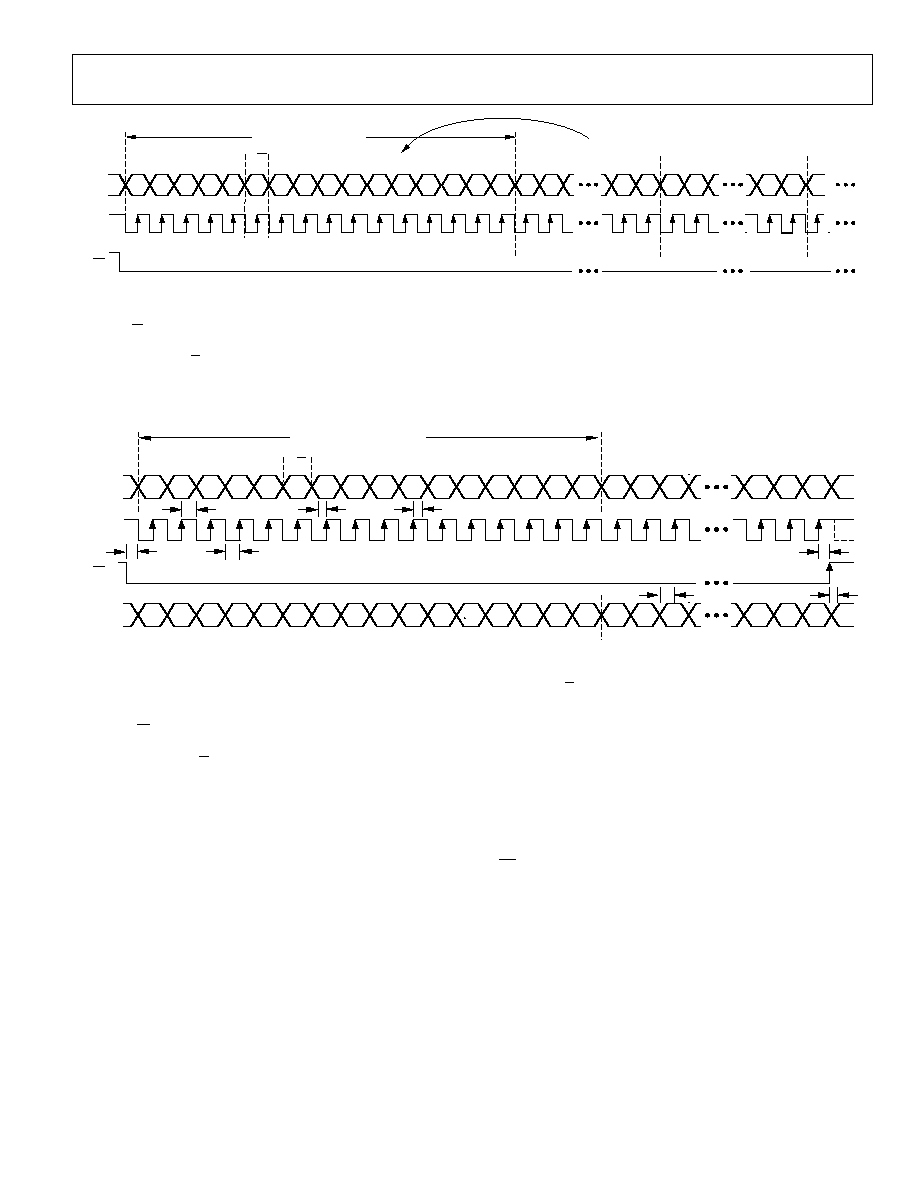
AD7142
Rev. 0 | Page 31 of 68
SDI
CW
15
CW
14
CW
13
CW
8
CW
1
CW
0
D15
D14
SCLK
CW
12
NOTES
1. MULTIPLE SEQUENTIAL REGISTERS CAN BE LOADED CONTINUOUSLY.
2. THE FIRST (LOWEST ADDRESS) REGISTER ADDRESS IS WRITTEN, FOLLOWED BY MULTIPLE 16-BIT DATA-WORDS.
3. THE ADDRESS AUTOMATICALLY INCREMENTS WITH EACH 16-BIT DATA-WORD (ALL 16 BITS MUST BE WRITTEN).
4. CS IS HELD LOW UNTIL THE LAST DESIRED REGISTER HAS BEEN LOADED.
5. 16-BIT COMMAND WORD SETTINGS FOR SEQUENTIAL WRITE OPERATION:
CW[15:11] = 11100 (ENABLE WORD)
CW[10] = 0 (R/W)
CW[9:0] = [AD9, AD8, AD7, AD6, AD5, AD4, AD3, AD2, AD1, AD0] (STARTING MSB JUSTIFIED REGISTER ADDRESS)
D1
D0
D1
D0
D15
DATA FOR STARTING
REGISTER ADDRESS
DATA FOR NEXT
REGISTER ADDRESS
D15
D14
1
32
2
3
4
15
16
17
18
31
34
33
48
47
49
CS
CW
11
CW
10
CW
9
CW
7
CW
2
CW
6
CW
5
CW
4
CW
3
11
12
13
14
5
6
7
8
9
10
16-BIT COMMAND WORD
ENABLE WORD
R/W
STARTING REGISTER ADDRESS
05702-
034
Figure 45. Sequential Register Write SPI Timing
NOTES
1. SDI BITS ARE LATCHED ON SCLK RISING EDGES. SCLK CAN IDLE HIGH OR LOW BETWEEN WRITE OPERATIONS.
2. THE 16-BIT CONTROL WORD MUST BE WRITTEN ON SDI: 5 BITS FOR ENABLE WORD, 1 BIT FOR R/W, AND 10 BITS FOR REGISTER ADDRESS.
3. THE REGISTER DATA IS READ BACK ON THE SDO PIN.
4. X DENOTES DON'T CARE.
5. XXX DENOTES HIGH IMPEDANCE THREE-STATE OUTPUT.
6. CS IS HELD LOW UNTIL ALL REGISTER BITS HAVE BEEN READ BACK.
7. 16-BIT COMMAND WORD SETTINGS FOR SINGLE READBACK OPERATION:
CW[15:11] = 11100 (ENABLE WORD)
CW[10] = 1 (R/W)
CW[9:0] = [AD9, AD8, AD7, AD6, AD5, AD4, AD3, AD2, AD1, AD0] (10-BIT MSB JUSTIFIED REGISTER ADDRESS)
CW
11
CW
10
CW
13
CW
12
SDI
CW
15
CW
14
CW
9
CW
7
CW
6
CW
5
CW
4
CW
3
CW
2
CW
1
CW
0
X
X
X
CW
8
t
1
t
4
16-BIT READBACK DATA
5
32
6
7
8
9
10
11
12
13
14
15
16
30
31
t
8
t
5
SCLK
1
2
3
4
X
X
X
17
18
19
CS
XXX
XXX
XXX
XXX
SDO
XXX
XXX
XXX
XXX
XXX
XXX
XXX
XXX
XXX
XXX
XXX
D2
D1
D0
XXX
D15
D14
D13
t
6
t
7
XXX
16-BIT COMMAND WORD
ENABLE WORD
R/W
REGISTER ADDRESS
t
2
t
3
05702-
035
Figure 46. Single Register Readback SPI Timing
Reading Data
A read transaction begins when the master writes the command
word to the AD7142 with the read/write bit set to 1. The master
then supplies 16 clock pulses per data-word to be read, and the
AD7142 clocks out data from the addressed register on the SDO
line. The first data-word is clocked out on the first falling edge
of SCLK following the command word, as shown in Figure 46.
The AD7142 continues to clock out data on the SDO line
provided the master continues to supply the clock signal on
SCLK. The read transaction finishes when the master takes
CS high. If the AD7142 address pointer reaches its maximum
value, then the AD7142 repeatedly clocks out data from the
addressed register. The address pointer does not wrap around.
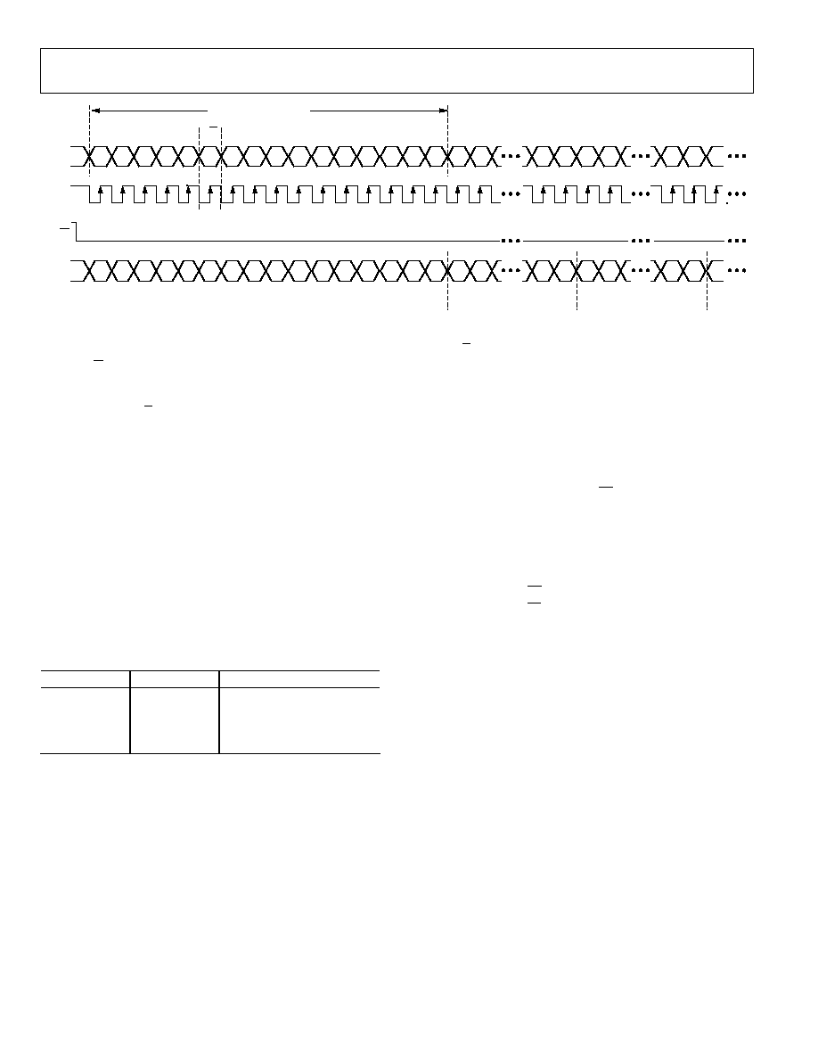
AD7142
Rev. 0 | Page 32 of 68
05702-
036
SDI
CW
15
CW
14
CW
13
CW
8
CW
1
CW
0
X
X
SCLK
CW
12
X
X
X
X
X
READBACK DATA FOR
STARTING REGISTER ADDRESS
X
X
1
32
2
3
4
15
16
17
18
31
34
33
48
47
49
CS
CW
11
CW
10
CW
9
CW
7
CW
2
CW
6
CW
5
CW
4
CW
3
11
12
13
14
5
6
7
8
9
10
XXX XXX XXX
XXX D15 D14
D1
D0
D1
D0
D15
D15
D14
XXX XXX XXX XXX XXX XXX XXX XXX XXX XXX XXX XXX
SDO
16-BIT COMMAND WORD
ENABLE WORD
R/W
REGISTER ADDRESS
NOTES
1. MULTIPLE REGISTERS CAN BE READ BACK CONTINUOUSLY.
2. THE 16-BIT CONTROL WORD MUST BE WRITTEN ON SDI: 5 BITS FOR ENABLE WORD, 1 BIT FOR R/W, AND 10 BITS FOR REGISTER ADDRESS.
3. THE ADDRESS AUTOMATICALLY INCREMENTS WITH EACH 16-BIT DATA-WORD BEING READ BACK ON THE SDO PIN.
4. CS IS HELD LOW UNTIL ALL REGISTER BITS HAVE BEEN READ BACK.
5. X DENOTES DON'T CARE.
6. XXX DENOTES HIGH IMPEDANCE THREE-STATE OUTPUT.
7. 16-BIT COMMAND WORD SETTINGS FOR SEQUENTIAL READBACK OPERATION:
CW[15:11] = 11100 (ENABLE WORD)
CW[10] = 1 (R/W)
CW[9:0] = [AD9, AD8, AD7, AD6, AD5, AD4, AD3, AD2, AD1, AD0] (STARTING MSB JUSTIFIED REGISTER ADDRESS)
READBACK DATA FOR
NEXT REGISTER ADDRESS
Figure 47. Sequential Register Readback SPI Timing
I
2
C COMPATIBLE INTERFACE
The AD7142-1 supports the industry standard 2-wire I
2
C serial
interface protocol. The two wires associated with the I
2
C timing are
the SCLK and the SDA inputs. The SDA is an I/O pin that allows
both register write and register readback operations. The AD7142-1
is always a slave device on the I
2
C serial interface bus.
It has a 7-bit device address, Address 0101 1XX. The lower two
bits are set by tying the ADD0 and ADD1 pins high or low. The
AD7142-1 responds when the master device sends its device
address over the bus. The AD7142-1 cannot initiate data
transfers on the bus.
Table 17. AD7142-1 I
2
C Device Address
ADD1 ADD0 I
2
C Address
0 0 0101
100
0 1 0101
101
1 0 0101
110
1 1 0101
111
Data Transfer
Data is transferred over the I
2
C serial interface in 8-bit bytes.
The master initiates a data transfer by establishing a start con-
dition, defined as a high-to-low transition on the serial data
line, SDA, while the serial clock line, SCLK, remains high. This
indicates that an address/data stream follows.
All slave peripherals connected to the serial bus respond to the
start condition and shift in the next eight bits, consisting of a
7-bit address (MSB first) plus an R/W bit that determines the
direction of the data transfer. The peripheral whose address
corresponds to the transmitted address responds by pulling the
data line low during the ninth clock pulse. This is known as the
acknowledge bit. All other devices on the bus now remain idle
while the selected device waits for data to be read from, or
written to it. If the R/W bit is a zero, the master writes to the
slave device. If the R/W bit is a one, the master reads from the
slave device.
Data is sent over the serial bus in a sequence of nine clock
pulses, eight bits of data followed by an acknowledge bit from
the slave device. Transitions on the data line must occur during
the low period of the clock signal and remain stable during the
high period, since a low-to-high transition when the clock is
high can be interpreted as a stop signal. The number of data
bytes transmitted over the serial bus in a single read or write
operation is limited only by what the master and slave devices
can handle.
When all data bytes are read or written, a stop condition is
established. A stop condition is defined by a low-to-high
transition on SDA while SCLK remains high. If the AD7142
encounters a stop condition, it returns to its idle condition, and
the address pointer register resets to Address 0x00.
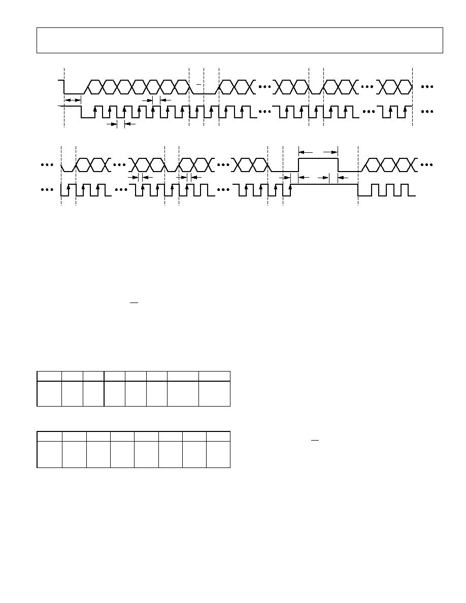
AD7142
Rev. 0 | Page 33 of 68
NOTES
1. A START CONDITION AT THE BEGINNING IS DEFINED AS A HIGH-TO-LOW TRANSITION ON SDA WHILE SCLK REMAINS HIGH.
2. A STOP CONDITION AT THE END IS DEFINED AS A LOW-TO-HIGH TRANSITION ON SDA WHILE SCLK REMAINS HIGH.
3. 7-BIT DEVICE ADDRESS [DEV A6:DEV A0] = [0 1 0 1 1 X X], WHERE X ARE DON'T CARE BITS.
4. 16-BIT REGISTER ADDRESS[A15:A0] = [X, X, X, X, X, X, A9, A8, A7, A6, A5, A4, A3, A2, A1, A0], WHERE X ARE DON'T CARE BITS.
5. REGISTER ADDRESS [A15:A8] AND REGISTER ADDRESS [A7:A0] ARE AWAYS SEPARATED BY A LOW ACK BIT.
6. REGISTER DATA [D15:D8] AND REGISTER DATA [D7:D0] ARE ALWAYS SEPARATED BY A LOW ACK BIT.
SDA
DEV
A6
DEV
A5
DEV
A4
R/W
A7
A6
SCLK
DEV
A3
A1
A0
1
26
2
3
4
17
18
19
20
25
DEV
A2
DEV
A1
DEV
A0
ACK
A15
A14
11
16
5
6
7
8
9
10
START
AD7142 DEVICE ADDRESS
A9
A8
REGISTER ADDRESS[A15:A8]
REGISTER ADDRESS[A7:A0]
ACK
D15
D14
D9
D8
35
27
28
29
34
37
36
43
38
44
D1
D0
D7
D6
REGISTER DATA[D15:D8]
REGISTER DATA[D7:D0]
ACK
ACK
45
46
ACK
STOP
DEV
A6
DEV
A5
DEV
A4
1
2
3
START
t
8
t
7
t
6
t
5
t
4
t
2
t
1
t
3
AD7142 DEVICE ADDRESS
057
02
-
0
37
Figure 48. Example of I
2
C Timing for Single Register Write Operation
Writing Data over the I
2
C Bus
The process for writing to the AD7142-1 over the I
2
C bus is
shown in Figure 48 and Figure 50. The device address is sent
over the bus followed by the R/W bit set to 0. This is followed
by two bytes of data that contain the 10-bit address of the
internal data register to be written. The following bit map shows
the upper register address bytes. Note that Bit 7 to Bit 2 in the
upper address byte are don't care bits. The address is contained
in the 10 LSBs of the register address bytes.
MSB
LSB
7 6 5 4 3 2 1
0
X X X X X X Register
Address
Bit 9
Register
Address
Bit 8
The following bit map shows the lower register address bytes.
MSB
LSB
7 6 5 4 3 2 1 0
Reg
Add
Reg
Add
Reg
Add
Reg
Add
Reg
Add
Reg
Add
Reg
Add
Reg
Add
Bit 7
Bit 6
Bit 5
Bit 4
Bit 3
Bit 2
Bit 1
Bit 0
The third data byte contains the 8 MSBs of the data to be
written to the internal register. The fourth data byte contains
the 8 LSBs of data to be written to the internal register.
The AD7142-1 address pointer register automatically increments
after each write. This allows the master to sequentially write to all
registers on the AD7142-1 in the same write transaction. However,
the address pointer register does not wrap around after the last
address.
Any data written to the AD7142-1 after the address pointer has
reached its maximum value is discarded.
All registers on the AD7142-1 are 16-bit. Two consecutive 8-bit
data bytes are combined and written to the 16-bit registers. To
avoid errors, all writes to the device must contain an even
number of data bytes.
To finish the transaction, the master generates a stop condition
on SDO, or generates a repeat start condition if the master is to
maintain control of the bus.
Reading Data over the I
2
C Bus
To read from the AD7142-1, the address pointer register must
first be set to the address of the required internal register. The
master performs a write transaction, and writes to the AD7142-1
to set the address pointer. The master then outputs a repeat start
condition to keep control of the bus, or if this is not possible, ends
the write transaction with a stop condition. A read transaction is
initiated, with the R/W bit set to 1.
The AD7142-1 supplies the upper eight bits of data from the
addressed register in the first readback byte, followed by the
lower eight bits in the next byte. This is shown in Figure 49 and
Figure 50.
Because the address pointer automatically increases after each
read, the AD7142-1 continues to output readback data until the
master puts a no acknowledge and stop condition on the bus. If
the address pointer reaches its maximum value, and the master
continues to read from the part, the AD7142-1 repeatedly sends
data from the last register addressed.
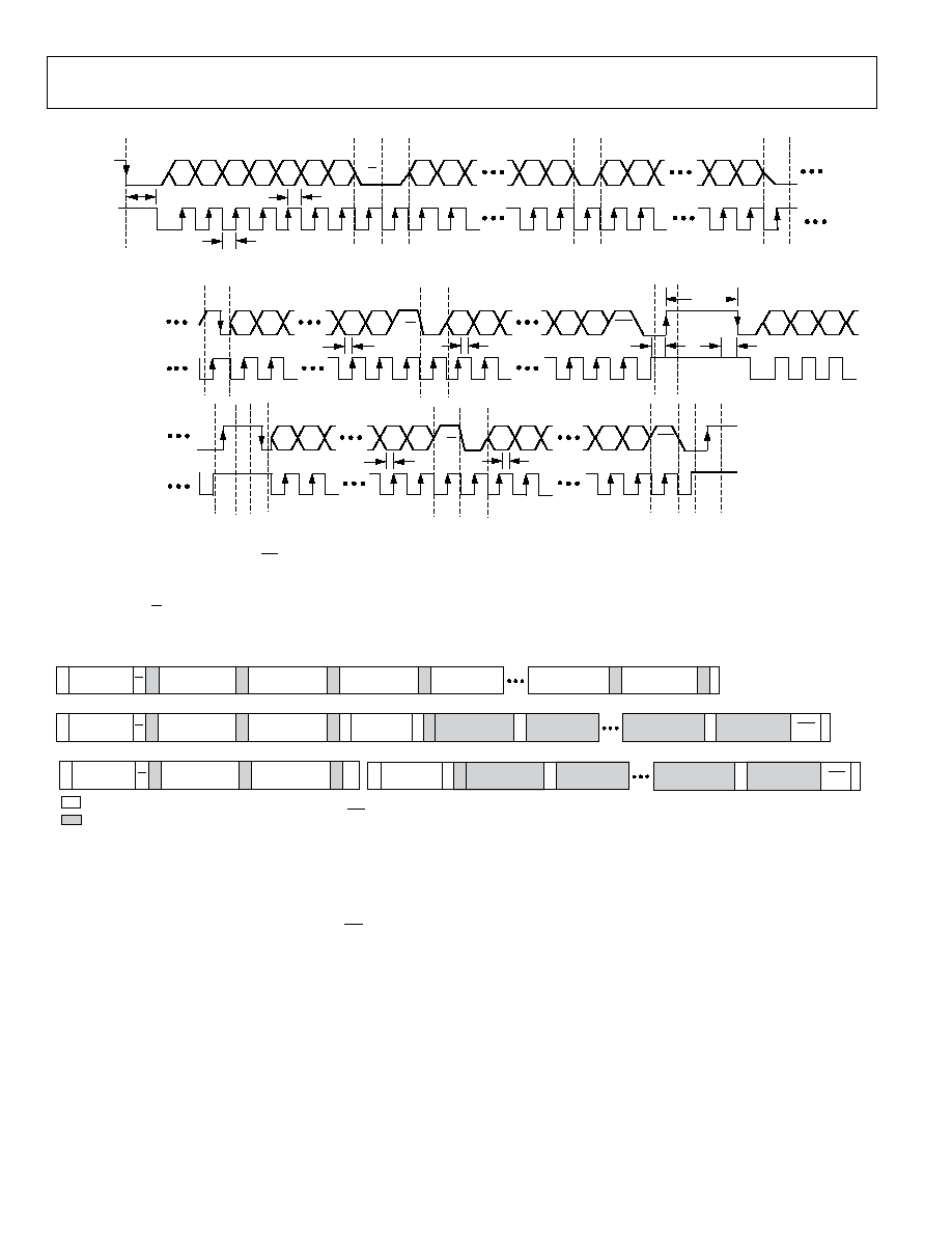
AD7142
Rev. 0 | Page 34 of 68
NOTES
1. A START CONDITION AT THE BEGINNING IS DEFINED AS A HIGH-TO-LOW TRANSITION ON SDA WHILE SCLK REMAINS HIGH.
2. A STOP CONDITION AT THE END IS DEFINED AS A LOW-TO-HIGH TRANSITION ON SDA WHILE SCLK REMAINS HIGH.
3. THE MASTER GENERATES THE ACK AT THE END OF THE READBACK TO SIGNAL THAT IT DOES NOT WANT ADDITIONAL DATA.
4. 7-BIT DEVICE ADDRESS [DEV A6:DEV A0] = [0 1 0 1 1 X X], WHERE THE TWO LSB X's ARE DON'T CARE BITS.
5. 16-BIT REGISTER ADDRESS[A15:A0] = [X, X, X, X, X, X, A9, A8, A7, A6, A5, A4, A3, A2, A1, A0], WHERE THE UPPER LSB X's ARE DON'T CARE BITS.
6. REGISTER ADDRESS [A15:A8] AND REGISTER ADDRESS [A7:A0] ARE ALWAYS SEPARATED BY A LOW ACK BITS.
7. REGISTER DATA [D15:D8] AND REGISTER DATA [D7:D0] ARE ALWAYS SEPARATED BY A LOW ACK BIT.
8. THE R/W BIT IS SET TO A1 TO INDICATE A READBACK OPERATION.
SDA
DEV
A6
DEV
A5
DEV
A4
R/W
A7
A6
SCLK
DEV
A3
A1
A0
1
26
2
3
4
17
18
19
20
25
DEV
A2
DEV
A1
DEV
A0
ACK
A15
A14
11
16
5
6
7
8
9
10
START
AD7142-1 DEVICE ADDRESS
A9
A8
REGISTER ADDRESS[A15:A8]
REGISTER ADDRESS[A7:A0]
ACK
35
28
30
34
37
36
44
38
45
D1
D0
D7
D6
REGISTER DATA[D7:D0]
SR
ACK
46
P
DEV
A6
DEV
A5
DEV
A4
1
2
3
t
8
t
7
t
6
t
5
t
4
t
2
t
1
t
3
AD7142 DEVICE ADDRESS
ACK
27
AD7142-1 DEVICE ADDRESS
DEV
A6
DEV
A5
DEV
A1
DEV
A0
057
02-
038
R/W
29
39
35
28
30
34
37
36
44
38
45
D1
D0
D7
D6
REGISTER DATA[D7:D0]
S
ACK
46
P
t
5
t
4
AD7142-1 DEVICE ADDRESS
DEV
A6
DEV
A5
DEV
A1
DEV
A0
R/W
29
39
P
USING
REPEATED START
SEPARATE READ AND
WRITE TRANSACTIONS
ACK
ACK
Figure 49. Example of I
2
C Timing for Single Register Readback Operation
AC
K
WRITE
OUTPUT FROM MASTER
OUTPUT FROM AD7142
S
P
P
AC
K
6-BIT DEVICE
ADDRESS
S = START BIT
P = STOP BIT
SR = REPEATED START BIT
ACK = ACKNOWLEDGE BIT
ACK = NO ACKNOWLEDGE BIT
REGISTER ADDR
[15:8]
REGISTER ADDR
[7:0]
WRITE DATA
HIGH BYTE [15:8]
WRITE DATA
LOW BYTE [7:0]
WRITE DATA
HIGH BYTE [15:8]
WRITE DATA
LOW BYTE [7:0]
AC
K
READ DATA
HIGH BYTE [15:8]
READ DATA
LOW BYTE [7:0]
AC
K
W
AC
K
AC
K
AC
K
AC
K
READ (USING REPEATED START)
S
AC
K
6-BIT DEVICE
ADDRESS
REGISTER ADDR
HIGH BYTE
REGISTER ADDR
LOW BYTE
6-BIT DEVICE
ADDRESS
READ DATA
HIGH BYTE [15:8]
AC
K
W
AC
K
AC
K
READ DATA
LOW BYTE [7:0]
057
02-
03
9
R
SR
P
AC
K
READ DATA
HIGH BYTE [15:8]
READ DATA
LOW BYTE [7:0]
AC
K
READ (WRITE TRANSACITON SETS UP REGISTER ADDRESS)
S
AC
K
6-BIT DEVICE
ADDRESS
REGISTER ADDR
HIGH BYTE
REGISTER ADDR
LOW BYTE
6-BIT DEVICE
ADDRESS
READ DATA
HIGH BYTE [15:8]
AC
K
W
AC
K
AC
K
READ DATA
LOW BYTE [7:0]
R
P
S
ACK
ACK
Figure 50. Example of Sequential I
2
C Write and Readback Operation
V
DRIVE
INPUT
The supply voltage to all pins associated with both the I
2
C and
SPI serial interfaces (SDO, SDI, SCLK, SDA, and CS) is separate
from the main V
CC
supplies and is connected to the V
DRIVE
pin.
This allows the AD7142 to be connected directly to processors
whose supply voltage is less than the minimum operating
voltage of the AD7142 without the need for external level-
shifters. The V
DRIVE
pin can be connected to voltage supplies as
low as 1.65 V and as high as DV
CC
.
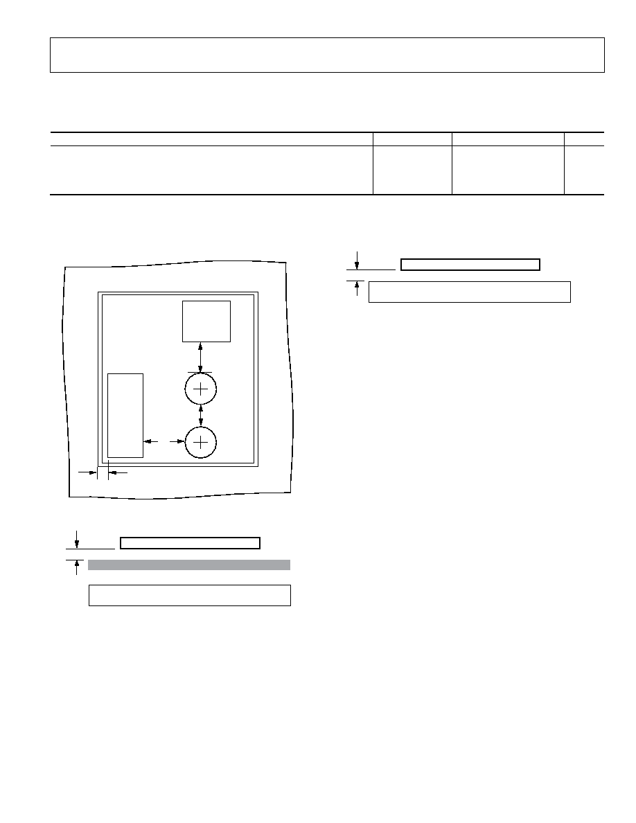
AD7142
Rev. 0 | Page 35 of 68
PCB DESIGN GUIDELINES
CAPACITIVE SENSOR BOARD MECHANICAL SPECIFICATIONS
Table 18.
Parameter
Symbol
Min
Typ
Max
Unit
Distance from Edge of Any Sensor to Edge of Metal Object
D
1
1.0
mm
Distance Between Sensor Edges
1
D
2
= D
3
= D
4
0 mm
Distance Between Bottom of Sensor Board and Controller Board or Metal
Casing
2
(4-Layer, 2-Layer, and Flex Circuit)
D
5
1.0
mm
1
The distance is dependent on the application and the positioning of the switches relative to each other and with respect to the user's finger positioning and handling.
Adjacent sensors, with 0 minimum space between them, are implemented differentially.
2
The 1.0 mm specification is meant to prevent direct sensor board contact with any conductive material. This specification does not guarantee no EMI coupling from
the controller board to the sensors. Address potential EMI coupling issues by placing a grounded metal shield between the capacitive sensor board and the main
controller board as shown in Figure 53.
05
70
2-
04
5
SLIDER
BUTTONS
CAPACITIVE SENSOR
PRINTED CIRCUIT
D
1
D
3
D
4
8-WAY
SWITCH
METAL OBJECT
D
2
Figure 51. Capacitive Sensor Board Mechanicals Top View
CAPACITIVE SENSOR BOARD
D
5
CONTROLLER PRINTED CIRCUIT BOARD OR METAL CASING
GROUNDED METAL SHIELD
057
02
-
04
6
Figure 52. Capacitive Sensor Board Mechanicals Side View
CAPACITIVE SENSOR BOARD
D
5
CONTROLLER PRINTED CIRCUIT BOARD OR METAL CASING
0
57
02
-
0
47
Figure 53. Capacitive Sensor Board with Grounded Shield
CHIP SCALE PACKAGES
The lands on the chip scale package (CP-32-3) are rectangular.
The printed circuit board pad for these should be 0.1 mm
longer than the package land length, and 0.05 mm wider than
the package land width. Center the land on the pad to maximize
the solder joint size.
The bottom of the chip scale package has a central thermal pad.
The thermal pad on the printed circuit board should be at least
as large as this exposed pad. To avoid shorting, provide a
clearance of at least 0.25 mm between the thermal pad and the
inner edges of the land pattern on the printed circuit board.
Thermal vias can be used on the printed circuit board thermal
pad to improve thermal performance of the package. If vias are
used, they should be incorporated in the thermal pad at a
1.2 mm pitch grid. The via diameter should be between 0.3 mm
and 0.33 mm, and the via barrel should be plated with 1 oz.
copper to plug the via.
Connect the printed circuit board thermal pad to GND.
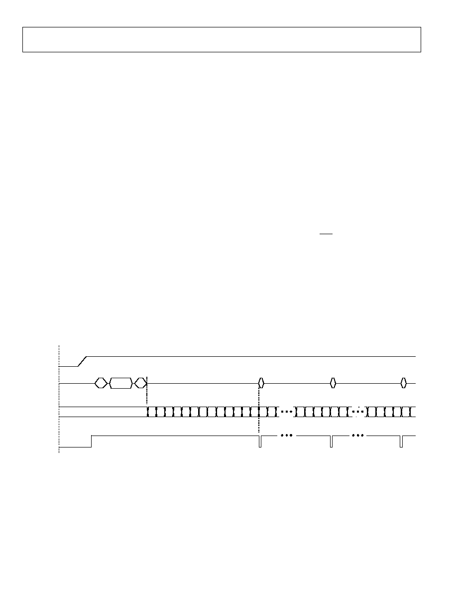
AD7142
Rev. 0 | Page 36 of 68
POWER-UP SEQUENCE
When the AD7142 is powered up, the following sequence is
recommended when initially developing the AD7142 and P
serial interface:
1.
Turn on the power supplies to the AD7142.
2.
Write to the Bank 2 registers at Address 0x080 through
Address 0x0DF. These registers are contiguous so a
sequential register write sequence can be applied.
Note: The Bank 2 register values are unique for each
application. Register values are provided by Analog
Devices after the sensor board has been developed.
3.
Write to the Bank 1 registers at Address 0x000 through
Address 0x007 as outlined below. These registers are
contiguous so a sequential register write sequence can be
applied (see Figure 45 and Figure 50).
Caution: At this time, Address 0x001 must remain set to
default value 0x0000 during this contiguous write
operation.
Register
values:
Address 0x000 = 0x00B2
Address 0x001 = 0x0000
Address 0x002 = 0x0690
Address 0x003 = 0x0664
Address 0x004 = 0x290F
Address 0x005 = 0x0000
Address 0x006 = 0x0000
Address 0x007 = 0x0001 (The AD7142 interrupt is asserted
approximately every 37 ms.)
4.
Write to the Bank 1 register, Address 0x001 = 0x0FFF.
5.
Read back the corresponding interrupt status register at
Address 0x008, Address 0x009, or Address 0x00A. This is
determined by the interrupt output configuration as
explained in the Interrupt Output section.
Note: The specific registers required to be readback depend
on each application. Analog Devices provides this
information after the sensor board has been developed.
6.
Repeat Step 5 every time INT is asserted.
05702-
040
FIRST CONVERSION SEQUENCE
CONVERSION
STAGE
0
CONVERSION STAGES DISABLED
1
2
3
4
5
6
7
8
9
10 11
0
1
2
9
10 11
0
1
2
9
10 11
0
1
SECOND CONVERSION
SEQUENCE
THIRD CONVERSION
SEQUENCE
Figure 54. Recommended Start-Up Sequence
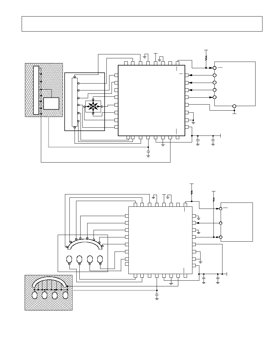
AD7142
Rev. 0 | Page 37 of 68
TYPICAL APPLICATION CIRCUITS
0
57
02
-
04
1
V
DRIVE
2.2k
8-WAY
SWITCH
HOST
WITH
SPI
INTERFACE
SS
SCK
MOSI
MISO
INT
V
HOST
SL
I
D
ER
AV
CC,
DV
CC
1.8V
AV
CC,
DV
CC
2.7V TO 3.6V
0.1µF
1µF TO 10µF
(OPTIONAL)
24
23
22
21
20
19
18
17
9
10
12
11
13
14
15
16
10nF
CIN3
CIN4
CIN5
CIN6
CIN7
CIN8
CIN9
CIN10
CI
N11
CI
N2
AV
CC
SR
C
AG
ND
CI
N12
CI
N13
C
SH
I
EL
D
SR
C
CS
IN
T
SDI
SCLK
V
DRIVE
DV
CC
DGND1
SDO
DGND2
V
RE
F
+
TE
S
T
GP
IO
CI
N0
CI
N1
V
RE
F
AD7142
32
31
30
29
28
27
26
25
1
2
3
4
5
6
7
8
S
E
NS
O
R
P
CB
L
A
Y
E
R
1
SE
N
SO
R
PC
B
L
A
Y
ER
2
Figure 55. Typical Application Circuit with SPI Interface
05702-
042
2.2k
SCK
SDO
INT
SEN
SO
R
PC
B
L
A
YER
1
CIN3
CIN4
CIN5
CIN6
CIN7
CIN8
CIN9
CIN10
CI
N2
CI
N1
1
AV
CC
SRC
AG
N
D
CI
N
1
2
CI
N
1
3
C
SH
I
EL
D
SR
C
ADD1
IN
T
ADD0
SCLK
VDRIVE
DV
CC
DGND1
SDA
DGND2
V
RE
F
+
T
EST
GP
IO
CI
N0
CI
N1
V
RE
F
AV
CC,
DV
CC
AV
CC,
DV
CC
2.7V TO 3.6V
0.1µF
1µF TO 10µF
(OPTIONAL)
AD7142-1
V
DRIVE
V
DRIVE
2.2k
SLIDER
1
2
3
4
5
6
7
8
24
23
22
21
20
19
18
17
9
10
11
12
13
14
15
16
32
31
30
29
28
27
26
25
10nF
BUTTONS
SE
N
SO
R
PC
B
L
A
YE
R
2
HOST
WITH
I
2
C
INTERFACE
Figure 56. Typical Application Circuit with I
2
C Interface
AD7142
Rev. 0 | Page 38 of 68
REGISTER MAP
The AD7142 address space is divided into three different
register banks, referred to as Bank 1, Bank 2, and Bank 3. Figure
57 illustrates the division of these three banks.
Bank 1 registers contain control registers, CDC conversion
control registers, interrupt enable registers, interrupt status
registers, CDC 16-bit conversion data registers, device ID
registers, and proximity status registers.
Bank 2 registers contain the configuration registers used for
uniquely configuring the CIN inputs for each conversion stage.
Initialize the Bank 2 configuration registers immediately after
power-up to obtain valid CDC conversion result data.
Bank 3 registers contain the results of each conversion stage.
These registers automatically update at the end of each conversion
sequence. Although these registers are primarily used by the
AD7142 internal data processing, they are accessible by the host
processor for additional external data processing, if desired.
Default values are undefined for Bank 2 registers and Bank 3
registers until after power up and configuration of the Bank 2
registers.
05
702
-
043
REGISTER BANK 1
ADDR 0x000
ADDR 0x018
ADDR 0x001
ADDR 0x005
ADDR 0x008
ADDR 0x00B
ADDR 0x017
ADDR 0x7F0
SET UP CONTROL
(1 REGISTER)
CALIBRATION AND SET UP
(4 REGISTERS)
INTERRUPT ENABLE
(3 REGISTERS)
INTERRUPT STATUS
(3 REGISTERS)
CDC 16-BIT CONVERSION DATA
(12 REGISTERS)
DEVICE ID REGISTER
INVALID DO NOT ACCESS
2
4
REG
I
ST
ER
S
REGISTER BANK 2
ADDR 0x080
ADDR 0x0B8
ADDR 0x088
ADDR 0x090
ADDR 0x098
ADDR 0x0A0
ADDR 0x0A8
ADDR 0x0B0
ADDR 0x0C8
ADDR 0x0C0
STAGE 0 CONFIGURATION
(8 REGISTERS)
STAGE 1 CONFIGURATION
(8 REGISTERS)
STAGE 2 CONFIGURATION
(8 REGISTERS)
STAGE 3 CONFIGURATION
(8 REGISTERS)
STAGE 4 CONFIGURATION
(8 REGISTERS)
STAGE 5 CONFIGURATION
(8 REGISTERS)
STAGE 6 CONFIGURATION
(8 REGISTERS)
STAGE 7 CONFIGURATION
(8 REGISTERS)
STAGE 8 CONFIGURATION
(8 REGISTERS)
STAGE 9 CONFIGURATION
(8 REGISTERS)
STAGE 10 CONFIGURATION
(8 REGISTERS)
STAGE 11 CONFIGURATION
(8 REGISTERS)
ADDR 0x0D8
ADDR 0x0D0
9
6
R
EG
I
ST
ER
S
REGISTER BANK 3
ADDR 0x0E0
ADDR 0x0B8
ADDR 0x088
ADDR 0x090
ADDR 0x098
ADDR 0x0A0
ADDR 0x0A8
ADDR 0x0B0
ADDR 0x0C8
ADDR 0x0C0
STAGE 0 RESULTS
(36 REGISTERS)
ADDR 0x28F
ADDR 0x0D0
43
2 RE
G
I
S
T
E
R
S
STAGE 1 RESULTS
(36 REGISTERS)
STAGE 10 RESULTS
(36 REGISTERS)
STAGE 9 RESULTS
(36 REGISTERS)
STAGE 8 RESULTS
(36 REGISTERS)
STAGE 7 RESULTS
(36 REGISTERS)
STAGE 6 RESULTS
(36 REGISTERS)
STAGE 5 RESULTS
(36 REGISTERS)
STAGE 4 RESULTS
(36 REGISTERS)
STAGE 3 RESULTS
(36 REGISTERS)
STAGE 2 RESULTS
(36 REGISTERS)
STAGE 11 RESULTS
(36 REGISTERS)
PROXIMITY STATUS REGISTER
ADDR 0x042
INVALID DO NOT ACCESS
ADDR 0x043
Figure 57. Layout of Bank 1 Registers, Bank 2 Registers, and Bank 3 Registers
AD7142
Rev. 0 | Page 39 of 68
DETAILED REGISTER DESCRIPTIONS
BANK 1 REGISTERS
All addresses and default values are expressed in hexadecimal.
Table 19. PWR_CONTROL Register
Address Data Bit
Default
Value
Type
Name
Description
0x000
[1:0]
0
R/W
POWER_MODE
Operating modes
00 = full power mode (normal operation, CDC
conversions approximately every 36 ms)
01 = full shutdown mode (no CDC conversions)
10 = low power mode (automatic wake up operation)
11 = full shutdown mode (no CDC conversions)
[3:2]
0
LP_CONV_DELAY
Low power mode conversion delay
00 = 200 ms
01 = 400 ms
10 = 600 ms
11 = 800 ms
[7:4]
0
SEQUENCE_STAGE_NUM
Number of stages in sequence (N + 1)
0000 = 1 conversion stage in sequence
0001 = 2 conversion stages in sequence
......
Maximum value = 1011 = 12 conversion stages per
sequence
[9:8]
0
DECIMATION
ADC decimation factor
00 = decimate by 256
01 = decimate by 128
10 = do not use this setting
11 = do not use this setting
[10]
0
SW_RESET
Software reset control (self-clearing)
1 = resets all registers to default values
[11]
0
INT_POL
Interrupt polarity control
0 = active low
1 = active high
[12]
0
EXCITATION_SOURCE
Excitation source control for Pin 15
0 = enable output
1 = disable output
[13]
0
SRC
Excitation source control for Pin 16
0 = enable output
1 = disable output
[15:14]
0
CDC_BIAS
CDC bias current control
00 = normal operation
01 = normal operation + 20%
10 = normal operation + 35%
11 = normal operation + 50%
AD7142
Rev. 0 | Page 40 of 68
Table 20. STAGE_CAL_EN Register
Address
Data Bit
Default
Value
Type
Name
Description
0x001
[0]
0
R/W
STAGE0_CAL_EN
STAGE0 calibration enable
0 = disable
1 = enable
[1]
0
STAGE1_CAL_EN
STAGE1 calibration enable
0 = disable
1 = enable
[2]
0
STAGE2_CAL_EN
STAGE2 calibration enable
0 = disable
1 = enable
[3]
0
STAGE3_CAL_EN
STAGE3 calibration enable
0 = disable
1 = enable
[4]
0
STAGE4_CAL_EN
STAGE4 calibration enable
0 = disable
1 = enable
[5]
0
STAGE5_CAL_EN
STAGE5 calibration enable
0 = disable
1 = enable
[6]
0
STAGE6_CAL_EN
STAGE6 calibration enable
0 = disable
1 = enable
[7]
0
STAGE7_CAL_EN
STAGE7 calibration enable
0 = disable
1 = enable
[8]
0
STAGE8_CAL_EN
STAGE8 calibration enable
0 = disable
1 = enable
[9]
0
STAGE9_CAL_EN
STAGE9 calibration enable
0 = disable
1 = enable
[10]
0
STAGE10_CAL_EN
STAGE10 calibration enable
0 = disable
1 = enable
[11]
0
STAGE11_CAL_EN
STAGE11 calibration enable
0 = disable
1 = enable
[13:12]
0
AVG_FP_SKIP
Full power mode skip control
00 = skip 3 samples
01 = skip 7 samples
10 = skip 15 samples
11 = skip 31 samples
[15:14]
0
AVG_LP_SKIP
Low power mode skip control
00 = use all samples
01 = skip 1 sample
10 = skip 2 samples
11 = skip 3 samples
AD7142
Rev. 0 | Page 41 of 68
Table 21. AMB_COMP_CTRL0 Register
Address
Data Bit
Default
Value
Type
Name
Description
0x002
[3:0]
0
R/W
FF_SKIP_CNT
Fast filter skip control (N+1)
0000 = no sequence of results are skipped
0001 = one sequence of results is skipped for every
one allowed into Fast FIFO
0010 = two sequences of results are skipped for every
one allowed into Fast FIFO
1011 = maximum value = 12 sequences of results are
skipped for every one allowed into Fast FIFO
[7:4]
F
FP_PROXIMITY_CNT
Full power mode proximity period
[11:8]
F
LP_PROXIMITY_CNT
Low power mode proximity period
[13:12]
0
PWR_DOWN_TIMEOUT
Full power to low power mode time out control
00 = 1.25 × (FP_PROXIMITY_CNT)
01 = 1.50 × (FP_PROXIMITY_CNT)
10 = 1.75 × (FP_PROXIMITY_CNT)
11 = 2.00 × (FP_PROXIMITY_CNT)
[14]
0
FORCED_CAL
Forced calibration control
0 = normal operation
1 = forces all conversion stages to recalibrate
[15]
0
CONV_RESET
Conversion reset control (self-clearing)
0 = normal operation
1 = resets the conversion sequence back to STAGE0.
Table 22. AMB_COMP_CTRL1 Register
Address
Data Bit
Default
Value
Type
Name
Description
0x003
[7:0]
64
R/W
PROXIMITY_RECAL_LVL
Proximity recalibration level
[13:8]
1
PROXIMITY_DETECTION_RATE
Proximity detection rate
[15:14]
0
SLOW_FILTER_UPDATE_LVL
Slow filter update level
Table 23. AMB_COMP_CTRL2 Register
Address
Data Bit
Default
Value
Type
Name
Description
0x004
[9:0]
3FF
R/W
FP_PROXIMITY_RECAL
Full power mode proximity recalibration time control
[15:10]
3F
LP_PROXIMITY_RECAL
Low power mode proximity recalibration time control
Table 24. STAGE_LOW_INT_EN Register
Address Data Bit
Default
Value
Type
Name
Description
0x005
[0]
0
R/W
STAGE0_LOW_INT_EN
STAGE0 low interrupt enable
0 = interrupt source disabled
1 = INT asserted if STAGE0 low threshold is exceeded
[1]
0
STAGE1_LOW_INT_EN
STAGE1 low interrupt enable
0 = interrupt source disabled
1 = INT asserted if STAGE0 low threshold is exceeded
[2]
0
STAGE2_LOW_INT_EN
STAGE2 low interrupt enable
0 = interrupt source disabled
1 = INT asserted if STAGE0 low threshold is exceeded
[3]
0
STAGE3_LOW_INT_EN
STAGE3 low interrupt enable
0 = interrupt source disabled
1 = INT asserted if STAGE0 low threshold is exceeded
AD7142
Rev. 0 | Page 42 of 68
Address Data Bit
Default
Value
Type
Name
Description
[4]
0
STAGE4_LOW_INT_EN
STAGE4 low interrupt enable
0 = interrupt source disabled
1 = INT asserted if STAGE0 low threshold is exceeded
[5]
0
STAGE5_LOW_INT_EN
STAGE5 low interrupt enable
0 = interrupt source disabled
1 = INT asserted if STAGE0 low threshold is exceeded
[6]
0
STAGE6_LOW_INT_EN
STAGE6 low interrupt enable
0 = interrupt source disabled
1 = INT asserted if STAGE0 low threshold is exceeded
[7]
0
STAGE7_LOW_INT_EN
STAGE7 low interrupt enable
0 = interrupt source disabled
1 = INT asserted if STAGE0 low threshold is exceeded
[8]
0
STAGE8_LOW_INT_EN
STAGE8 low interrupt enable
0 = interrupt source disabled
1 = INT asserted if STAGE0 low threshold is exceeded
[9]
0
STAGE9_LOW_INT_EN
STAGE9 low interrupt enable
0 = interrupt source disabled
1 = INT asserted if STAGE0 low threshold is exceeded
[10]
0
STAGE10_LOW_INT_EN
STAGE10 low interrupt enable
0 = interrupt source disabled
1 = INT asserted if STAGE0 low threshold is exceeded
[11]
0
STAGE11_LOW_INT_EN
STAGE11 low interrupt enable
0 = interrupt source disabled
1 = INT asserted if STAGE0 low threshold is exceeded
[13:12]
0
GPIO_SETUP
GPIO setup
00 = disable GPIO pin
01 = configure GPIO as an input
10 = configure GPIO as an active low output
11 = configure GPIO as an active high output
[15:14]
0
GPIO_INPUT_CONFIG
GPIO input configuration
00 = triggered on negative level
01 = triggered on positive edge
10 = triggered on negative edge
11 = triggered on positive level
Table 25. STAGE_HIGH_INT_EN Register
Address Data Bit
Default
Value
Type
Name
Description
0x006
[0]
0
R/W
STAGE0_HIGH_INT_EN
STAGE0 high interrupt enable
0 = interrupt source disabled
1 = INT asserted if STAGE0 high threshold is exceeded
[1]
0
STAGE1_HIGH_INT_EN
STAGE1 high interrupt enable
0 = interrupt source disabled
1 = INT asserted if STAGE0 high threshold is exceeded
[2]
0
STAGE2_HIGH_INT_EN
STAGE2 high interrupt enable
0 = interrupt source disabled
1 = INT asserted if STAGE0 high threshold is exceeded
[3]
0
STAGE3_HIGH_INT_EN
STAGE3 high interrupt enable
0 = interrupt source disabled
1 = INT asserted if STAGE0 high threshold is exceeded
AD7142
Rev. 0 | Page 43 of 68
Address Data Bit
Default
Value
Type
Name
Description
[4]
0
STAGE4_HIGH_INT_EN
STAGE4 high interrupt enable
0 = interrupt source disabled
1 = INT asserted if STAGE0 high threshold is exceeded
[5]
0
STAGE5_HIGH_INT_EN
STAGE5 high interrupt enable
0 = interrupt source disabled
1 = INT asserted if STAGE0 high threshold is exceeded
[6]
0
STAGE6_HIGH_INT_EN
STAGE6 high interrupt enable
0 = interrupt source disabled
1 = INT asserted if STAGE0 high threshold is exceeded
[7]
0
STAGE7_HIGH_INT_EN
STAGE7 high interrupt enable
0 = interrupt source disabled
1 = INT asserted if STAGE0 high threshold is exceeded
[8]
0
STAGE8_HIGH_INT_EN
STAGE8 high interrupt enable
0 = interrupt source disabled
1 = INT asserted if STAGE0 high threshold is exceeded
[9]
0
STAGE9_HIGH_INT_EN
STAGE9 sensor interrupt low limit control
0 = interrupt source disabled
1 = INT asserted if STAGE10_LOW is exceeded
[10]
0
STAGE10_HIGH_INT_EN
STAGE10 high interrupt enable
0 = interrupt source disabled
1 = INT asserted if STAGE0 high threshold is exceeded
[11]
0
STAGE11_HIGH_INT_EN
STAGE11 high interrupt enable
0 = interrupt source disabled
1 = INT asserted if STAGE0 high threshold is exceeded
[15:12]
Unused
Set unused register bits = 0
Table 26. STAGE_COMPLETE_INT_EN Register
Address Data Bit
Default
Value
Type
Name
Description
0x007
[0]
0
R/W
STAGE0_COMPLETE_EN
STAGE0 conversion interrupt control
0 = interrupt source disabled
1 = INT asserted at completion of STAGE0 conversion
[1]
0
STAGE1_COMPLETE_EN
STAGE1 conversion interrupt control
0 = interrupt source disabled
1 = INT asserted at completion of STAGE1 conversion
[2]
0
STAGE2_COMPLETE_EN
STAGE2 conversion interrupt control
0 = interrupt source disabled
1 = INT asserted at completion of STAGE2 conversion
[3]
0
STAGE3_COMPLETE_EN
STAGE3 conversion interrupt control
0 = interrupt source disabled
1 = INT asserted at completion of STAGE3 conversion
[4]
0
STAGE4_COMPLETE_EN
STAGE4 conversion interrupt control
0 = interrupt source disabled
1 = INT asserted at completion of STAGE4 conversion
[5]
0
STAGE5_COMPLETE_EN
STAGE5 conversion interrupt control
0 = interrupt source disabled
1 = INT asserted at completion of STAGE5 conversion
[6]
0
STAGE6_COMPLETE_EN
STAGE6 conversion interrupt control
0 = interrupt source disabled
1 = INT asserted at completion of STAGE6 conversion
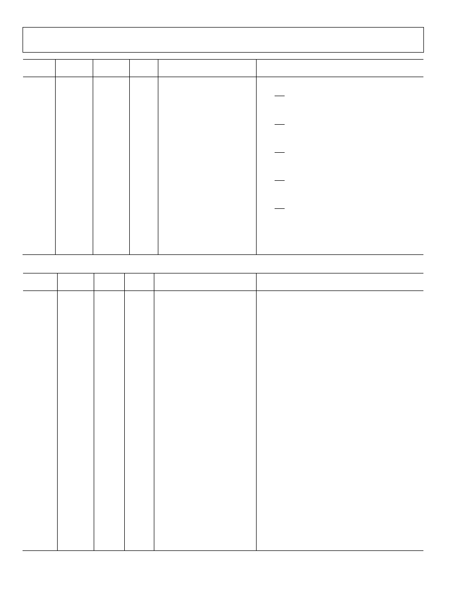
AD7142
Rev. 0 | Page 44 of 68
Address Data Bit
Default
Value
Type
Name
Description
[7]
0
STAGE7_COMPLETE_EN
STAGE7 conversion interrupt control
0 = interrupt source disabled
1 = INT asserted at completion of STAGE7 conversion
[8]
0
STAGE8_COMPLETE_EN
STAGE8 conversion complete interrupt control
0 = interrupt source disabled
1 = INT asserted at completion of STAGE8 conversion
[9]
0
STAGE9_COMPLETE_EN
STAGE9 conversion interrupt control
0 = interrupt source disabled
1 = INT asserted at completion of STAGE9 conversion
[10]
0
STAGE10_COMPLETE_EN
STAGE10 conversion interrupt control
0 = interrupt source disabled
1 = INT asserted at completion of STAGE10 conversion
[11]
0
STAGE11_COMPLETE_EN
STAGE11 conversion interrupt control
0 = interrupt source disabled
1 = INT asserted at completion of STAGE11 conversion
[12]
0
GPIO_INT_EN
Interrupt control when GPIO input pin changes level
0 = disabled
1 = enabled
[15:13]
Unused
Set unused register bits = 0
Table 27. STAGE_LOW_LIMIT_INT Register
1
Address
Data Bit
Default
Value
Type
Name
Description
0x008
[0]
0
R
STAGE0_LOW_LIMIT_INT
STAGE0 CDC conversion low limit interrupt result
1 = indicates STAGE0_LOW_THRESHOLD value was
exceeded
[1]
0
STAGE1_LOW_LIMIT_INT
STAGE1 CDC conversion low limit interrupt result
1 = indicates STAGE1_LOW_THRESHOLD value was
exceeded
[2]
0
STAGE2_LOW_LIMIT_INT
STAGE2 CDC conversion low limit interrupt result
1 = indicates STAGE2_LOW_THRESHOLD value was
exceeded
[3]
0
STAGE3_LOW_LIMIT_INT
STAGE3 CDC conversion low limit interrupt result
1 = indicates STAGE3_LOW_THRESHOLD value was
exceeded
[4]
0
STAGE4_LOW_LIMIT_INT
STAGE4 CDC conversion low limit interrupt result
1 = indicates STAGE4_LOW_THRESHOLD value was
exceeded
[5]
0
STAGE5_LOW_LIMIT_INT
STAGE5 CDC conversion low limit interrupt result
1 = indicates STAGE5_LOW_THRESHOLD value was
exceeded
[6]
0
STAGE6_LOW_LIMIT_INT
STAGE6 CDC conversion low limit interrupt result
1 = indicates STAGE6_LOW_THRESHOLD value was
exceeded
[7]
0
STAGE7_LOW_LIMIT_INT
STAGE7 CDC conversion low limit interrupt result
1 = indicates STAGE7_LOW_THRESHOLD value was
exceeded
[8]
0
STAGE8_LOW_LIMIT_INT
STAGE8 CDC conversion low limit interrupt result
1 = indicates STAGE8_LOW_THRESHOLD value was
exceeded
[9]
0
STAGE9_LOW_LIMIT_INT
STAGE9 CDC conversion low limit interrupt result
1 = indicates STAGE9_LOW_THRESHOLD value was
exceeded
AD7142
Rev. 0 | Page 45 of 68
Address
Data Bit
Default
Value
Type
Name
Description
[10]
0
STAGE10_LOW_LIMIT_INT
STAGE10 CDC Conversion Low Limit Interrupt result
1 = indicates STAGE10_LOW_THRESHOLD value was
exceeded
[11]
0
STAGE11_LOW_LIMIT_INT
STAGE11 CDC conversion low limit interrupt result
1 = indicates STAGE11_LOW_THRESHOLD value was
exceeded
[15:12]
Unused
Set unused register bits = 0
1
Registers self-clear to 0 after readback, provided that the limits are not exceeded.
Table 28. STAGE_HIGH_LIMIT_INT Register
1
Address
Data Bit
Default
Value
Type
Name
Description
0x009
[0]
0
R
STAGE0_HIGH_LIMIT_INT
STAGE0 CDC conversion high limit interrupt result
1 = indicates STAGE0_HIGH_THRESHOLD value was
exceeded
[1]
0
STAGE1_HIGH_LIMIT_INT
STAGE1 CDC conversion high limit interrupt result
1 = indicates STAGE1_HIGH_THRESHOLD value was
exceeded
[2]
0
STAGE2_HIGH_LIMIT_INT
Stage2 CDC conversion high limit interrupt result
1 = indicates STAGE2_HIGH_THRESHOLD value was
exceeded
[3]
0
STAGE3_HIGH_LIMIT_INT
STAGE3 CDC conversion high limit interrupt result
1 = indicates STAGE3_HIGH_THRESHOLD value was
exceeded
[4]
0
STAGE4_HIGH_LIMIT_INT
STAGE4 CDC conversion high limit interrupt result
1 = indicates STAGE4_HIGH_THRESHOLD value was
exceeded
[5]
0
STAGE5_HIGH_LIMIT_INT
STAGE5 CDC conversion high limit interrupt result
1 = indicates STAGE5_HIGH_THRESHOLD value was
exceeded
[6]
0
STAGE6_HIGH_LIMIT_INT
STAGE6 CDC conversion high limit interrupt result
1 = indicates STAGE6_HIGH_THRESHOLD value was
exceeded
[7]
0
STAGE7_HIGH_LIMIT_INT
STAGE7 CDC conversion high limit interrupt result
1 = indicates STAGE7_HIGH_THRESHOLD value was
exceeded
[8]
0
STAGE8_HIGH_LIMIT_INT
STAGE8 CDC conversion high limit interrupt result
1 = indicates STAGE8_HIGH_THRESHOLD value was
exceeded
[9]
0
STAGE9_HIGH_LIMIT_INT
STAGE9 CDC conversion high limit interrupt result
1 = indicates STAGE9_HIGH_THRESHOLD value was
exceeded
[10]
0
STAGE10_HIGH_LIMIT_INT
STAGE10
CDC conversion high limit interrupt result
1 = indicates STAGE10_HIGH_THRESHOLD value was
exceeded
[11]
0
STAGE11_HIGH_LIMIT_INT
STAGE11
CDC conversion high limit interrupt result
1 = indicates STAGE11_HIGH_THRESHOLD value was
exceeded
[15:12]
Unused
Set unused register bits = 0
1
Registers self-clear to 0 after readback, provided that the limits are not exceeded.

AD7142
Rev. 0 | Page 46 of 68
Table 29. STAGE_COMPLETE_LIMIT_INT Register
7
Address
Data Bit
Default
Value
Type
Name
Description
0x00A
[0]
0
R
STAGE0_COMPLETE_STATUS_INT
STAGE0 conversion complete register interrupt status
1 = indicates STAGE0 conversion completed
[1]
0
STAGE1_COMPLETE_STATUS_INT
STAGE1 conversion complete register interrupt status
1 = indicates STAGE0 conversion completed
[2]
0
STAGE2_COMPLETE_STATUS_INT
STAGE2 conversion complete register interrupt status
1 = indicates STAGE0 conversion completed
[3]
0
STAGE3_COMPLETE_STATUS_INT
STAGE3 conversion complete register interrupt status
1 = indicates STAGE0 conversion completed
[4]
0
STAGE4_COMPLETE_STATUS_INT
STAGE4 conversion complete register interrupt status
1 = indicates STAGE0 conversion completed
[5]
0
STAGE5_COMPLETE_STATUS_INT
STAGE5 conversion complete register interrupt status
1 = indicates STAGE0 conversion completed
[6]
0
STAGE6_COMPLETE_STATUS_INT
STAGE6 conversion complete register interrupt status
1 = indicates STAGE0 conversion completed
[7]
0
STAGE7_COMPLETE_STATUS_INT
STAGE7 conversion complete register interrupt status
1 = indicates STAGE0 conversion completed
[8]
0
STAGE8_COMPLETE_STATUS_INT
STAGE8 conversion complete register interrupt status
1 = indicates STAGE0 conversion completed
[9]
0
STAGE9_COMPLETE_STATUS_INT
STAGE9 conversion complete register interrupt status
1 = indicates STAGE0 conversion completed
[10]
0
STAGE10_COMPLETE_STATUS_INT
STAGE10 conversion complete register interrupt status
1 = indicates STAGE0 conversion completed
[11]
0
STAGE11_COMPLETE_STATUS_INT
STAGE11 conversion complete register interrupt status
1 = indicates STAGE0 conversion completed
[12]
0
GPIO_STATUS
GPIO input pin status
1 = indicates level on GPIO pin has changed
[15:13]
Unused
Set unused register bits = 0
7
Registers self-clear to 0 after readback, provided that the limits are not exceeded.
Table 30. CDC 16-Bit Conversion Data Registers
Address Data Bit
Default
Value
Type
Name
Description
0x00B
[15:0]
0
R
ADC_RESULT_S0
STAGE0 CDC 16-bit conversion data
0x00C
[15:0]
0
R
ADC_RESULT_S1
STAGE1 CDC 16-bit conversion data
0x00D
[15:0]
0
R
ADC_RESULT_S2
STAGE2 CDC 16-bit conversion data
0x00E
[15:0]
0
R
ADC_RESULT_S3
STAGE3 CDC 16-bit conversion data
0x00F
[15:0]
0
R
ADC_RESULT_S4
STAGE4 CDC 16-bit conversion data
0x010
[15:0]
0
R
ADC_RESULT_S5
STAGE5 CDC 16-bit conversion data
0x011
[15:0]
0
R
ADC_RESULT_S6
STAGE6 CDC 16-bit conversion data
0x012
[15:0]
0
R
ADC_RESULT_S7
STAGE7 CDC 16-bit conversion data
0x013
[15:0]
0
R
ADC_RESULT_S8
STAGE8 CDC 16-bit conversion data
0x014
[15:0]
0
R
ADC_RESULT_S9
STAGE9 CDC 16-bit conversion data
0x015
[15:0]
0
R
ADC_RESULT_S10
STAGE10 CDC 16-bit conversion data
0x016
[15:0]
0
R
ADC_RESULT_S11
STAGE11 CDC 16-bit conversion data
AD7142
Rev. 0 | Page 47 of 68
Table 31. Device ID Register
Address Data Bit
Default
Value
Type
Name
Description
0x017
[3:0]
3
R
REVISION_CODE
AD7142 revision code
[15:4]
E62
DEVID
AD7142 device ID = 110110100010
Table 32. Proximity Status Register
Address Data Bit
Default
Value
Type
Name
Description
0x042
[0]
0
R
STAGE0_PROXIMITY_STATUS
STAGE0 proximity status register
1 = indicates proximity has been detected on STAGE0
[1]
0
R
STAGE1_PROXIMITY_STATUS
STAGE1 proximity status register
1 = indicates proximity has been detected on STAGE1
[2]
0
R
STAGE2_PROXIMITY_STATUS
STAGE2 proximity status register
1 = indicates proximity has been detected on STAGE2
[3]
0
R
STAGE3_PROXIMITY_STATUS
STAGE3 proximity status register
1 = indicates proximity has been detected on STAGE3
[4]
0
R
STAGE4_PROXIMITY_STATUS
STAGE4 proximity status register
1 = indicates proximity has been detected on STAGE4
[5]
0
R
STAGE5_PROXIMITY_STATUS
STAGE5 proximity status register
1 = indicates proximity has been detected on STAGE5
[6]
0
R
STAGE6_PROXIMITY_STATUS
STAGE6 proximity status register
1 = indicates proximity has been detected on STAGE6
[7]
0
R
STAGE7_PROXIMITY_STATUS
STAGE7 proximity status register
1 = indicates proximity has been detected on STAGE7
[8]
0
R
STAGE8_PROXIMITY_STATUS
STAGE8 proximity status register
1 = indicates proximity has been detected on STAGE8
[9]
0
R
STAGE9_PROXIMITY_STATUS
STAGE9 proximity status register
1 = indicates proximity has been detected on STAGE9
[10]
0
R
STAGE10_PROXIMITY_STATUS
STAGE10 proximity status register
1 = indicates proximity has been detected on STAGE10
[11]
0
R
STAGE11_PROXIMITY_STATUS
STAGE11 proximity status register
1 = indicates proximity has been detected on STAGE11
[15:0]
Unused
Set unused register bits = 0
AD7142
Rev. 0 | Page 48 of 68
BANK 2 REGISTERS
All address values are expressed in hexadecimal.
Table 33. STAGE0 Configuration Registers
Address
Data Bit
Default
Value
Type
Name
Description
0x080 [15:0] X
R/W
STAGE0_CONNECTION[6:0]
STAGE0 CIN(6:0) connection setup (see Table 45)
0x081 [15:0] X
R/W
STAGE0_CONNECTION[13:7]
STAGE0 CIN(13:7) connection setup (see Table 46)
0x082
[15:0]
X
R/W
STAGE0_AFE_OFFSET
STAGE0 AFE offset control (see Table 47)
0x083
[15:0]
X
R/W
STAGE0_SENSITIVITY
STAGE0 sensitivity control (see Table 48)
0x084
[15:0]
X
R/W
STAGE0_OFFSET_LOW
STAGE0 initial offset low value
0x085
[15:0]
X
R/W
STAGE0_OFFSET_HIGH
STAGE0 initial offset high value
0x086
[15:0]
X
R/W
STAGE0_OFFSET_HIGH_CLAMP
STAGE0 offset high clamp value
0x087
[15:0]
X
R/W
STAGE0_ OFFSET_LOW_CLAMP
STAGE0 offset low clamp value
Table 34. STAGE1 Configuration Registers
Address
Data
Bit
Default
Value
Type
Name
Description
0x088 [15:0]
X
R/W STAGE1_CONNECTION[6:0]
STAGE1 CIN(6:0) connection setup (see Table 45)
0x089 [15:0]
X
R/W STAGE1_CONNECTION[13:7]
STAGE1 CIN(13:7) connection setup (see Table 46)
0x08A
[15:0]
X
R/W
STAGE1_AFE_OFFSET
STAGE1 AFE offset control (see Table 47)
0x08B
[15:0]
X
R/W
STAGE1_SENSITIVITY
STAGE1 sensitivity control (see Table 48)
0x08C
[15:0]
X
R/W
STAGE1_OFFSET_LOW
STAGE1 initial offset low value
0x08D
[15:0]
X
R/W
STAGE1_OFFSET_HIGH
STAGE1 initial offset high value
0x08E
[15:0]
X
R/W
STAGE1_OFFSET_HIGH_CLAMP
STAGE1 offset high clamp value
0x08F
[15:0]
X
R/W
STAGE1_OFFSET_LOW_CLAMP
STAGE1 offset low clamp value
Table 35. STAGE2 Configuration Registers
Address
Data
Bit
Default
Value
Type
Name
Description
0x090 [15:0]
X
R/W STAGE2_CONNECTION[6:0]
STAGE2 CIN(6:0) connection setup (see Table 45)
0x091 [15:0]
X
R/W STAGE2_CONNECTION[13:7]
STAGE2 CIN(13:7) connection setup (see Table 46)
0x092
[15:0]
X
R/W
STAGE2_AFE_OFFSET
STAGE2 AFE offset control (see Table 47)
0x093
[15:0]
X
R/W
STAGE2_SENSITIVITY
STAGE2 sensitivity control (see Table 48)
0x094
[15:0]
X
R/W
STAGE2_OFFSET_LOW
STAGE2 initial offset low value
0x095
[15:0]
X
R/W
STAGE2_OFFSET_HIGH
STAGE2 initial offset high value
0x096
[15:0]
X
R/W
STAGE2_OFFSET_HIGH_CLAMP
STAGE2 offset high clamp value
0x097
[15:0]
X
R/W
STAGE2_OFFSET_LOW_CLAMP
STAGE2 offset low clamp value
AD7142
Rev. 0 | Page 49 of 68
Table 36. STAGE3 Configuration Registers
Address Data Bit
Default
Value
Type
Name
Description
0x098 [15:0]
X
R/W STAGE3_CONNECTION[6:0]
STAGE3 CIN(6:0) connection setup (see Table 45
)
0x099 [15:0]
X
R/W STAGE3_CONNECTION[13:7]
STAGE3 CIN(13:7) connection setup (see Table 46)
0x09A
[15:0]
X
R/W
STAGE3_AFE_OFFSET
STAGE3 AFE offset control (see Table 47)
0x09B
[15:0]
X
R/W
STAGE3_SENSITIVITY
STAGE3 sensitivity control (see Table 48)
0x09C
[15:0]
X
R/W
STAGE3_OFFSET_LOW
STAGE3 initial offset low value
0x09D
[15:0]
X
R/W
STAGE3_OFFSET_HIGH
STAGE3 initial offset high value
0x09E
[15:0]
X
R/W
STAGE3_OFFSET_HIGH_CLAMP
STAGE3 offset high clamp value
0x09F
[15:0]
X
R/W
STAGE3_OFFSET_LOW_CLAMP
STAGE3 offset low clamp value
Table 37. STAGE4 Configuration Registers
Address Data Bit
Default
Value
Type
Name
Description
0x0A0 [15:0]
X
R/W STAGE4_CONNECTION[6:0]
STAGE4 CIN(6:0) connection setup (see Table 45)
0x0A1 [15:0]
X
R/W STAGE4_CONNECTION[13:7]
STAGE4 CIN(13:7) connection setup (see Table 46)
0x0A2
[15:0]
X
R/W
STAGE4_AFE_OFFSET
STAGE4 AFE offset control (see Table 47)
0x0A3
[15:0]
X
R/W
STAGE4_SENSITIVITY
STAGE4 sensitivity control (see Table 48)
0x0A4
[15:0]
X
R/W
STAGE4_OFFSET_LOW
STAGE4 initial offset low value
0x0A5
[15:0]
X
R/W
STAGE4_OFFSET_HIGH
STAGE4 initial offset high value
0x0A6
[15:0]
X
R/W
STAGE4_OFFSET_HIGH_CLAMP
STAGE4 offset high clamp value
0x0A7
[15:0]
X
R/W
STAGE4_OFFSET_LOW_CLAMP
STAGE4 offset low clamp value
Table 38. STAGE5 Configuration Registers
Address Data Bit
Default
Value
Type
Name
Description
0x0A8 [15:0]
X
R/W STAGE5_CONNECTION[6:0]
STAGE5 CIN(6:0) connection setup (see Table 45)
0x0A9 [15:0]
X
R/W STAGE5_CONNECTION[13:7]
STAGE5 CIN(13:7) connection setup (see Table 46)
0x0AA
[15:0]
X
R/W
STAGE5_AFE_OFFSET
STAGE5 AFE offset control (see Table 47)
0x0AB
[15:0]
X
R/W
STAGE5_SENSITIVITY
STAGE5 sensitivity control (see Table 48)
0x0AC
[15:0]
X
R/W
STAGE5_OFFSET_LOW
STAGE5 initial offset low value
0x0AD
[15:0]
X
R/W
STAGE5_OFFSET_HIGH
STAGE5 initial offset high value
0x0AE
[15:0]
X
R/W
STAGE5_OFFSET_HIGH_CLAMP
STAGE5 offset high clamp value
0x0AF
[15:0]
X
R/W
STAGE5_OFFSET_LOW_CLAMP
STAGE5 offset low clamp value
AD7142
Rev. 0 | Page 50 of 68
Table 39. STAGE6 Configuration Registers
Address Data Bit
Default
Value
Type
Name
Description
0x0B0 [15:0]
X
R/W STAGE6_CONNECTION[6:0]
STAGE6 CIN(6:0) connection setup (see Table 45)
0x0B1 [15:0]
X
R/W STAGE6_CONNECTION[13:7]
STAGE6 CIN(13:7) connection setup (see Table 46)
0x0B2
[15:0]
X
R/W
STAGE6_AFE_OFFSET
STAGE6 AFE offset control (see Table 47)
0x0B3
[15:0]
X
R/W
STAGE6_SENSITIVITY
STAGE6 sensitivity control (see Table 48)
0x0B4
[15:0]
X
R/W
STAGE6_OFFSET_LOW
STAGE6 initial offset low value
0x0B5
[15:0]
X
R/W
STAGE6_OFFSET_HIGH
STAGE6 initial offset high value
0x0B6
[15:0]
X
R/W
STAGE6_OFFSET_HIGH_CLAMP
STAGE6 offset high clamp value
0x0B7
[15:0]
X
R/W
STAGE6_OFFSET_LOW_CLAMP
STAGE6 offset low clamp value
Table 40. STAGE7 Configuration Registers
Address Data Bit
Default
Value
Type
Name
Description
0x0B8 [15:0]
X
R/W STAGE7_CONNECTION[6:0]
STAGE7 CIN(6:0) connection setup (see Table 45)
0x0B9 [15:0]
X
R/W STAGE7_CONNECTION[13:7]
STAGE7 CIN(13:7) connection setup (see Table 46)
0x0BA
[15:0]
X
R/W
STAGE7_AFE_OFFSET
STAGE7 AFE offset control (see Table 47)
0x0BB
[15:0]
X
R/W
STAGE7_SENSITIVITY
STAGE7 sensitivity control (see Table 48)
0x0BC
[15:0]
X
R/W
STAGE7_OFFSET_LOW
STAGE7 initial offset low value
0x0BD
[15:0]
X
R/W
STAGE7_OFFSET_HIGH
STAGE7 initial offset high value
0x0BE
[15:0]
X
R/W
STAGE7_OFFSET_HIGH_CLAMP
STAGE7 offset high clamp value
0x0BF
[15:0]
X
R/W
STAGE7_OFFSET_LOW_CLAMP
STAGE7 offset low clamp value
Table 41. STAGE8 Configuration Registers
Address Data Bit
Default
Value
Type
Name
Description
0x0C0 [15:0]
X
R/W STAGE8_CONNECTION[6:0]
STAGE8 CIN(6:0) connection setup (see Table 45)
0x0C1 [15:0]
X
R/W STAGE8_CONNECTION[13:7]
STAGE8 CIN(13:7) connection setup (see Table 46)
0x0C2
[15:0]
X
R/W
STAGE8_AFE_OFFSET
STAGE8 AFE offset control (see Table 47)
0x0C3
[15:0]
X
R/W
STAGE8_SENSITIVITY
STAGE8 sensitivity control (see Table 48)
0x0C4
[15:0]
X
R/W
STAGE8_OFFSET_LOW
STAGE8 initial offset low value
0x0C5
[15:0]
X
R/W
STAGE8_OFFSET_HIGH
STAGE8 initial offset high value
0x0C6
[15:0]
X
R/W
STAGE8_OFFSET_HIGH_CLAMP
STAGE8 offset high clamp value
0x0C7
[15:0]
X
R/W
STAGE8_OFFSET_LOW_CLAMP
STAGE8 offset low clamp value
Table 42. STAGE9 Configuration Registers
Address Data Bit
Default
Value
Type
Name
Description
0x0C8 [15:0]
X
R/W STAGE9_CONNECTION[6:0]
STAGE9 CIN(6:0) connection setup (see Table 45)
0x0C9 [15:0]
X
R/W STAGE9_CONNECTION[13:7]
STAGE9 CIN(13:7) connection setup (see Table 46)
0x0CA
[15:0]
X
R/W
STAGE9_AFE_OFFSET
STAGE9 AFE offset control (see Table 47)
0x0CB
[15:0]
X
R/W
STAGE9_SENSITIVITY
STAGE9 sensitivity control (see Table 48)
0x0CC
[15:0]
X
R/W
STAGE9_OFFSET_LOW
STAGE9 initial offset low value
0x0CD
[15:0]
X
R/W
STAGE9_OFFSET_HIGH
STAGE9 initial offset high value
0x0CE
[15:0]
X
R/W
STAGE9_OFFSET_HIGH_CLAMP
STAGE9 offset high clamp value
0x0CF
[15:0]
X
R/W
STAGE9_OFFSET_LOW_CLAMP
STAGE9 offset low clamp value
AD7142
Rev. 0 | Page 51 of 68
Table 43. STAGE10 Configuration Registers
Address Data Bit
Default
Value
Type
Name
Description
0x0D0 [15:0]
X
R/W STAGE10_CONNECTION[6:0]
STAGE10 CIN(6:0) connection setup (see Table 45)
0x0D1 [15:0]
X
R/W STAGE10_CONNECTION[13:7]
STAGE10 CIN(13:7) connection setup (see Table 46)
0x0D2
[15:0]
X
R/W
STAGE10_AFE_OFFSET
STAGE10 AFE offset control (see Table 47)
0x0D3
[15:0]
X
R/W
STAGE10_SENSITIVITY
STAGE10 sensitivity control (see Table 48)
0x0D4
[15:0]
X
R/W
STAGE10_OFFSET_LOW
STAGE10 initial offset low value
0x0D5
[15:0]
X
R/W
STAGE10_OFFSET_HIGH
STAGE10 initial offset high value
0x0D6
[15:0]
X
R/W
STAGE10_OFFSET_HIGH_CLAMP
STAGE10 offset high clamp value
0x0D7
[15:0]
X
R/W
STAGE10_OFFSET_LOW_CLAMP
STAGE10 offset low clamp value
Table 44. STAGE11 Configuration Registers
Address Data Bit
Default
Value
Type
Name
Description
0x0D8 [15:0]
X
R/W STAGE11_CONNECTION[6:0]
STAGE11 CIN(6:0) connection setup (see Table 45)
0x0D9 [15:0]
X
R/W STAGE11_CONNECTION[13:7]
STAGE11 CIN(13:7) connection setup (see Table 46)
0x0DA
[15:0]
X
R/W
STAGE11_AFE_OFFSET
STAGE11 AFE offset control (see Table 47)
0x0DB
[15:0]
X
R/W
STAGE11_SENSITIVITY
STAGE11 sensitivity control (see Table 48)
0x0DC
[15:0]
X
R/W
STAGE11_OFFSET_LOW
STAGE11 initial offset low value
0x0DD
[15:0]
X
R/W
STAGE11_OFFSET_HIGH
STAGE11 initial offset high value
0x0DE
[15:0]
X
R/W
STAGE11_OFFSET_HIGH_CLAMP
STAGE11 offset high clamp value
0x0DF
[15:0]
X
R/W
STAGE11_OFFSET_LOW_CLAMP
STAGE11 offset low clamp value
Table 45. STAGEX Detailed CIN (0:6) Connection Setup Description (X = 0 to 11)
Data Bit
Default
Value
Type
Name
Description
[1:0]
X
R/W
CIN0_CONNECTION_SETUP
CIN0 connection setup
00 = CIN0 not connected to CDC inputs
01 = CIN0 connected to CDC negative input
10 = CIN0 connected to CDC positive input
11 = CIN0 connected to BIAS (connect unused CIN inputs)
[3:2]
X
R/W
CIN1_CONNECTION_SETUP
CIN1 connection setup
00 = CIN1 not connected to CDC inputs
01 = CIN1 connected to CDC negative input
10 = CIN1 connected to CDC positive input
11 = CIN1 connected to BIAS (connect unused CIN inputs)
[5:4]
X
R/W
CIN2_CONNECTION_SETUP
CIN2 connection setup
00 = CIN2 not connected to CDC inputs
01 = CIN2 connected to CDC negative input
10 = CIN2 connected to CDC positive input
11 = CIN2 connected to BIAS (connect unused CIN inputs)
[7:6]
X
R/W
CIN3_CONNECTION_SETUP
CIN3 connection setup
00 = CIN3 not connected to CDC inputs
01 = CIN3 connected to CDC negative input
10 = CIN3 connected to CDC positive input
11 = CIN3 connected to BIAS (connect unused CIN inputs)
[9:8]
X
R/W
CIN4_CONNECTION_SETUP
CIN4 connection setup
00 = CIN4 not connected to CDC inputs
01 = CIN4 connected to CDC negative input
10 = CIN4 connected to CDC positive input
11 = CIN4 connected to BIAS (connect unused CIN inputs)

AD7142
Rev. 0 | Page 52 of 68
Data Bit
Default
Value
Type
Name
Description
[11:10]
X
R/W
CIN5_CONNECTION_SETUP
CIN5 connection setup
00 = CIN5 not connected to CDC inputs
01 = CIN5 connected to CDC negative input
10 = CIN5 connected to CDC positive input
11 = CIN5 connected to BIAS (connect unused CIN inputs)
[13:12]
X
R/W
CIN6_CONNECTION_SETUP
CIN6 connection setup
00 = CIN6 not connected to CDC inputs
01 = CIN6 connected to CDC negative input
10 = CIN6 connected to CDC positive input
11 = CIN6 connected to BIAS (connect unused CIN inputs)
[15:14]
X
Unused
Table 46. STAGEX Detailed CIN (7:13) Connection Setup Description (X = 0 to 11)
Data Bit
Default
Value
Type
Name
Description
[1:0]
X
R/W
CIN7_CONNECTION_SETUP
CIN7 connection setup
00 = CIN7 not connected to CDC inputs
01 = CIN7 connected to CDC negative input
10 = CIN7 connected to CDC positive input
11 = CIN7 connected to BIAS (connect unused CIN inputs)
[3:2]
X
R/W
CIN8_CONNECTION_SETUP
CIN8 connection setup
00 = CIN8 not connected to CDC inputs
01 = CIN8 connected to CDC negative input
10 = CIN8 connected to CDC positive input
11 = CIN8 connected to BIAS (connect unused CIN inputs)
[5:4]
X
R/W
CIN9_CONNECTION_SETUP
CIN9 connection setup
00 = CIN9 not connected to CDC inputs
01 = CIN9 connected to CDC negative input
10 = CIN9 connected to CDC positive input
11 = CIN9 connected to BIAS (connect unused CIN inputs)
[7:6]
X
R/W
CIN10_CONNECTION_SETUP
CIN10 connection setup
00 = CIN10 not connected to CDC inputs
01 = CIN10 connected to CDC negative input
10 = CIN10 connected to CDC positive input
11 = CIN10 connected to BIAS (connect unused CIN
inputs)
[9:8]
X
R/W
CIN11_CONNECTION_SETUP
CIN11 connection setup
00 = CIN11 not connected to CDC inputs
01 = CIN11 connected to CDC negative input
10 = CIN11 connected to CDC positive input
11 = CIN11 connected to BIAS (connect unused CIN
inputs)
[11:10]
X
R/W
CIN12_CONNECTION_SETUP
CIN12 connection setup
00 = CIN12 not connected to CDC inputs
01 = CIN12 connected to CDC negative input
10 = CIN12 connected to CDC positive input
11 = CIN12 connected to BIAS (connect unused CIN
inputs)
AD7142
Rev. 0 | Page 53 of 68
Data Bit
Default
Value
Type
Name
Description
[13:12]
X
R/W
CIN13_CONNECTION_SETUP
CIN13 connection setup
00 = CIN13 not connected to CDC inputs
01 = CIN13 connected to CDC negative input
10 = CIN13 connected to CDC positive input
11 = CIN13 connected to BIAS (connect unused CIN
inputs)
[14]
X
NEG_AFE_OFFSET_DISABLE
Negative AFE offset enable control
0 = enable
1 = disable
[15]
X
POS_AFE_OFFSET_DISABLE
Positive AFE offset enable control
0 = enable
1 = disable
Table 47. STAGEX Detailed Offset Control Description (X = 0 to 11)
Data Bit
Default
Value
Type
Name
Description
[6:0]
X
R/W
NEG_AFE_OFFSET
Negative AFE offset setting (20 pF range)
1 LSB value = 0.16 pF of offset
[7]
X
R/W
NEG_AFE_OFFSET_SWAP
Negative AFE offset swap control
0 = NEG_AFE_OFFSET applied to CDC negative input
1 = NEG_AFE_OFFSET applied to CDC positive input
[14:8]
X
R/W
POS_AFE_OFFSET
Positive AFE offset setting (20 pF range)
1 LSB value = 0.16 pF of offset
[15]
X
R/W
POS_AFE_OFFSET_SWAP
Positive AFE offset swap control
0 = POS_AFE_OFFSET applied to CDC positive input
1 = POS_AFE_OFFSET applied to CDC negative input
Table 48. STAGEX Detailed Sensitivity Control Description (X = 0 to 11)
Data Bit
Default
Value
Type
Name
Description
[3:0]
X
R/W
NEG_THRESHOLD_SENSITIVITY
Negative threshold sensitivity control
0000 = 25%, 0001 = 29.73%, 0010 = 34.40%, 0011 = 39.08%
0100 = 43.79%, 0101 = 48.47%, 0110 = 53.15%
0111 = 57.83%, 1000 = 62.51%, 1001 = 67.22%
1010 = 71.90%, 1011 = 76.58%, 1100 = 81.28%
1101 = 85.96%, 1110 = 90.64%, 1111 = 95.32%
[6:4]
X
R/W
NEG_PEAK_DETECT
Negative peak detect setting
000 = 40% level, 001 = 50% level, 010 = 60% level
011 = 70% level, 100 = 80% level, 101 = 90% level
[7]
X
R/W
Unused
[11:8]
X
R/W
POS_THRESHOLD_SENSITIVITY
Positive threshold sensitivity control
0000 = 25%, 0001 = 29.73%, 0010 = 34.40%, 0011 = 39.08%
0100 = 43.79%, 0101 = 48.47%, 0110 = 53.15%
0111 = 57.83%, 1000 = 62.51%, 1001 = 67.22%
1010 = 71.90%, 1011 = 76.58%, 1100 = 81.28%
1101 = 85.96%, 1110 = 90.64%, 1111 = 95.32%
[14:12]
X
R/W
POS_PEAK_DETECT
Positive peak detect setting
000 = 40% level, 001 = 50% level, 010 = 60% level
011 = 70% level, 100 = 80% level, 101 = 90% level
[15]
X
R/W
Unused

AD7142
Rev. 0 | Page 54 of 68
BANK 3 REGISTERS
All address values are expressed in hexadecimal.
Table 49. STAGE0 Results Registers
Address Data Bit
Default
Value
Type
Name
Description
0x0E0 [15:0]
X
R/W STAGE0_CONV_DATA
STAGE0 CDC 16-bit conversion data
(copy of data in STAGE0_CONV_DATA register)
0x0E1
[15:0]
X
R/W
STAGE0_FF_WORD0
STAGE0 fast FIFO WORD0
0x0E2
[15:0]
X
R/W
STAGE0_FF_WORD1
STAGE0 fast FIFO WORD1
0x0E3
[15:0]
X
R/W
STAGE0_FF_WORD2
STAGE0 fast FIFO WORD2
0x0E4
[15:0]
X
R/W
STAGE0_FF_WORD3
STAGE0 fast FIFO WORD3
0x0E5
[15:0]
X
R/W
STAGE0_FF_WORD4
STAGE0 fast FIFO WORD4
0x0E6
[15:0]
X
R/W
STAGE0_FF_WORD5
STAGE0 fast FIFO WORD5
0x0E7
[15:0]
X
R/W
STAGE0_FF_WORD6
STAGE0 fast FIFO WORD6
0x0E8
[15:0]
X
R/W
STAGE0_FF_WORD7
STAGE0 fast FIFO WORD7
0x0E9
[15:0]
X
R/W
STAGE0_SF_WORD0
STAGE0 slow FIFO WORD0
0x0EA
[15:0]
X
R/W
STAGE0_SF_WORD1
STAGE0 slow FIFO WORD1
0x0EB
[15:0]
X
R/W
STAGE0_SF_WORD2
STAGE0 slow FIFO WORD2
0x0EC
[15:0]
X
R/W
STAGE0_SF_WORD3
STAGE0 slow FIFO WORD3
0x0ED
[15:0]
X
R/W
STAGE0_SF_WORD4
STAGE0 slow FIFO WORD4
0x0EE
[15:0]
X
R/W
STAGE0_SF_WORD5
STAGE0 slow FIFO WORD5
0x0EF
[15:0]
X
R/W
STAGE0_SF_WORD6
STAGE0 slow FIFO WORD6
0x0F0
[15:0]
X
R/W
STAGE0_SF_WORD7
STAGE0 slow FIFO WORD7
0x0F1
[15:0]
X
R/W
STAGE0_SF_AMBIENT
STAGE0 slow FIFO ambient value
0x0F2
[15:0]
X
R/W
STAGE0_FF_AVG
STAGE0 fast FIFO average value
0x0F3 [15:0]
X
R/W STAGE0_PEAK_DETECT_WORD0
STAGE0 peak FIFO WORD0 value
0x0F4 [15:0]
X
R/W STAGE0_PEAK_DETECT_WORD1
STAGE0 peak FIFO WORD1 value
0x0F5
[15:0]
X
R/W
STAGE0_MAX_WORD0
STAGE0 maximum value FIFO WORD0
0x0F6
[15:0]
X
R/W
STAGE0_MAX_WORD1
STAGE0 maximum value FIFO WORD1
0x0F7
[15:0]
X
R/W
STAGE0_MAX_WORD2
STAGE0 maximum value FIFO WORD2
0x0F8
[15:0]
X
R/W
STAGE0_MAX_WORD3
STAGE0 maximum value FIFO WORD3
0x0F9
[15:0]
X
R/W
STAGE0_MAX_AVG
STAGE0 average maximum FIFO value
0x0FA
[15:0]
X
R/W
STAGE0_HIGH_THRESHOLD
STAGE0 high threshold value
0x0FB
[15:0]
X
R/W
STAGE0_MAX_TEMP
STAGE0 temporary maximum value
0x0FC
[15:0]
X
R/W
STAGE0_MIN_WORD0
STAGE0 minimum value FIFO WORD0
0x0FD
[15:0]
X
R/W
STAGE0_MIN_WORD1
STAGE0 minimum value FIFO WORD1
0x0FE
[15:0]
X
R/W
STAGE0_MIN_WORD2
STAGE0 minimum value FIFO WORD2
0x0FF
[15:0]
X
R/W
STAGE0_MIN_WORD3
STAGE0 minimum value FIFO WORD3
0x100
[15:0]
X
R/W
STAGE0_MIN_AVG
STAGE0 average minimum FIFO value
0x101 [15:0]
X
R/W STAGE0_LOW_THRESHOLD
STAGE0 low threshold value
0x102
[15:0]
X
R/W
STAGE0_MIN_TEMP
STAGE0 temporary minimum value
0x103 [15:0]
X
R/W Unused

AD7142
Rev. 0 | Page 55 of 68
Table 50. STAGE1 Results Registers
Address Data Bit
Default
Value
Type
Name
Description
0x104 [15:0]
X
R/W STAGE1_CONV_DATA
STAGE1 CDC 16-bit conversion data
(copy of data in STAGE1_CONV_DATA register)
0x105
[15:0]
X
R/W
STAGE1_FF_WORD0
STAGE1 fast FIFO WORD0
0x106
[15:0]
X
R/W
STAGE1_FF_WORD1
STAGE1 fast FIFO WORD1
0x107
[15:0]
X
R/W
STAGE1_FF_WORD2
STAGE1 fast FIFO WORD2
0x108
[15:0]
X
R/W
STAGE1_FF_WORD3
STAGE1 fast FIFO WORD3
0x109
[15:0]
X
R/W
STAGE1_FF_WORD4
STAGE1 fast FIFO WORD4
0x10A
[15:0]
X
R/W
STAGE1_FF_WORD5
STAGE1 fast FIFO WORD5
0x10B
[15:0]
X
R/W
STAGE1_FF_WORD6
STAGE1 fast FIFO WORD6
0x10C
[15:0]
X
R/W
STAGE1_FF_WORD7
STAGE1 fast FIFO WORD7
0x10D
[15:0]
X
R/W
STAGE1_SF_WORD0
STAGE1 slow FIFO WORD0
0x10E
[15:0]
X
R/W
STAGE1_SF_WORD1
STAGE1 slow FIFO WORD1
0x10F
[15:0]
X
R/W
STAGE1_SF_WORD2
STAGE1 slow FIFO WORD2
0x110
[15:0]
X
R/W
STAGE1_SF_WORD3
STAGE1 slow FIFO WORD3
0x111
[15:0]
X
R/W
STAGE1_SF_WORD4
STAGE1 slow FIFO WORD4
0x112
[15:0]
X
R/W
STAGE1_SF_WORD5
STAGE1 slow FIFO WORD5
0x113
[15:0]
X
R/W
STAGE1_SF_WORD6
STAGE1 slow FIFO WORD6
0x114
[15:0]
X
R/W
STAGE1_SF_WORD7
STAGE1 slow FIFO WORD7
0x115
[15:0]
X
R/W
STAGE1_SF_AMBIENT
STAGE1 slow FIFO ambient value
0x116
[15:0]
X
R/W
STAGE1_FF_AVG
STAGE1 fast FIFO average value
0x117
[15:0]
X
R/W
STAGE1_CDC_WORD0
STAGE1 CDC FIFO WORD0
0x118
[15:0]
X
R/W
STAGE1_CDC_WORD1
STAGE1 CDC FIFO WORD1
0x119
[15:0]
X
R/W
STAGE1_MAX_WORD0
STAGE1 maximum value FIFO WORD0
0x11A
[15:0]
X
R/W
STAGE1_MAX_WORD1
STAGE1 maximum value FIFO WORD1
0x11B
[15:0]
X
R/W
STAGE1_MAX_WORD2
STAGE1 maximum value FIFO WORD2
0x11C
[15:0]
X
R/W
STAGE1_MAX_WORD3
STAGE1 maximum value FIFO WORD3
0x11D
[15:0]
X
R/W
STAGE1_MAX_AVG
STAGE1 average maximum FIFO value
0x11E
[15:0]
X
R/W
STAGE1_HIGH_THRESHOLD
STAGE1 high threshold value
0x11F
[15:0]
X
R/W
STAGE1_MAX_TEMP
STAGE1 temporary maximum value
0x120
[15:0]
X
R/W
STAGE1_MIN_WORD0
STAGE1 minimum value FIFO WORD0
0x121
[15:0]
X
R/W
STAGE1_MIN_WORD1
STAGE1 minimum value FIFO WORD1
0x122
[15:0]
X
R/W
STAGE1_MIN_WORD2
STAGE1 minimum value FIFO WORD2
0x123
[15:0]
X
R/W
STAGE1_MIN_WORD3
STAGE1 minimum value FIFO WORD3
0x124
[15:0]
X
R/W
STAGE1_MIN_AVG
STAGE1 average minimum FIFO value
0x125 [15:0]
X
R/W STAGE1_LOW_THRESHOLD
STAGE1 low threshold value
0x126
[15:0]
X
R/W
STAGE1_MIN_TEMP
STAGE1 temporary minimum value
0x127 [15:0]
X
R/W Unused

AD7142
Rev. 0 | Page 56 of 68
Table 51. STAGE2 Results Registers
Address Data Bit
Default
Value
Type
Name
Description
0x128 [15:0]
X
R/W STAGE2_CONV_DATA
STAGE2 CDC 16-bit conversion data
(copy of data in STAGE2_CONV_DATA register)
0x129
[15:0]
X
R/W
STAGE2_FF_WORD0
STAGE2 fast FIFO WORD0
0x12A
[15:0]
X
R/W
STAGE2_FF_WORD1
STAGE2 fast FIFO WORD1
0x12B
[15:0]
X
R/W
STAGE2_FF_WORD2
STAGE2 fast FIFO WORD2
0x12C
[15:0]
X
R/W
STAGE2_FF_WORD3
STAGE2 fast FIFO WORD3
0x12D
[15:0]
X
R/W
STAGE2_FF_WORD4
STAGE2 fast FIFO WORD4
0x12E
[15:0]
X
R/W
STAGE2_FF_WORD5
STAGE2 fast FIFO WORD5
0x12F
[15:0]
X
R/W
STAGE2_FF_WORD6
STAGE2 fast FIFO WORD6
0x130
[15:0]
X
R/W
STAGE2_FF_WORD7
STAGE2 fast FIFO WORD7
0x131
[15:0]
X
R/W
STAGE2_SF_WORD0
STAGE2 slow FIFO WORD0
0x132
[15:0]
X
R/W
STAGE2_SF_WORD1
STAGE2 slow FIFO WORD1
0x133
[15:0]
X
R/W
STAGE2_SF_WORD2
STAGE2 slow FIFO WORD2
0x134
[15:0]
X
R/W
STAGE2_SF_WORD3
STAGE2 slow FIFO WORD3
0x135
[15:0]
X
R/W
STAGE2_SF_WORD4
STAGE2 slow FIFO WORD4
0x136
[15:0]
X
R/W
STAGE2_SF_WORD5
STAGE2 slow FIFO WORD5
0x137
[15:0]
X
R/W
STAGE2_SF_WORD6
STAGE2 slow FIFO WORD6
0x138
[15:0]
X
R/W
STAGE2_SF_WORD7
STAGE2 slow FIFO WORD7
0x139
[15:0]
X
R/W
STAGE2_SF_AMBIENT
STAGE2 slow FIFO ambient value
0x13A
[15:0]
X
R/W
STAGE2_FF_AVG
STAGE2 fast FIFO average value
0x13B
[15:0]
X
R/W
STAGE2_CDC_WORD0
STAGE2 CDC FIFO WORD0
0x13C
[15:0]
X
R/W
STAGE2_CDC_WORD1
STAGE2 CDC FIFO WORD1
0x13D
[15:0]
X
R/W
STAGE2_MAX_WORD0
STAGE2 maximum value FIFO WORD0
0x13E
[15:0]
X
R/W
STAGE2_MAX_WORD1
STAGE2 maximum value FIFO WORD1
0x13F
[15:0]
X
R/W
STAGE2_MAX_WORD2
STAGE2 maximum value FIFO WORD2
0x140
[15:0]
X
R/W
STAGE2_MAX_WORD3
STAGE2 maximum value FIFO WORD3
0x141
[15:0]
X
R/W
STAGE2_MAX_AVG
STAGE2 average maximum FIFO value
0x142
[15:0]
X
R/W
STAGE2_HIGH_THRESHOLD
STAGE2 high threshold value
0x143
[15:0]
X
R/W
STAGE2_MAX_TEMP
STAGE2 temporary maximum value
0x144
[15:0]
X
R/W
STAGE2_MIN_WORD0
STAGE2 minimum value FIFO WORD0
0x145
[15:0]
X
R/W
STAGE2_MIN_WORD1
STAGE2 minimum value FIFO WORD1
0x146
[15:0]
X
R/W
STAGE2_MIN_WORD2
STAGE2 minimum value FIFO WORD2
0x147
[15:0]
X
R/W
STAGE2_MIN_WORD3
STAGE2 minimum value FIFO WORD3
0x148
[15:0]
X
R/W
STAGE2_MIN_AVG
STAGE2 average minimum FIFO value
0x149 [15:0]
X
R/W STAGE2_LOW_THRESHOLD
STAGE2 low threshold value
0x14A
[15:0]
X
R/W
STAGE2_MIN_TEMP
STAGE2 temporary minimum value
0x14B [15:0]
X
R/W Unused

AD7142
Rev. 0 | Page 57 of 68
Table 52. STAGE3 Results Registers
Address Data Bit
Default
Value
Type
Name
Description
0x14C [15:0]
X
R/W STAGE3_CONV_DATA
STAGE3 CDC 16-bit conversion data
(copy of data in STAGE3_CONV_DATA register)
0x14D
[15:0]
X
R/W
STAGE3_FF_WORD0
STAGE3 fast FIFO WORD0
0x14E
[15:0]
X
R/W
STAGE3_FF_WORD1
STAGE3 fast FIFO WORD1
0x14F
[15:0]
X
R/W
STAGE3_FF_WORD2
STAGE3 fast FIFO WORD2
0x150
[15:0]
X
R/W
STAGE3_FF_WORD3
STAGE3 fast FIFO WORD3
0x151
[15:0]
X
R/W
STAGE3_FF_WORD4
STAGE3 fast FIFO WORD4
0x152
[15:0]
X
R/W
STAGE3_FF_WORD5
STAGE3 fast FIFO WORD5
0x153
[15:0]
X
R/W
STAGE3_FF_WORD6
STAGE3 fast FIFO WORD6
0x154
[15:0]
X
R/W
STAGE3_FF_WORD7
STAGE3 fast FIFO WORD7
0x155
[15:0]
X
R/W
STAGE3_SF_WORD0
STAGE3 slow FIFO WORD0
0x156
[15:0]
X
R/W
STAGE3_SF_WORD1
STAGE3 slow FIFO WORD1
0x157
[15:0]
X
R/W
STAGE3_SF_WORD2
STAGE3 slow FIFO WORD2
0x158
[15:0]
X
R/W
STAGE3_SF_WORD3
STAGE3 slow FIFO WORD3
0x159
[15:0]
X
R/W
STAGE3_SF_WORD4
STAGE3 slow FIFO WORD4
0x15A
[15:0]
X
R/W
STAGE3_SF_WORD5
STAGE3 slow FIFO WORD5
0x15B
[15:0]
X
R/W
STAGE3_SF_WORD6
STAGE3 slow FIFO WORD6
0x15C
[15:0]
X
R/W
STAGE3_SF_WORD7
STAGE3 slow FIFO WORD7
0x15D
[15:0]
X
R/W
STAGE3_SF_AMBIENT
STAGE3 slow FIFO ambient value
0x15E
[15:0]
X
R/W
STAGE3_FF_AVG
STAGE3 fast FIFO average value
0x15F
[15:0]
X
R/W
STAGE3_CDC_WORD0
STAGE3 CDC FIFO WORD0
0x160
[15:0]
X
R/W
STAGE3_CDC_WORD1
STAGE3 CDC FIFO WORD1
0x161
[15:0]
X
R/W
STAGE3_MAX_WORD0
STAGE3 maximum value FIFO WORD0
0x162
[15:0]
X
R/W
STAGE3_MAX_WORD1
STAGE3 maximum value FIFO WORD1
0x163
[15:0]
X
R/W
STAGE3_MAX_WORD2
STAGE3 maximum value FIFO WORD2
0x164
[15:0]
X
R/W
STAGE3_MAX_WORD3
STAGE3 maximum value FIFO WORD3
0x165
[15:0]
X
R/W
STAGE3_MAX_AVG
STAGE3 average maximum FIFO value
0x166
[15:0]
X
R/W
STAGE3_HIGH_THRESHOLD
STAGE3 high threshold value
0x167
[15:0]
X
R/W
STAGE3_MAX_TEMP
STAGE3 temporary maximum value
0x168
[15:0]
X
R/W
STAGE3_MIN_WORD0
STAGE3 minimum value FIFO WORD0
0x169
[15:0]
X
R/W
STAGE3_MIN_WORD1
STAGE3 minimum value FIFO WORD1
0x16A
[15:0]
X
R/W
STAGE3_MIN_WORD2
STAGE3 minimum value FIFO WORD2
0x16B
[15:0]
X
R/W
STAGE3_MIN_WORD3
STAGE3 minimum value FIFO WORD3
0x16C
[15:0]
X
R/W
STAGE3_MIN_AVG
STAGE3 average minimum FIFO value
0x16D [15:0]
X
R/W STAGE3_LOW_THRESHOLD
STAGE3 low threshold value
0x16E
[15:0]
X
R/W
STAGE3_MIN_TEMP
STAGE3 temporary minimum value
0x16F [15:0]
X
R/W Unused

AD7142
Rev. 0 | Page 58 of 68
Table 53. STAGE4 Results Registers
Address Data Bit
Default
Value
Type
Name
Description
0x170 [15:0]
X
R/W STAGE4_CONV_DATA
STAGE4 CDC 16-bit conversion data
(copy of data in STAGE4_CONV_DATA register)
0x171
[15:0]
X
R/W
STAGE4_FF_WORD0
STAGE4 fast FIFO WORD0
0x172
[15:0]
X
R/W
STAGE4_FF_WORD1
STAGE4 fast FIFO WORD1
0x173
[15:0]
X
R/W
STAGE4_FF_WORD2
STAGE4 fast FIFO WORD2
0x174
[15:0]
X
R/W
STAGE4_FF_WORD3
STAGE4 fast FIFO WORD3
0x175
[15:0]
X
R/W
STAGE4_FF_WORD4
STAGE4 fast FIFO WORD4
0x176
[15:0]
X
R/W
STAGE4_FF_WORD5
STAGE4 fast FIFO WORD5
0x177
[15:0]
X
R/W
STAGE4_FF_WORD6
STAGE4 fast FIFO WORD6
0x178
[15:0]
X
R/W
STAGE4_FF_WORD7
STAGE4 fast FIFO WORD7
0x179
[15:0]
X
R/W
STAGE4_SF_WORD0
STAGE4 slow FIFO WORD0
0x17A
[15:0]
X
R/W
STAGE4_SF_WORD1
STAGE4 slow FIFO WORD1
0x17B
[15:0]
X
R/W
STAGE4_SF_WORD2
STAGE4 slow FIFO WORD2
0x17C
[15:0]
X
R/W
STAGE4_SF_WORD3
STAGE4 slow FIFO WORD3
0x17D
[15:0]
X
R/W
STAGE4_SF_WORD4
STAGE4 slow FIFO WORD4
0x17E
[15:0]
X
R/W
STAGE4_SF_WORD5
STAGE4 slow FIFO WORD5
0x17F
[15:0]
X
R/W
STAGE4_SF_WORD6
STAGE4 slow FIFO WORD6
0x180
[15:0]
X
R/W
STAGE4_SF_WORD7
STAGE4 slow FIFO WORD7
0x181
[15:0]
X
R/W
STAGE4_SF_AMBIENT
STAGE4 slow FIFO ambient value
0x182
[15:0]
X
R/W
STAGE4_FF_AVG
STAGE4 fast FIFO average value
0x183
[15:0]
X
R/W
STAGE4_CDC_WORD0
STAGE4 CDC FIFO WORD0
0x184
[15:0]
X
R/W
STAGE4_CDC_WORD1
STAGE4 CDC FIFO WORD1
0x185
[15:0]
X
R/W
STAGE4_MAX_WORD0
STAGE4 maximum value FIFO WORD0
0x186
[15:0]
X
R/W
STAGE4_MAX_WORD1
STAGE4 maximum value FIFO WORD1
0x187
[15:0]
X
R/W
STAGE4_MAX_WORD2
STAGE4 maximum value FIFO WORD2
0x188
[15:0]
X
R/W
STAGE4_MAX_WORD3
STAGE4 maximum value FIFO WORD3
0x189
[15:0]
X
R/W
STAGE4_MAX_AVG
STAGE4 average maximum FIFO value
0x18A
[15:0]
X
R/W
STAGE4_HIGH_THRESHOLD
STAGE4 high threshold value
0x18B
[15:0]
X
R/W
STAGE4_MAX_TEMP
STAGE4 temporary maximum value
0x18C
[15:0]
X
R/W
STAGE4_MIN_WORD0
STAGE4 minimum value FIFO WORD0
0x18D
[15:0]
X
R/W
STAGE4_MIN_WORD1
STAGE4 minimum value FIFO WORD1
0x18E
[15:0]
X
R/W
STAGE4_MIN_WORD2
STAGE4 minimum value FIFO WORD2
0x18F
[15:0]
X
R/W
STAGE4_MIN_WORD3
STAGE4 minimum value FIFO WORD3
0x190
[15:0]
X
R/W
STAGE4_MIN_AVG
STAGE4 average minimum FIFO value
0x191 [15:0]
X
R/W STAGE4_LOW_THRESHOLD
STAGE4 low threshold value
0x192
[15:0]
X
R/W
STAGE4_MIN_TEMP
STAGE4 temporary minimum value
0x193 [15:0]
X
R/W Unused

AD7142
Rev. 0 | Page 59 of 68
Table 54. STAGE5 Results Registers
Address Data Bit
Default
Value
Type
Name
Description
0x194 [15:0]
X
R/W STAGE5_CONV_DATA
STAGE5 CDC 16-bit conversion data
(copy of data in STAGE5_CONV_DATA register)
0x195
[15:0]
X
R/W
STAGE5_FF_WORD0
STAGE5 fast FIFO WORD0
0x196
[15:0]
X
R/W
STAGE5_FF_WORD1
STAGE5 fast FIFO WORD1
0x197
[15:0]
X
R/W
STAGE5_FF_WORD2
STAGE5 fast FIFO WORD2
0x198
[15:0]
X
R/W
STAGE5_FF_WORD3
STAGE5 fast FIFO WORD3
0x199
[15:0]
X
R/W
STAGE5_FF_WORD4
STAGE5 fast FIFO WORD4
0x19A
[15:0]
X
R/W
STAGE5_FF_WORD5
STAGE5 fast FIFO WORD5
0x19B
[15:0]
X
R/W
STAGE5_FF_WORD6
STAGE5 fast FIFO WORD6
0x19C
[15:0]
X
R/W
STAGE5_FF_WORD7
STAGE5 fast FIFO WORD7
0x19D
[15:0]
X
R/W
STAGE5_SF_WORD0
STAGE5 slow FIFO WORD0
0x19E
[15:0]
X
R/W
STAGE5_SF_WORD1
STAGE5 slow FIFO WORD1
0x19F
[15:0]
X
R/W
STAGE5_SF_WORD2
STAGE5 slow FIFO WORD2
0x1A0
[15:0]
X
R/W
STAGE5_SF_WORD3
STAGE5 slow FIFO WORD3
0x1A1
[15:0]
X
R/W
STAGE5_SF_WORD4
STAGE5 slow FIFO WORD4
0x1A2
[15:0]
X
R/W
STAGE5_SF_WORD5
STAGE5 slow FIFO WORD5
0x1A3
[15:0]
X
R/W
STAGE5_SF_WORD6
STAGE5 slow FIFO WORD6
0x1A4
[15:0]
X
R/W
STAGE5_SF_WORD7
STAGE5 slow FIFO WORD7
0x1A5
[15:0]
X
R/W
STAGE5_SF_AMBIENT
STAGE5 slow FIFO ambient value
0x1A6
[15:0]
X
R/W
STAGE5_FF_AVG
STAGE5 fast FIFO average value
0x1A7
[15:0]
X
R/W
STAGE5_CDC_WORD0
STAGE5 CDC FIFO WORD0
0x1A8
[15:0]
X
R/W
STAGE5_CDC_WORD1
STAGE5 CDC FIFO WORD1
0x1A9
[15:0]
X
R/W
STAGE5_MAX_WORD0
STAGE5 maximum value FIFO WORD0
0x1AA
[15:0]
X
R/W
STAGE5_MAX_WORD1
STAGE5 maximum value FIFO WORD1
0x1AB
[15:0]
X
R/W
STAGE5_MAX_WORD2
STAGE5 maximum value FIFO WORD2
0x1AC
[15:0]
X
R/W
STAGE5_MAX_WORD3
STAGE5 maximum value FIFO WORD3
0x1AD
[15:0]
X
R/W
STAGE5_MAX_AVG
STAGE5 average maximum FIFO value
0x1AE [15:0]
X
R/W STAGE5_HIGH_THRESHOLD
STAGE5 high threshold value
0x1AF
[15:0]
X
R/W
STAGE5_MAX_TEMP
STAGE5 temporary maximum value
0x1B0
[15:0]
X
R/W
STAGE5_MIN_WORD0
STAGE5 minimum value FIFO WORD0
0x1B1
[15:0]
X
R/W
STAGE5_MIN_WORD1
STAGE5 minimum value FIFO WORD1
0x1B2
[15:0]
X
R/W
STAGE5_MIN_WORD2
STAGE5 minimum value FIFO WORD2
0x1B3
[15:0]
X
R/W
STAGE5_MIN_WORD3
STAGE5 minimum value FIFO WORD3
0x1B4
[15:0]
X
R/W
STAGE5_MIN_AVG
STAGE5 average minimum FIFO value
0x1B5 [15:0]
X
R/W STAGE5_LOW_THRESHOLD
STAGE5 low threshold value
0x1B6
[15:0]
X
R/W
STAGE5_MIN_TEMP
STAGE5 temporary minimum value
0x1B7 [15:0]
X
R/W Unused

AD7142
Rev. 0 | Page 60 of 68
Table 55. STAGE6 Results Registers
Address Data Bit
Default
Value
Type
Name
Description
0x1B8 [15:0]
X
R/W STAGE6_CONV_DATA
STAGE6 CDC 16-bit conversion data
(copy of data in STAGE6_CONV_DATA register)
0x1B9
[15:0]
X
R/W
STAGE6_FF_WORD0
STAGE6 fast FIFO WORD0
0x1BA
[15:0]
X
R/W
STAGE6_FF_WORD1
STAGE6 fast FIFO WORD1
0x1BB
[15:0]
X
R/W
STAGE6_FF_WORD2
STAGE6 fast FIFO WORD2
0x1BC
[15:0]
X
R/W
STAGE6_FF_WORD3
STAGE6 fast FIFO WORD3
0x1BD
[15:0]
X
R/W
STAGE6_FF_WORD4
STAGE6 fast FIFO WORD4
0x1BE
[15:0]
X
R/W
STAGE6_FF_WORD5
STAGE6 fast FIFO WORD5
0x1BF
[15:0]
X
R/W
STAGE6_FF_WORD6
STAGE6 fast FIFO WORD6
0x1C0
[15:0]
X
R/W
STAGE6_FF_WORD7
STAGE6 fast FIFO WORD7
0x1C1
[15:0]
X
R/W
STAGE6_SF_WORD0
STAGE6 slow FIFO WORD0
0x1C2
[15:0]
X
R/W
STAGE6_SF_WORD1
STAGE6 slow FIFO WORD1
0x1C3
[15:0]
X
R/W
STAGE6_SF_WORD2
STAGE6 slow FIFO WORD2
0x1C4
[15:0]
X
R/W
STAGE6_SF_WORD3
STAGE6 slow FIFO WORD3
0x1C5
[15:0]
X
R/W
STAGE6_SF_WORD4
STAGE6 slow FIFO WORD4
0x1C6
[15:0]
X
R/W
STAGE6_SF_WORD5
STAGE6 slow FIFO WORD5
0x1C7
[15:0]
X
R/W
STAGE6_SF_WORD6
STAGE6 slow FIFO WORD6
0x1C8
[15:0]
X
R/W
STAGE6_SF_WORD7
STAGE6 slow FIFO WORD7
0x1C9
[15:0]
X
R/W
STAGE6_SF_AMBIENT
STAGE6 slow FIFO ambient value
0x1CA
[15:0]
X
R/W
STAGE6_FF_AVG
STAGE6 fast FIFO average value
0x1CB
[15:0]
X
R/W
STAGE6_CDC_WORD0
STAGE0 CDC FIFO WORD0
0x1CC
[15:0]
X
R/W
STAGE6_CDC_WORD1
STAGE6 CDC FIFO WORD1
0x1CD
[15:0]
X
R/W
STAGE6_MAX_WORD0
STAGE6 maximum value FIFO WORD0
0x1CE
[15:0]
X
R/W
STAGE6_MAX_WORD1
STAGE6 maximum value FIFO WORD1
0x1CF
[15:0]
X
R/W
STAGE6_MAX_WORD2
STAGE6 maximum value FIFO WORD2
0x1D0
[15:0]
X
R/W
STAGE6_MAX_WORD3
STAGE6 maximum value FIFO WORD3
0x1D1
[15:0]
X
R/W
STAGE6_MAX_AVG
STAGE6 average maximum FIFO value
0x1D2
[15:0]
X
R/W
STAGE6_HIGH_THRESHOLD
STAGE6 high threshold value
0x1D3
[15:0]
X
R/W
STAGE6_MAX_TEMP
STAGE6 temporary maximum value
0x1D4
[15:0]
X
R/W
STAGE6_MIN_WORD0
STAGE6 minimum value FIFO WORD0
0x1D5
[15:0]
X
R/W
STAGE6_MIN_WORD1
STAGE6 minimum value FIFO WORD1
0x1D6
[15:0]
X
R/W
STAGE6_MIN_WORD2
STAGE6 minimum value FIFO WORD2
0x1D7
[15:0]
X
R/W
STAGE6_MIN_WORD3
STAGE6 minimum value FIFO WORD3
0x1D8
[15:0]
X
R/W
STAGE6_MIN_AVG
STAGE6 average minimum FIFO value
0x1D9 [15:0]
X
R/W STAGE6_LOW_THRESHOLD
STAGE6 low threshold value
0x1DA
[15:0]
X
R/W
STAGE6_MIN_TEMP
STAGE6 temporary minimum value
0x1DB [15:0]
X
R/W Unused

AD7142
Rev. 0 | Page 61 of 68
Table 56. STAGE7 Results Registers
Address Data Bit
Default
Value
Type
Name
Description
0x1DC [15:0]
X
R/W STAGE7_CONV_DATA
STAGE7 CDC 16-bit conversion data
(copy of data in STAGE7_CONV_DATA register)
0x1DD
[15:0]
X
R/W
STAGE7_FF_WORD0
STAGE7 fast FIFO WORD0
0x1DE
[15:0]
X
R/W
STAGE7_FF_WORD1
STAGE7 fast FIFO WORD1
0x1DF
[15:0]
X
R/W
STAGE7_FF_WORD2
STAGE7 fast FIFO WORD2
0x1E0
[15:0]
X
R/W
STAGE7_FF_WORD3
STAGE7 fast FIFO WORD3
0x1E1
[15:0]
X
R/W
STAGE7_FF_WORD4
STAGE7 fast FIFO WORD4
0x1E2
[15:0]
X
R/W
STAGE7_FF_WORD5
STAGE7 fast FIFO WORD5
0x1E3
[15:0]
X
R/W
STAGE7_FF_WORD6
STAGE7 fast FIFO WORD6
0x1E4
[15:0]
X
R/W
STAGE7_FF_WORD7
STAGE7 fast FIFO WORD7
0x1E5
[15:0]
X
R/W
STAGE7_SF_WORD0
STAGE7 slow FIFO WORD0
0x1E6
[15:0]
X
R/W
STAGE7_SF_WORD1
STAGE7 slow FIFO WORD1
0x1E7
[15:0]
X
R/W
STAGE7_SF_WORD2
STAGE7 slow FIFO WORD2
0x1E8
[15:0]
X
R/W
STAGE7_SF_WORD3
STAGE7 slow FIFO WORD3
0x1E9
[15:0]
X
R/W
STAGE7_SF_WORD4
STAGE7 slow FIFO WORD4
0x1EA
[15:0]
X
R/W
STAGE7_SF_WORD5
STAGE7 slow FIFO WORD5
0x1EB
[15:0]
X
R/W
STAGE7_SF_WORD6
STAGE7 slow FIFO WORD6
0x1EC
[15:0]
X
R/W
STAGE7_SF_WORD7
STAGE7 slow FIFO WORD7
0x1ED
[15:0]
X
R/W
STAGE7_SF_AMBIENT
STAGE7 slow FIFO ambient value
0x1EE
[15:0]
X
R/W
STAGE7_FF_AVG
STAGE7 fast FIFO average value
0x1EF
[15:0]
X
R/W
STAGE7_CDC_WORD0
STAGE7 CDC FIFO WORD0
0x1F0
[15:0]
X
R/W
STAGE7_CDC_WORD1
STAGE7 CDC FIFO WORD1
0x1F1
[15:0]
X
R/W
STAGE7_MAX_WORD0
STAGE7 maximum value FIFO WORD0
0x1F2
[15:0]
X
R/W
STAGE7_MAX_WORD1
STAGE7 maximum value FIFO WORD1
0x1F3
[15:0]
X
R/W
STAGE7_MAX_WORD2
STAGE7 maximum value FIFO WORD2
0x1F4
[15:0]
X
R/W
STAGE7_MAX_WORD3
STAGE7 maximum value FIFO WORD3
0x1F5
[15:0]
X
R/W
STAGE7_MAX_AVG
STAGE7 average maximum FIFO value
0x1F6
[15:0]
X
R/W
STAGE7_HIGH_THRESHOLD
STAGE7 high threshold value
0x1F7
[15:0]
X
R/W
STAGE7_MAX_TEMP
STAGE7 temporary maximum value
0x1F8
[15:0]
X
R/W
STAGE7_MIN_WORD0
STAGE7 minimum value FIFO WORD0
0x1F9
[15:0]
X
R/W
STAGE7_MIN_WORD1
STAGE7 minimum value FIFO WORD1
0x1FA
[15:0]
X
R/W
STAGE7_MIN_WORD2
STAGE7 minimum value FIFO WORD2
0x1FB
[15:0]
X
R/W
STAGE7_MIN_WORD3
STAGE7 minimum value FIFO WORD3
0x1FC
[15:0]
X
R/W
STAGE7_MIN_AVG
STAGE7 average minimum FIFO value
0x1FD [15:0]
X
R/W STAGE7_LOW_THRESHOLD
STAGE7 low threshold value
0x1FE
[15:0]
X
R/W
STAGE7_MIN_TEMP
STAGE7 temporary minimum value
0x1FF [15:0]
X
R/W Unused

AD7142
Rev. 0 | Page 62 of 68
Table 57. STAGE8 Results Registers
Address Data Bit
Default
Value
Type
Name
Description
0x200 [15:0]
X
R/W STAGE8_CONV_DATA
STAGE8 CDC 16-bit conversion data
(copy of data in STAGE8_CONV_DATA register)
0x201
[15:0]
X
R/W
STAGE8_FF_WORD0
STAGE8 fast FIFO WORD0
0x202
[15:0]
X
R/W
STAGE8_FF_WORD1
STAGE8 fast FIFO WORD1
0x203
[15:0]
X
R/W
STAGE8_FF_WORD2
STAGE8 fast FIFO WORD2
0x204
[15:0]
X
R/W
STAGE8_FF_WORD3
STAGE8 fast FIFO WORD3
0x205
[15:0]
X
R/W
STAGE8_FF_WORD4
STAGE8 fast FIFO WORD4
0x206
[15:0]
X
R/W
STAGE8_FF_WORD5
STAGE8 fast FIFO WORD5
0x207
[15:0]
X
R/W
STAGE8_FF_WORD6
STAGE8 fast FIFO WORD6
0x208
[15:0]
X
R/W
STAGE8_FF_WORD7
STAGE8 fast FIFO WORD7
0x209
[15:0]
X
R/W
STAGE8_SF_WORD0
STAGE8 slow FIFO WORD0
0x20A
[15:0]
X
R/W
STAGE8_SF_WORD1
STAGE8 slow FIFO WORD1
0x20B
[15:0]
X
R/W
STAGE8_SF_WORD2
STAGE8 slow FIFO WORD2
0x20C
[15:0]
X
R/W
STAGE8_SF_WORD3
STAGE8 slow FIFO WORD3
0x20D
[15:0]
X
R/W
STAGE8_SF_WORD4
STAGE8 slow FIFO WORD4
0x20E
[15:0]
X
R/W
STAGE8_SF_WORD5
STAGE8 slow FIFO WORD5
0x20F
[15:0]
X
R/W
STAGE8_SF_WORD6
STAGE8 slow FIFO WORD6
0x210
[15:0]
X
R/W
STAGE8_SF_WORD7
STAGE8 slow FIFO WORD7
0x211
[15:0]
X
R/W
STAGE8_SF_AMBIENT
STAGE8 slow FIFO ambient value
0x212
[15:0]
X
R/W
STAGE8_FF_AVG
STAGE8 fast FIFO average value
0x213
[15:0]
X
R/W
STAGE8_CDC_WORD0
STAGE8 CDC FIFO WORD0
0x214
[15:0]
X
R/W
STAGE8_CDC_WORD1
STAGE8 CDC FIFO WORD1
0x215
[15:0]
X
R/W
STAGE8_MAX_WORD0
STAGE8 maximum value FIFO WORD0
0x216
[15:0]
X
R/W
STAGE8_MAX_WORD1
STAGE8 maximum value FIFO WORD1
0x217
[15:0]
X
R/W
STAGE8_MAX_WORD2
STAGE8 maximum value FIFO WORD2
0x218
[15:0]
X
R/W
STAGE8_MAX_WORD3
STAGE8 maximum value FIFO WORD3
0x219
[15:0]
X
R/W
STAGE8_MAX_AVG
STAGE8 average maximum FIFO value
0x21A
[15:0]
X
R/W
STAGE8_HIGH_THRESHOLD
STAGE8 high threshold value
0x21B
[15:0]
X
R/W
STAGE8_MAX_TEMP
STAGE8 temporary maximum value
0x21C
[15:0]
X
R/W
STAGE8_MIN_WORD0
STAGE8 minimum value FIFO WORD0
0x21D
[15:0]
X
R/W
STAGE8_MIN_WORD1
STAGE8 minimum value FIFO WORD1
0x21E
[15:0]
X
R/W
STAGE8_MIN_WORD2
STAGE8 minimum value FIFO WORD2
0x21F
[15:0]
X
R/W
STAGE8_MIN_WORD3
STAGE8 minimum value FIFO WORD3
0x220
[15:0]
X
R/W
STAGE8_MIN_AVG
STAGE8 average minimum FIFO value
0x221 [15:0]
X
R/W STAGE8_LOW_THRESHOLD
STAGE8 low threshold value
0x222
[15:0]
X
R/W
STAGE8_MIN_TEMP
STAGE7 temporary minimum value
0x223 [15:0]
X
R/W Unused

AD7142
Rev. 0 | Page 63 of 68
Table 58. STAGE9 Results Registers
Address Data Bit
Default
Value
Type
Name
Description
0x224 [15:0]
X
R/W STAGE9_CONV_DATA
STAGE9 CDC 16-bit conversion data
(copy of data in STAGE9_CONV_DATA register)
0x225
[15:0]
X
R/W
STAGE9_FF_WORD0
STAGE9 fast FIFO WORD0
0x226
[15:0]
X
R/W
STAGE9_FF_WORD1
STAGE9 fast FIFO WORD1
0x227
[15:0]
X
R/W
STAGE9_FF_WORD2
STAGE9 fast FIFO WORD2
0x228
[15:0]
X
R/W
STAGE9_FF_WORD3
STAGE9 fast FIFO WORD3
0x229
[15:0]
X
R/W
STAGE9_FF_WORD4
STAGE9 fast FIFO WORD4
0x22A
[15:0]
X
R/W
STAGE9_FF_WORD5
STAGE9 fast FIFO WORD5
0x22B
[15:0]
X
R/W
STAGE9_FF_WORD6
STAGE9 fast FIFO WORD6
0x22C
[15:0]
X
R/W
STAGE9_FF_WORD7
STAGE9 fast FIFO WORD7
0x22D
[15:0]
X
R/W
STAGE9_SF_WORD0
STAGE9 slow FIFO WORD0
0x22E
[15:0]
X
R/W
STAGE9_SF_WORD1
STAGE9 slow FIFO WORD1
0x22F
[15:0]
X
R/W
STAGE9_SF_WORD2
STAGE9 slow FIFO WORD2
0x230
[15:0]
X
R/W
STAGE9_SF_WORD3
STAGE9 slow FIFO WORD3
0x231
[15:0]
X
R/W
STAGE9_SF_WORD4
STAGE9 slow FIFO WORD4
0x232
[15:0]
X
R/W
STAGE9_SF_WORD5
STAGE9 slow FIFO WORD5
0x233
[15:0]
X
R/W
STAGE9_SF_WORD6
STAGE9 slow FIFO WORD6
0x234
[15:0]
X
R/W
STAGE9_SF_WORD7
STAGE9 slow FIFO WORD7
0x235
[15:0]
X
R/W
STAGE9_SF_AMBIENT
STAGE9 slow FIFO ambient value
0x236
[15:0]
X
R/W
STAGE9_FF_AVG
STAGE9 fast FIFO average value
0x237
[15:0]
X
R/W
STAGE9_CDC_WORD0
STAGE9 CDC FIFO WORD0
0x238
[15:0]
X
R/W
STAGE9_CDC_WORD1
STAGE9 CDC FIFO WORD1
0x239
[15:0]
X
R/W
STAGE9_MAX_WORD0
STAGE9 maximum value FIFO WORD0
0x23A
[15:0]
X
R/W
STAGE9_MAX_WORD1
STAGE9 maximum value FIFO WORD1
0x23B
[15:0]
X
R/W
STAGE9_MAX_WORD2
STAGE9 maximum value FIFO WORD2
0x23C
[15:0]
X
R/W
STAGE9_MAX_WORD3
STAGE9 maximum value FIFO WORD3
0x23D
[15:0]
X
R/W
STAGE9_MAX_AVG
STAGE9 average maximum FIFO value
0x23E
[15:0]
X
R/W
STAGE9_HIGH_THRESHOLD
STAGE9 high threshold value
0x23F
[15:0]
X
R/W
STAGE9_MAX_TEMP
STAGE9 temporary maximum value
0x240
[15:0]
X
R/W
STAGE9_MIN_WORD0
STAGE9 minimum value FIFO WORD0
0x241
[15:0]
X
R/W
STAGE9_MIN_WORD1
STAGE9 minimum value FIFO WORD1
0x242
[15:0]
X
R/W
STAGE9_MIN_WORD2
STAGE9 minimum value FIFO WORD2
0x243
[15:0]
X
R/W
STAGE9_MIN_WORD3
STAGE9 minimum value FIFO WORD3
0x244
[15:0]
X
R/W
STAGE9_MIN_AVG
STAGE9 average minimum FIFO value
0x245 [15:0]
X
R/W STAGE9_LOW_THRESHOLD
STAGE9 low threshold value
0x246
[15:0]
X
R/W
STAGE9_MIN_TEMP
STAGE9 temporary minimum value
0x247 [15:0]
X
R/W Unused

AD7142
Rev. 0 | Page 64 of 68
Table 59. STAGE10 Results Registers
Address Data Bit
Default
Value
Type
Name
Description
0x248 [15:0]
X
R/W STAGE10_CONV_DATA
STAGE10 CDC 16-bit conversion data
(copy of data in STAGE10_CONV_DATA register)
0x249
[15:0]
X
R/W
STAGE10_FF_WORD0
STAGE10 fast FIFO WORD0
0x24A
[15:0]
X
R/W
STAGE10_FF_WORD1
STAGE10 fast FIFO WORD1
0x24B
[15:0]
X
R/W
STAGE10_FF_WORD2
STAGE10 fast FIFO WORD2
0x24C
[15:0]
X
R/W
STAGE10_FF_WORD3
STAGE10 fast FIFO WORD3
0x24D
[15:0]
X
R/W
STAGE10_FF_WORD4
STAGE10 fast FIFO WORD4
0x24E
[15:0]
X
R/W
STAGE10_FF_WORD5
STAGE10 fast FIFO WORD5
0x24F
[15:0]
X
R/W
STAGE10_FF_WORD6
STAGE10 fast FIFO WORD6
0x250
[15:0]
X
R/W
STAGE10_FF_WORD7
STAGE10 fast FIFO WORD7
0x251
[15:0]
X
R/W
STAGE10_SF_WORD0
STAGE10 slow FIFO WORD0
0x252
[15:0]
X
R/W
STAGE10_SF_WORD1
STAGE10 slow FIFO WORD1
0x253
[15:0]
X
R/W
STAGE10_SF_WORD2
STAGE10 slow FIFO WORD2
0x254
[15:0]
X
R/W
STAGE10_SF_WORD3
STAGE10 slow FIFO WORD3
0x255
[15:0]
X
R/W
STAGE10_SF_WORD4
STAGE10 slow FIFO WORD4
0x256
[15:0]
X
R/W
STAGE10_SF_WORD5
STAGE10 slow FIFO WORD5
0x257
[15:0]
X
R/W
STAGE10_SF_WORD6
STAGE10 slow FIFO WORD6
0x258
[15:0]
X
R/W
STAGE10_SF_WORD7
STAGE10 slow FIFO WORD7
0x259
[15:0]
X
R/W
STAGE10_SF_AMBIENT
STAGE10 slow FIFO ambient value
0x25A
[15:0]
X
R/W
STAGE10_FF_AVG
STAGE10 fast FIFO average value
0x25B
[15:0]
X
R/W
STAGE10_CDC_WORD0
STAGE10 CDC FIFO WORD0
0x25C
[15:0]
X
R/W
STAGE10_CDC_WORD1
STAGE10 CDC FIFO WORD1
0x25D
[15:0]
X
R/W
STAGE10_MAX_WORD0
STAGE10 maximum value FIFO WORD0
0x25E
[15:0]
X
R/W
STAGE10_MAX_WORD1
STAGE10 maximum value FIFO WORD1
0x25F [15:0]
X
R/W STAGE10_MAX_WORD2
STAGE10 maximum value FIFO WORD2
0x260
[15:0]
X
R/W
STAGE10_MAX_WORD3
STAGE10 maximum value FIFO WORD3
0x261
[15:0]
X
R/W
STAGE10_MAX_AVG
STAGE10 average maximum FIFO value
0x262 [15:0]
X
R/W STAGE10_HIGH_THRESHOLD
STAGE10 high threshold value
0x263
[15:0]
X
R/W
STAGE10_MAX_TEMP
STAGE10 temporary maximum value
0x264
[15:0]
X
R/W
STAGE10_MIN_WORD0
STAGE10 minimum value FIFO WORD0
0x265
[15:0]
X
R/W
STAGE10_MIN_WORD1
STAGE10 minimum value FIFO WORD1
0x266
[15:0]
X
R/W
STAGE10_MIN_WORD2
STAGE10 minimum value FIFO WORD2
0x267
[15:0]
X
R/W
STAGE10_MIN_WORD3
STAGE10 minimum value FIFO WORD3
0x268
[15:0]
X
R/W
STAGE10_MIN_AVG
STAGE10 average minimum FIFO value
0x269
[15:0]
X
R/W
STAGE10_LOW_THRESHOLD
STAGE10 low threshold value
0x26A
[15:0]
X
R/W
STAGE10_MIN_TEMP
STAGE10 temporary minimum value
0x26B [15:0]
X
R/W Unused

AD7142
Rev. 0 | Page 65 of 68
Table 60. STAGE11 Results Registers
Address Data Bit
Default
Value
Type
Name
Description
0x26C [15:0]
X
R/W STAGE11_CONV_DATA
STAGE11 CDC 16-bit conversion data
(copy of data in STAGE11_CONV_DATA register)
0x26D
[15:0]
X
R/W
STAGE11_FF_WORD0
STAGE11 fast FIFO WORD0
0x26E
[15:0]
X
R/W
STAGE11_FF_WORD1
STAGE11 fast FIFO WORD1
0x26F
[15:0]
X
R/W
STAGE11_FF_WORD2
STAGE11 fast FIFO WORD2
0x270
[15:0]
X
R/W
STAGE11_FF_WORD3
STAGE11 fast FIFO WORD3
0x271
[15:0]
X
R/W
STAGE11_FF_WORD4
STAGE11 fast FIFO WORD4
0x272
[15:0]
X
R/W
STAGE11_FF_WORD5
STAGE11 fast FIFO WORD5
0x273
[15:0]
X
R/W
STAGE11_FF_WORD6
STAGE11 fast FIFO WORD6
0x274
[15:0]
X
R/W
STAGE11_FF_WORD7
STAGE11 fast FIFO WORD7
0x275
[15:0]
X
R/W
STAGE11_SF_WORD0
STAGE11 slow FIFO WORD0
0x276
[15:0]
X
R/W
STAGE11_SF_WORD1
STAGE11 slow FIFO WORD1
0x277
[15:0]
X
R/W
STAGE11_SF_WORD2
STAGE11 slow FIFO WORD2
0x278
[15:0]
X
R/W
STAGE11_SF_WORD3
STAGE11 slow FIFO WORD3
0x279
[15:0]
X
R/W
STAGE11_SF_WORD4
STAGE11 slow FIFO WORD4
0x27A
[15:0]
X
R/W
STAGE11_SF_WORD5
STAGE11 slow FIFO WORD5
0x27B
[15:0]
X
R/W
STAGE11_SF_WORD6
STAGE11 slow FIFO WORD6
0x27C
[15:0]
X
R/W
STAGE11_SF_WORD7
STAGE11 slow FIFO WORD7
0x27D
[15:0]
X
R/W
STAGE11_SF_AMBIENT
STAGE11 slow FIFO ambient value
0x27E
[15:0]
X
R/W
STAGE11_FF_AVG
STAGE11 fast FIFO average value
0x27F
[15:0]
X
R/W
STAGE11_CDC_WORD0
STAGE11 CDC FIFO WORD0
0x280
[15:0]
X
R/W
STAGE11_CDC_WORD1
STAGE11 CDC FIFO WORD1
0x281
[15:0]
X
R/W
STAGE11_MAX_WORD0
STAGE11 maximum value FIFO WORD0
0x282
[15:0]
X
R/W
STAGE11_MAX_WORD1
STAGE11 maximum value FIFO WORD1
0x283
[15:0]
X
R/W
STAGE11_MAX_WORD2
STAGE11 maximum value FIFO WORD2
0x284
[15:0]
X
R/W
STAGE11_MAX_WORD3
STAGE11 maximum value FIFO WORD3
0x285
[15:0]
X
R/W
STAGE11_MAX_AVG
STAGE11 average maximum FIFO value
0x286 [15:0]
X
R/W STAGE11_HIGH_THRESHOLD
STAGE11 high threshold value
0x287
[15:0]
X
R/W
STAGE11_MAX_TEMP
STAGE11 temporary maximum value
0x288
[15:0]
X
R/W
STAGE11_MIN_WORD0
STAGE11 minimum value FIFO WORD0
0x289
[15:0]
X
R/W
STAGE11_MIN_WORD1
STAGE11 minimum value FIFO WORD1
0x28A
[15:0]
X
R/W
STAGE11_MIN_WORD2
STAGE11 minimum value FIFO WORD2
0x28B
[15:0]
X
R/W
STAGE11_MIN_WORD3
STAGE11 minimum value FIFO WORD3
0x28C
[15:0]
X
R/W
STAGE11_MIN_AVG
STAGE11 average minimum FIFO value
0x28D
[15:0]
X
R/W
STAGE11_LOW_THRESHOLD
STAGE11 low threshold value
0x28E
[15:0]
X
R/W
STAGE11_MIN_TEMP
STAGE11 temporary minimum value
0x28F [15:0]
X
R/W Unused
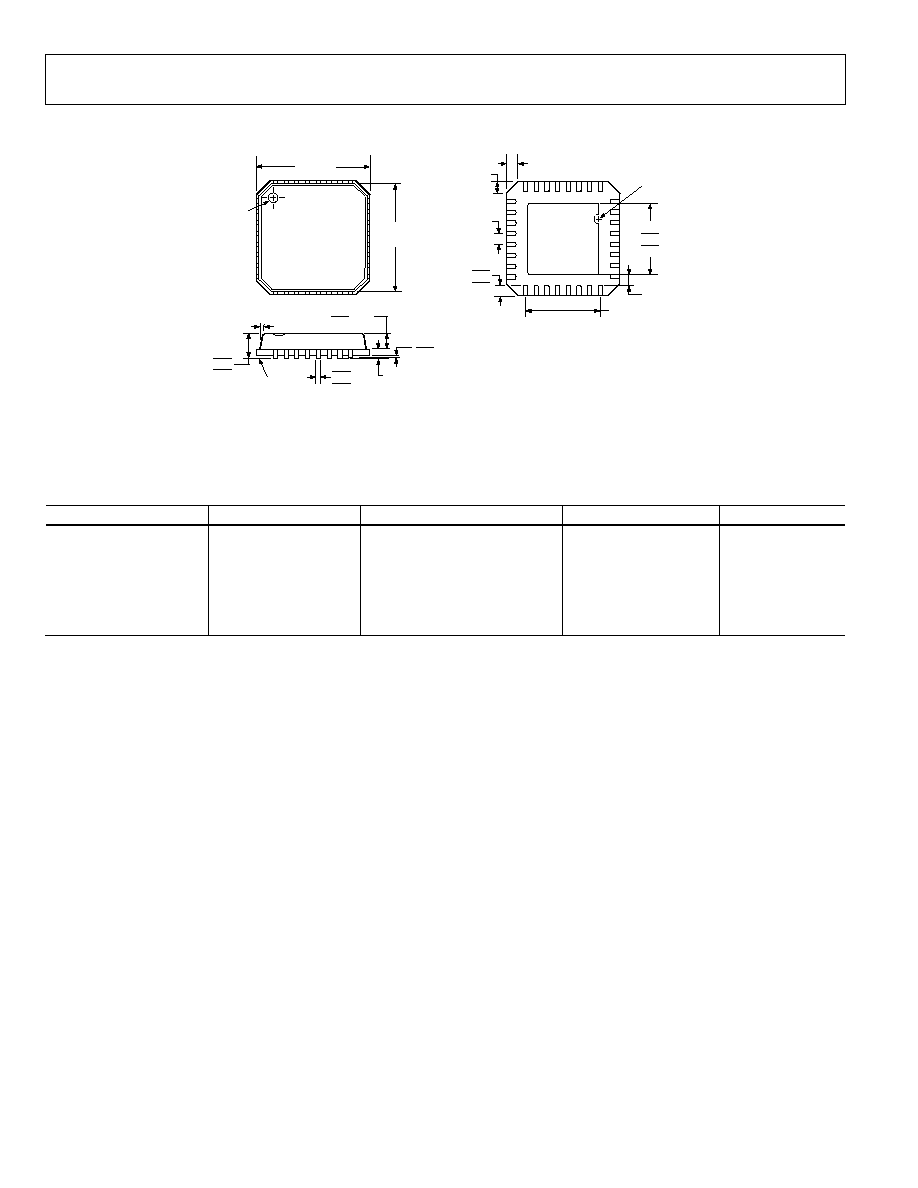
AD7142
Rev. 0 | Page 66 of 68
OUTLINE DIMENSIONS
COMPLIANT TO JEDEC STANDARDS MO-220-VHHD-2
0.30
0.23
0.18
0.20 REF
0.80 MAX
0.65 TYP
0.05 MAX
0.02 NOM
12° MAX
1.00
0.85
0.80
SEATING
PLANE
COPLANARITY
0.08
1
32
8
9
25
24
16
17
0.50
0.40
0.30
3.50 REF
0.50
BSC
PIN 1
INDICATOR
TOP
VIEW
5.00
BSC SQ
4.75
BSC SQ
3.25
3.10 SQ
2.95
PIN 1
INDICATOR
0.60 MAX
0.60 MAX
0.25 MIN
EXPOSED
PAD
(BOTTOM VIEW)
Figure 58. 32-Lead Frame Chip Scale Package [LFCSP_VQ]
5 mm × 5 mm Very Thin Quad
(CP-32-2)
Dimensions shown in millimeters
ORDERING GUIDE
Model
Temperature Range
Serial Interface Description
Package Description
Package Option
AD7142ACPZ-REEL
1
40°C to +85°C
SPI Interface
32-Lead LFCSP_VQ
CP-32-2
AD7142ACPZ-500RL7
1
40°C to +85°C
SPI Interface
32-Lead LFCSP_VQ
CP-32-2
AD7142ACPZ-1REEL
1
40°C to +85°C
I
2
C Interface
32-Lead LFCSP_VQ
CP-32-2
AD7142ACPZ-1500RL7
1
40°C to +85°C
I
2
C Interface
32-Lead LFCSP_VQ
CP-32-2
EVAL-AD7142EB
0°C to +85°C
SPI Interface
Evaluation Board
EVAL-AD7142-1EB
0°C to +85°C
I
2
C Interface
Evaluation Board
1
Z = Pb-free part.

AD7142
Rev. 0 | Page 67 of 68
NOTES

AD7142
Rev. 0 | Page 68 of 68
T
NOTES
Purchase of licensed I
2
C components of Analog Devices or one of its sublicensed Associated Companies conveys a license for the purchaser under the Philips I
2
C Patent
Rights to use these components in an I
2
C system, provided that the system conforms to the I
2
C Standard Specification as defined by Philips.
©2006 Analog Devices, Inc. All rights reserved. Trademarks and
registered trademarks are the property of their respective owners.
D05702-0-6/06(0)
TTT
Document Outline
- þÿ
- þÿ
- FUNCTIONAL BLOCK DIAGRAM
- þÿ
- þÿ
- þÿ
- þÿ
- þÿ
- þÿ
- þÿ
- þÿ
- þÿ
- þÿ
- þÿ
- þÿ
- þÿ
- þÿ
- þÿ
- þÿ
- GPIO INT OUTPUT CONTROL
- þÿ
- þÿ
- þÿ
- þÿ
- þÿ
- þÿ
- þÿ
- þÿ
- BANK 2 REGISTERS
- BANK 3 REGISTERS
- þÿ