 | –≠–ª–µ–∫—Ç—Ä–æ–Ω–Ω—ã–π –∫–æ–º–ø–æ–Ω–µ–Ω—Ç: AD721JP | –°–∫–∞—á–∞—Ç—å:  PDF PDF  ZIP ZIP |
Document Outline
- Specifications
- Pinout
- Package drawings
- Ordering Guide
- Features
- Applications
- Product Description
- Absolute Maximum Ratings
- Functional Block Diagram
- Circuit Description
- Typical Characteristics
- THEORY OF OPERATION
- APPLYING THE AD720/AD721
- DIAGRAMS
- AD720/AD721 Evaluation Setup
- Composite Output Differential Phase and Gain, NTSC (Nulled to Chroma Output)
- Modulated Pulse and Bar, NTSC
- 100% Color Bars, NTSC
- Multipulse, NTSC
- Horizontal Timing, NTSC
- Horizontal Timing, PAL
- AD720/AD721 Functional Block Diagram
- AD720 Application
- AD721 Application
- NTSC and PAL Timing for Valid Horizontal Sync Pulses

a
FUNCTIONAL BLOCK DIAGRAM
SYNC
DECODER
BURST
C-SYNC
4FSC
ENCD
RED
GREEN
BLUE
QUADRATURE
DECODER
DELAYED C-SYNC
SC 90
∞
SC 0
∞
CLOCK
AT 8FSC
DC
RESTORE
AND C-SYNC
INSERTION
5MHz
2-POLE
LP POST-
FILTER
COMPOSITE OUTPUT*
≠0.572V TO 2V NTSC
≠0.6V TO 2V PAL
LUMINANCE OUTPUT*
≠0.572V TO 1.43V NTSC
≠0.6V TO 1.4V PAL
CHROMINANCE OUTPUT*
572mVp-p NTSC
600mVp-p PAL
NTSC/
PAL
C-SYNC
DELAY
±
180
∞
(PAL ONLY)
RGB-TO-YUV
ENCODING
MATRIX
BURST
Y
U
V
SC 90
∞
/270
∞
5MHz
4-POLE LP
PRE-FILTER
1.2MHz
4-POLE
LPF
1.2MHz
4-POLE
LPF
SAMPLED-
DATA
DELAY LINE
3.6MHz (NTSC)
4.4MHz (PAL)
3-POLE LPF
X2
X2
X2
POWER AND GROUNDS
+5V
AGND
DGND
LOGIC
ANALOG
ANALOG ONLY
ANALOG
LOGIC
+5V
≠5V
*NOTE:
THE LUMINANCE, COMPOSITE, AND CHROMINANCE
OUTPUTS ARE AT TWICE NORMAL LEVELS FOR
DRIVING 75
REVERSE-TERMINATED LINES.
ASNC
NTSC/
PAL
BALANCED
MODULATORS
NTSC/
PAL
X2
X2
X2
ROUT
1.5Vp-p
GOUT
1.5Vp-p
BOUT
1.5Vp-p
AD721
(ONLY)
NTSC/
PAL
AD720/AD721
FEATURES
Composite Video Output
Chrominance and Luminance (S-Video) Outputs
No External Filters or Delay Lines Required
Drives 75
Reverse-Terminated Loads
Compact 28-Pin PLCC
Logic Selectable NTSC or PAL Encoding Modes
Automatically Selects Proper Chrominance Filter
Cutoff Frequency for Encoding Standard
Logic Selectable Encode or Power-Down Mode (AD720
Only)
Logic Selectable Encode or Bypass Mode (AD721 Only)
Low Power: 200 mW typical
APPLICATIONS
RGB to NTSC or PAL Encoding
Drive RGB Signals into 75
Load (AD721 Only)
PRODUCT DESCRIPTION
The AD720 and AD721 RGB to NTSC/PAL Encoders convert
red, green and blue color component signals into their corre-
sponding luminance (baseband amplitude) and chrominance
(subcarrier amplitude and phase) signals in accordance with
either NTSC or PAL standards. These two outputs are also
combined to provide a composite video output. All three out-
puts are available separately at voltages of twice the standard
signal levels as required for driving 75
reverse terminated
cables. The AD721 also features a bypass mode, in which the
RGB inputs may bypass the encoder section of the IC via three
gain-of-two amplifiers suitable for driving 75
reverse termi-
nated cables.
The AD720 and AD721 provide a complete, fully calibrated
function, requiring only termination resistors, bypass capacitors,
a clock input at four times the subcarrier frequency, and a com-
posite sync pulse. There are two control inputs: one input
selects the TV standard (NTSC/PAL) and the other (ENCD)
powers down most sections of the chip when the encoding func-
tion is not in use (AD720) or activates the triple bypass buffer to
drive the RGB signals when RGB encoding is not required
(AD721). All logical inputs are CMOS compatible. The chip
operates from
±
5 V supplies.
(continued on page 5)
RGB to NTSC/PAL Encoders
One Technology Way, P.O. Box 9106, Norwood. MA 02062-9106, U.S.A.
Tel: 617/329-4700
Fax: 617/326-8703
REV. 0
Information furnished by Analog Devices is believed to be accurate and
reliable. However, no responsibility is assumed by Analog Devices for its
use, nor for any infringements of patents or other rights of third parties
which may result from its use. No license is granted by implication or
otherwise under any patent or patent rights of Analog Devices.

REV. 0
≠2≠
Parameter
Conditions
Min
Typ
Max
Unit
SIGNAL INPUTS (RDIN, GRIN, BLIN)
Input Amplitude
NTSC
714
mV
PAL
700
mV
Input Resistances
1
RDIN with Respect to AGND
2.3
k
GRIN with Respect to AGND
4.2
k
BLIN with Respect to AGND
4.2
k
Input Capacitance
5
pF
LOGIC INPUTS (C-SYNC, 4FSC, ENCD, NTSC)
Logic LO Input Voltage
1
V
Logic HI Input Voltage
4
V
Logic LO Input Current (DC)
<1
µ
A
Logic HI Input Current (DC)
<1
µ
A
BYPASS AMPLIFIERS (AD721 Only)
Gain Error
Nominal Gain of
◊
2
2
≠5
+5
%
Small Signal ≠3 dB Bandwidth
100
MHz
Output Offset Voltage (Active State)
≠50
+50
mV
Output Voltage (Inactive State)
≠50
+50
mV
VIDEO OUTPUTS
3
(LUMA, CRMA, CMPS)
Luminance (LUMA) Output
Bandwidth
5
MHz
Gain Error
≠5
±
1
+5
%
Linearity
±
0.1
%
Sync Level
NTSC
252
286
320
mV
PAL
300
mV
Chrominance (CRMA) Output
Bandwidth
NTSC
3.6
MHz
PAL
4.4
MHz
Color Burst Amplitude
NTSC
257
286
315
mV p-p
PAL
300
mV p-p
Absolute Gain Error
≠15
±
5
+15
%
Absolute Phase Error
±
3
Degrees
Chroma/Luma Time Alignment
4
NTSC
≠170
ns
Composite Output
Absolute Gain Error
≠5
±
1
+5
%
Differential Gain
With Respect to Chroma Channel
0.1
%
Differential Phase
With Respect to Chroma Channel
0.1
Degrees
Output Offset Voltage
Chroma, Luma, or Composite Outputs
50
100
mV
Chroma Feedthrough
Monochrome Input
20
55
mV p-p
POWER SUPPLIES (APOS, DPOS, VNEG)
Recommended Supply Range
Dual Supply
±
4.75
±
5.25
V
Full Output Current
5
≠5 V Supply
35
mA
+5 V Supply
67
mA
Zero Signal Quiescent Current
≠5 V Supply
10
20
35
mA
+5 V Supply
10
20
35
mA
Bypass Mode Quiescent Current
≠5 V Supply
14
20
mA
(AD721 Only)
+5 V Supply
14
20
mA
AD720/AD721≠SPECIFICATIONS
NOTES
1
Input scaling resistors provide best scaling accuracy when source resistance is 37.5
(75
reverse-terminated input).
2
Required for driving a 75
double reverse terminated load.
3
All outputs are measured at a reverse-terminated load; voltages at IC pins are twice those specified here.
4
This is a predistortion (per FCC specifications) that compensates for the chroma/luma delay in the low-pass filter that separates the luminance and chrominance
signals in a television receiver.
5
CRMA, LUMA, and CMPS outputs are all connected to 75
reverse-terminated loads; full-white signal for entire field.
Specifications shown in boldface are tested on all production units at final electrical test. Results from those tests are used to calculate outgoing quality levels. All min
and max specifications are guaranteed, although only those shown in boldface are tested on all production units.
Specifications subject to change without notice.
(T
A
= +25
∞
C and supplies =
±
5 V unless otherwise noted)

AD720/AD721
REV. 0
≠3≠
PIN DESCRIPTIONS
Pin Mnemonic*
Description*
1
(NC) GOUT
(No Connection) Green Bypass Buffer
2
(NC) APOS
(No Connection) Analog Positive Supply; +5 V
±
5%
3
(NC) ROUT
(No Connection) Red Bypass Buffer
4
AGND
Analog Ground Connection
5
ENCD
A Logical High Enables the NTSC/PAL Encode
Mode (A Logical Low Powers Down the Chip)
A Logical Low Enables the RGB Bypass Mode
6
RDIN
Red Component Video Input
0 mV to 714 mV for NTSC
0 mV to 700 mV for PAL
7
AGND
Analog Ground Connection
8
GRIN
Green Component Video Input
0 mV to 714 mV for NTSC
0 mV to 700 mV for PAL
9
AGND
Analog Ground Connection
10
BLIN
Blue Component Video Input
0 mV to 714 mV for NTSC
0 mV to 700 mV for PAL
11
STND
A Logical High Input Selects NTSC Encoding
A Logical Low Input Selects PAL Encoding
CMOS Logic Levels
12
AGND
Analog Ground Connection
13
CRMA
Chrominance Output; Subcarrier Only**
572 mV Peak-to-Peak for NTSC
600 mV Peak-to-Peak for PAL
14
APOS
Analog Positive Supply; +5 V
±
5%
15
CMPS
Composite Video Output**
≠572 mV to 2 V for NTSC
≠600 mV to 2 V for PAL
16
APOS
Analog Positive Supply; +5 V
±
5%
17
LUMA
Luminance Plus SYNC Output**
≠572 mV to 1.43 V for NTSC
≠600 mV to 1.4 V for PAL
18
VNEG
System Negative Supply; ≠5 V
±
5%
19
DGND
Digital Ground Connection
20
4FSC
Clock Input at Four Times the Subcarrier Frequency
14.318 180 MHz for NTSC
17.734 480 MHz for PAL
CMOS Logic Levels
21
DPOS
Digital Positive Supply; +5 V
±
5%
22
ASNC
A Logical High Input Resets the Subcarrier Phase
Every Frame
A Logical Low Input Resets the Subcarrier Phase
Every Fourth Frame
CMOS Logic Levels
23
DPOS
Digital Positive Supply; +5 V
±
5%
24
SYNC
Input for Composite Television
Synchronization Pulses
Negative Sync Pulses
CMOS Logic Levels
25
DGND
Digital Ground Connections (One of Two)
26
VNEG
System Negative Supply; ≠5 V
±
5%
27
(NC) BOUT
(No Connection) Blue Bypass Buffer
28
APOS
Analog Positive Supply; +5 V
±
5%
*( ) pertain only to AD720.
**The luminance, chrominance, and composite outputs are at twice normal
levels for driving 75
reverse-terminated lines.
ORDERING GUIDE
Temperature
Package
Model
Range
Package
Option
AD720JP
0
∞
C to +70
∞
C
28-Pin PLCC
P-28A
AD721JP
0
∞
C to +70
∞
C
28-Pin PLCC
P-28A
PIN CONNECTIONS
28-Lead Plastic Leaded Chip Carrier (PLCC) Package
P-28A
AD720/AD721
RGB TO NTSC/PAL
ENCODER
5
6
7
8
9
10
11
28
27
26
1
2
3
4
25
24
23
22
21
20
19
12
13
14
15
16
17
18
DGND
SYNC
DPOS
ASNC
DPOS
4FSC
DGND
ENCD
RDIN
AGND
GRIN
AGND
BLIN
STND
AGND
ROUT (NC)
APOS (NC)
GOUT (NC)
APOS
BOUT (NC)
VNEG
AGND
CRMA
APOS
CMPS
LUMA
VNEG
APOS
NOTE:
CONNECTIONS IN ( ) PERTAIN ONLY TO AD720
ABSOLUTE MAXIMUM RATINGS*
Supply Voltage
±
V
S
. . . . . . . . . . . . . . . . . . . . . . . . . . . . .
±
6 V
Internal Power Dissipation . . . . . . . . . . . . . . . . . . . . . . 600 mW
Operating Temperature Range . . . . . . . . . . . . . . 0
∞
C to +70
∞
C
Storage Temperature Range . . . . . . . . . . . . ≠65
∞
C to +150
∞
C
Lead Temperature, Soldering 60 sec . . . . . . . . . . . . . . +300
∞
C
NOTE
*Stresses above those listed under "Absolute Maximum Ratings" may cause
permanent damage to the device. This is a stress rating only, and functional
operation of the device at these or any other conditions above those indicated in the
operational section of this specification is not implied. Exposure to absolute
maximum rating conditions for extended rating conditions for extended periods
may affect device reliability.
Thermal characteristics: 28-pin plastic package:
JA
= 100
∞
C.
WARNING!
ESD SENSITIVE DEVICE
CAUTION
ESD (electrostatic discharge) sensitive device. Electrostatic charges as high as 4000 V readily
accumulate on the human body and test equipment and can discharge without detection.
Although the AD720/AD721 features proprietary ESD protection circuitry, permanent damage
may occur on devices subjected to high energy electrostatic discharges. Therefore, proper ESD
precautions are recommended to avoid performance degradation or loss of functionality.

75
75
TEKTRONIX TSG 300
COMPONENT VIDEO
WAVEFORM GENERATOR
AD720/AD721
RGB TO NTSC/PAL
ENCODER
SONY
MONITOR
MODEL 1342
TEKTRONIX 1910
COMPOSITE VIDEO
WAVEFORM GENERATOR
GENLOCK
RGB
3
COMPOSITE
SYNC
FSC
4FSC
PIXEL-CLOCK
GENERATOR
COMPOSITE VIDEO
TEKTRONIX VM700A
WAVEFORM MONITOR
Figure 1. AD720/AD721 Evaluation Setup
0.10
0.05
0.00
≠0.05
≠0.10
0.00
≠0.04
0.00
≠0.01
≠0.04
≠0.10
0.10
0.05
0.00
≠0.05
≠0.10
0.00
0.05
0.05
0.04
0.07
0.01
1ST
2ND
3RD
4TH
5TH
6TH
DG DP(NTSC) (SYNC = EXT)
FIELD = 1 LINE = 21
DIFFERENTIAL GAIN (%) MIN = ≠0.10; MAX = 0.00; p-p/MAX = 0.10
DIFFERENTIAL PHASE (
∞
) MIN = 0.00; MAX = 0.07; p-p = 0.07
Figure 2. Composite Output Differential Phase and Gain,
NTSC (Nulled to Chroma Output)
100.0
0.0
0.0
50.0
70.0
60.0
50.0
40.0
30.0
20.0
10.0
0.5
NOISE REDUCTION: 15.05dB
APL = 49.6%
525 LINE NTSC; NO FILTERING
SLOW CLAMP TO 0.00V AT 6.63
µ
s
SYNC = SOURCE
FRAMES SELECTED: 1 2
MICROSECONDS/PRECISION MODE OFF
VOLTS
IRE:FLT
Figure 3. Modulated Pulse and Bar, NTSC
0.0
70.0
60.0
50.0
40.0
30.0
20.0
10.0
MICROSECONDS
FRAMES SELECTED: 1 2; APL = 45.8%
525 LINE NTSC; NO FILTERING
SLOW CLAMP TO 0.00V AT 6.63
µ
s
PRECISION MODE OFF
SYNC = SOURCE
100.0
0.0
0.0
50.0
70.0
60.0
50.0
40.0
30.0
20.0
10.0
0.5
VOLTS
IRE:FLT
Figure 4. 100% Color Bars, NTSC
0.0
70.0
60.0
50.0
40.0
30.0
20.0
10.0
MICROSECONDS
FRAMES SELECTED: 1 2; APL = 11.3%
525 LINE NTSC; NO FILTERING
SLOW CLAMP TO 0.00V AT 6.63
µ
s
PRECISION MODE OFF
SYNC = SOURCE
100.0
0.0
0.0
50.0
70.0
60.0
50.0
40.0
30.0
20.0
10.0
0.5
VOLTS
IRE:FLT
Figure 5. Multipulse, NTSC
5.35
µ
s
4.82
µ
s
8.0
CYCLES
39.4 IRE
85ns
73ns
H TIMING MEASUREMENT RS-170A (NTSC)
FIELD = 1 LINE = 22
39.2 IRE
AVERAGE 32 TO 32
Figure 6. Horizontal Timing, NTSC
4.82
µ
s
1.98
µ
s
292.1mV
81ns
AVERAGE 32 TO 32
302.2mV
H TIMING (PAL)
LINE = 17
82ns
5.52
µ
s
Figure 7. Horizontal Timing, PAL
AD720/AD721≠Typical Characteristics
≠4≠
REV. 0
AD720/AD721
REV. 0
≠5≠
(continued from page 1)
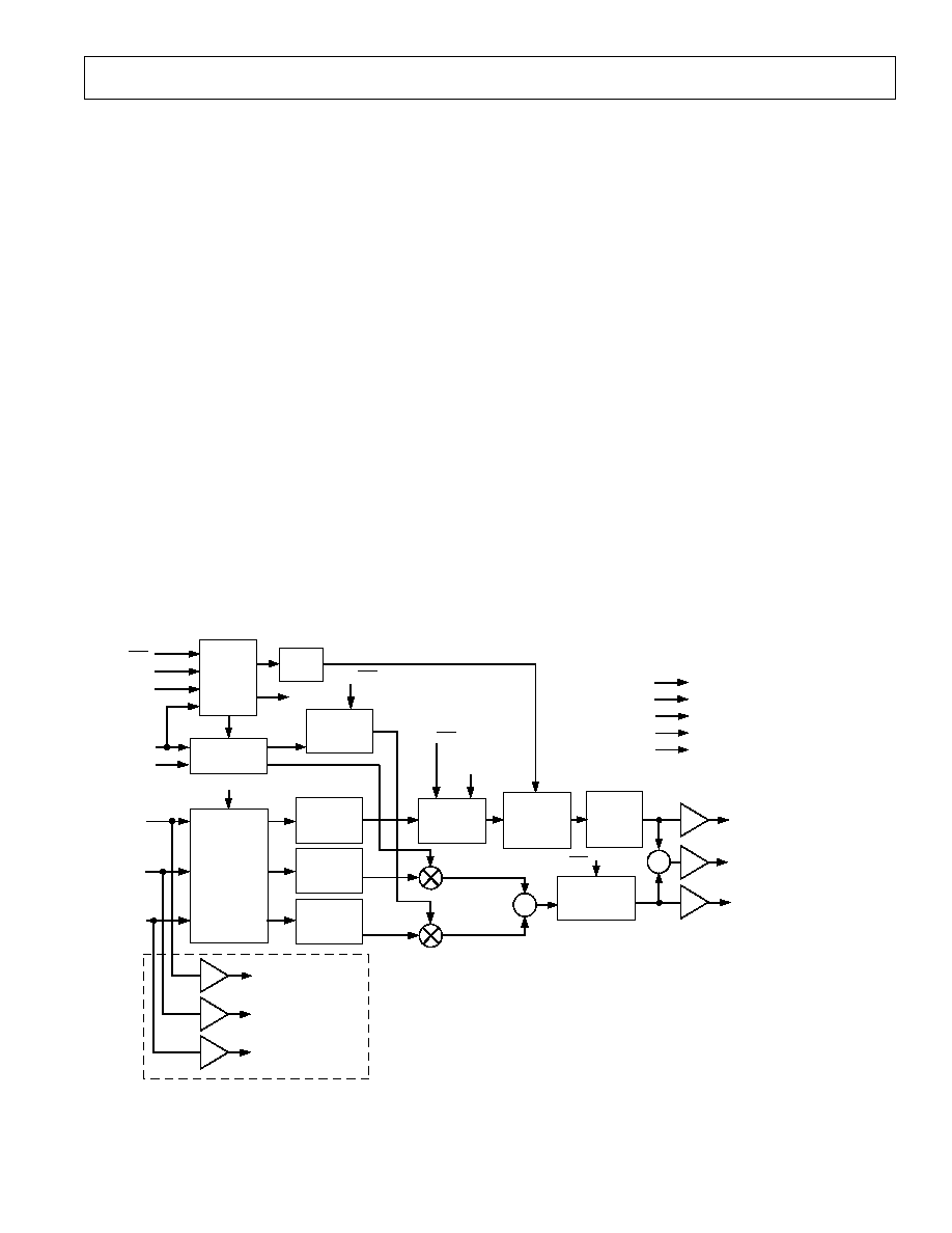
All required low-pass filters are on chip. After the input signals
pass through a precision RGB to YUV encoding matrix, two on-
chip low-pass filters limit the bandwidth of the U and V color
difference signals to 1.2 MHz prior to quadrature modulation of
the color subcarrier; a third low-pass filter at 3.6 MHz (NTSC)
or 4.4 MHz (PAL) follows the modulators to limit the harmonic
content of the output.
Delays in the U and V chroma filters are matched by an on-chip
sampled data delay line in the Y signal path; to prevent aliasing,
prefilter at 5 MHz is included ahead of the delay line and a post
filter at 5 MHz is added after the delay line to suppress harmon-
ics in the output. These low-pass filters are optimized for mini-
mum pulse overshoot. The overall delay is about 170 ns, which
precompensates for delays in the filters used to decode the
NTSC or PAL signal in a television receiver. (This precompen-
sation delay is already present in TV broadcasts.)
The AD720 and AD721 are available in a 28-pin plastic leaded
chip carrier for the 0
∞
C to +70
∞
C commercial temperature range.
THEORY OF OPERATION
Referring to the AD720/AD721 block diagram (Figure 8), the
RGB inputs (each 0 mV to 714 mV in NTSC or 0 mV to
700 mV in PAL) are first encoded into luminance and color
difference signals. The luminance signal is called the "Y"
signal and the color-difference signals are called U and V. The
RGB inputs are encoded into the YUV format using the
transformation
Y = 0.299R + 0.587G + 0.114B
U = 0.493 (B-Y)
V = 0.877 (R-Y)
For NTSC operation, the chroma amplitude is increased by the
factor 1.06 prior to summation with the luminance output. The
burst signal is inserted into the Y channel in the encoding matrix.
The three outputs of the encoding matrix, now transformed into Y,
U, and V components, take two paths. The Y (luminance) signal is
passed through a delay line consisting of a prefilter, a sampled-data
delay line, and a post filter. The pre- and post-filters prevent
aliasing of harmonics back into the baseband video. The overall de-
lay is a nominal ≠170 ns relative to the chrominance signal, in
keeping with broadcast requirements to compensate for delays in-
troduced by the filters in the decoding process.
The U and V components pass through 4-pole modified Bessel
low-pass filters with a 1.2 MHz ≠3 dB frequency to prevent
aliasing in the balanced modulators, where they modulate a
3.579 545 000 MHz (NTSC) or 4.433 618 750 MHz (PAL)
signal via a pair of balanced modulators driven in quadrature by
the color subcarrier.
The AD720/AD721 4FSC input drives a digital divide-by-4 cir-
cuit (two flip-flops) to create the quadrature signal. The refer-
ence phase 0
∞
is used for the U signal. In the NTSC mode, the
V signal is modulated at 90
∞
, but in the PAL mode, the V
modulation input alternates between 90
∞
and 270
∞
at half the
line rate as required by the PAL standard. The outputs of the
balanced modulators are summed and low-pass filtered to re-
move harmonics.
SYNC
DECODER
BURST
C-SYNC
4FSC
ENCD
RED
GREEN
BLUE
QUADRATURE
DECODER
DELAYED C-SYNC
SC 90
∞
SC 0
∞
CLOCK
AT 8FSC
DC
RESTORE
AND C-SYNC
INSERTION
5MHz
2-POLE
LP POST-
FILTER
COMPOSITE OUTPUT*
≠0.572V TO 2V NTSC
≠0.6V TO 2V PAL
LUMINANCE OUTPUT*
≠0.572V TO 1.43V NTSC
≠0.6V TO 1.4V PAL
CHROMINANCE OUTPUT*
572mVp-p NTSC
600mVp-p PAL
NTSC/
PAL
C-SYNC
DELAY
±
180
∞
(PAL ONLY)
RGB-TO-YUV
ENCODING
MATRIX
BURST
Y
U
V
SC 90
∞
/270
∞
5MHz
4-POLE LP
PRE-FILTER
1.2MHz
4-POLE
LPF
1.2MHz
4-POLE
LPF
SAMPLED-
DATA
DELAY LINE
3.6MHz (NTSC)
4.4MHz (PAL)
3-POLE LPF
X2
X2
X2
POWER AND GROUNDS
+5V
AGND
DGND
LOGIC
ANALOG
ANALOG ONLY
ANALOG
LOGIC
+5V
≠5V
*NOTE:
THE LUMINANCE, COMPOSITE, AND CHROMINANCE
OUTPUTS ARE AT TWICE NORMAL LEVELS FOR
DRIVING 75
REVERSE-TERMINATED LINES.
ASNC
NTSC/
PAL
BALANCED
MODULATORS
NTSC/
PAL
X2
X2
X2
ROUT
1.5Vp-p
GOUT
1.5Vp-p
BOUT
1.5Vp-p
AD721
(ONLY)
NTSC/
PAL
Figure 8. AD720/AD721 Functional Block Diagram