 | –≠–ª–µ–∫—Ç—Ä–æ–Ω–Ω—ã–π –∫–æ–º–ø–æ–Ω–µ–Ω—Ç: AD7237A | –°–∫–∞—á–∞—Ç—å:  PDF PDF  ZIP ZIP |

FUNCTIONAL BLOCK DIAGRAMS
REV. 0
Information furnished by Analog Devices is believed to be accurate and
reliable. However, no responsibility is assumed by Analog Devices for its
use, nor for any infringements of patents or other rights of third parties
which may result from its use. No license is granted by implication or
otherwise under any patent or patent rights of Analog Devices.
a
LC
2
MOS
Dual 12-Bit DACPORTs
AD7237A/AD7247A
FEATURES
Complete Dual 12-Bit DAC Comprising
Two 12-Bit CMOS DACs
On-Chip Voltage Reference
Output Amplifiers
Reference Buffer Amplifiers
Improved AD7237/AD7247:
12 V to 15 V Operation
Faster Interface ≠30 ns typ Data Setup Time
Parallel Loading Structure: AD7247A
(8+4) Loading Structure: AD7237A
Single or Dual Supply Operation
Low Power--165 mW typ in Single Supply
One Technology Way, P.O. Box 9106, Norwood, MA 02062-9106, U.S.A.
Tel: 617/329-4700
Fax: 617/326-8703
PRODUCT HIGHLIGHTS
1. The AD7237A/AD7247A is a dual 12-bit DACPORT
Æ
on a
single chip. This single chip design and small package size
offer considerable space saving and increased reliability over
multichip designs.
2. The improved interface times of the parts allow easy, direct
interfacing to most modern microprocessors, whether they
have 8-bit or 16-bit data bus structures.
3. The AD7237A/AD7247A features a wide power supply
range allowing operation from 12 V supplies.
DACPORT is a registered trademark of Analog Devices, Inc.
GENERAL DESCRIPTION
The AD7237A/AD7247A is an enhanced version of the industry
standard AD7237/AD7247. Improvements include operation
from 12 V to 15 V supplies, faster interface times and better
reference variations with V
DD
. Additional features include faster
settling times.
The AD7237A/AD7247A is a complete, dual, 12-bit, voltage
output digital-to-analog converter with output amplifiers and
Zener voltage reference on a monolithic CMOS chip. No exter-
nal user trims are required to achieve full specified performance.
Both parts are microprocessor compatible, with high speed data
latches and interface logic. The AD7247A accepts 12-bit paral-
lel data which is loaded into the respective DAC latch using the
WR
input and a separate Chip Select input for each DAC. The
AD7237A has a double buffered interface structure and an 8-bit
wide data bus with data loaded to the respective input latch in
two write operations. An asynchronous LDAC signal on the
AD7237A updates the DAC latches and analog outputs.
A REF OUT/REF IN function is provided which allows either
the on-chip 5 V reference or an external reference to be used as
a reference voltage for the part. For single supply operation, two
output ranges of 0 V to +5 V and 0 V to +10 V are available,
while these two ranges plus an additional
±
5 V range are avail-
able with dual supplies. The output amplifiers are capable of de-
veloping +10 V across a 2 k
load to GND.
The AD7237A/AD7247A is fabricated in Linear Compatible
CMOS (LC
2
MOS), an advanced, mixed technology process
that combines precision bipolar circuits with low power CMOS
logic. Both parts are available in a 24-pin, 0.3" wide plastic and
hermetic dual-in-line package (DIP) and are also packaged in a
24-lead small outline (SOIC) package.

REV. 0
≠2≠
AD7237A/AD7247A≠SPECIFICATIONS
(V
DD
= +12 V to +15 V,
1
V
SS
= 0 V or ≠12 V to ≠15 V,
1
AGND =
DGND = 0 V [AD7237A], GND = 0 V [AD7247A], REF IN = +5 V,
Parameter
A
2
B
2
T
2
Units
Test Conditions/Comments
STATIC PERFORMANCE
Resolution
12
12
12
Bits
Relative Accuracy
3
±
1
±
1/2
±
1/2
LSB max
Differential Nonlinearity
3
±
0.9
±
0.9
±
0.9
LSB max
Guaranteed Monotonic
Unipolar Offset Error
3
±
3
±
3
±
4
LSB max
V
SS
= 0 V or ≠12 V to ≠15 V
4
. DAC Latch Contents All 0s
Bipolar Zero Error
3
±
6
±
4
±
6
LSB max
V
SS
= ≠12 V to ≠15 V
4
. DAC Latch Contents
1000 0000 0000
Full-Scale Error
3, 5
±
5
±
5
±
6
LSB max
Full-Scale Mismatch
5
±
1
±
1
±
1
LSB typ
REFERENCE OUTPUT
REF OUT
4.97/5.03
4.97/5.03
4.95/5.05
V min/max
Reference Temperature
Coefficient
±
25
±
25
±
25
ppm/
∞
C typ
Reference Load Change
(
REF OUT vs.
I)
≠1
≠1
≠1
mV max
Reference Load Current Change (0-100
µ
A)
REFERENCE INPUT
Reference Input Range
4.75/5.25
4.75/5.25
4.75/5.25
V min/max
5 V
±
5%
Input Current
6
±
5
±
5
±
5
µ
A max
DIGITAL INPUTS
Input High Voltage, V
INH
2.4
2.4
2.4
V min
Input Low Voltage, V
INL
0.8
0.8
0.8
V max
Input Current
I
IN
(Data Inputs)
±
10
±
10
±
10
µ
A max
V
IN
= 0 V to V
DD
Input Capacitance
6
8
8
8
pF max
ANALOG OUTPUTS
Output Range Resistors
15/30
15/30
15/30
k
min/max
Output Voltage Ranges
7
+5, +10
+5, +10
V
Single Supply; (V
SS
= 0 V)
Output Voltage Ranges
7
+5, +10,
±
5
+5, +10,
±
5
+5, +10,
±
5
Dual Supply; (V
SS
= ≠12 V to ≠15 V
4
)
DC Output Impedance
0.5
0.5
0.5
typ
AC CHARACTERISTICS
6
Voltage Output Settling Time
Settling Time to Within
±
1/2 LSB of Final Value
Positive Full-Scale Change
8
8
10
µ
s max
DAC Latch all 0s to all 1s. Typically 5
µ
s
Negative Full-Scale Change 8
8
10
µ
s max
DAC Latch all 1s to all 0s. Typically 5
µ
s
V
SS
= ≠12 V to ≠15 V
4
.
Digital-to-Analog Glitch
Impulse
3
30
30
30
nV secs typ
DAC Latch Contents Toggled Between all 0s and all 1s
Digital Feedthrough
3
10
10
10
nV secs typ
Digital Crosstalk
3
30
30
30
nV secs typ
POWER REQUIREMENTS
V
DD
+10.8/+16.5 +11.4/+15.75 +11.4/+15.75 V min/max
For Specified Performance Unless Otherwise Stated
V
SS
≠10.8/≠16.5
≠11.4/≠15.75 ≠11.4/≠15.75
V min/max
For Specified Performance Unless Otherwise Stated
I
DD
15
15
15
mA max
Output Unloaded. Typically 10 mA
I
SS
(Dual Supplies)
5
5
5
mA max
Output Unloaded. Typically 3 mA
NOTES
1
Power Supply tolerance is
±
10% for A version and
±
5% for B and T versions.
2
Temperature ranges are as follows: A, B Versions, ≠40
∞
C to +85
∞
C; T Version, ≠55
∞
C to +125
∞
C.
3
See Terminology.
4
With appropriate power supply tolerances.
5
Measured with respect to REF IN and includes unipolar/bipolar offset error.
6
Sample tested @ +25
∞
C to ensure compliance.
7
0 V to +10 V range is only available with V
DD
14.25 V.
Specifications subject to change without notice.
R
L
= 2 k
, C
L
= 100 pF. All specifications T
MIN
to T
MAX
unless otherwise noted.)

AD7237A/AD7247A
REV. 0
≠3≠
TIMING CHARACTERISTICS
1, 2
Limit at T
MIN
, T
MAX
Limit at T
MIN
, T
MAX
Parameter
(A, B Versions)
(T Version)
Units
Conditions/Comments
t
1
0
0
ns min
CS
to WR Setup Time
t
2
0
0
ns min
CS
to WR Hold Time
t
3
80
100
ns min
WR
Pulse Width
t
4
80
80
ns min
Data Valid to WR Setup Time
t
5
4
10
10
ns min
Data Valid to WR Hold Time
t
6
0
0
ns min
Address to WR Setup Time
t
7
0
0
ns min
Address to WR Hold Time
t
8
5
80
100
ns min
LDAC
Pulse Width
NOTES
1
Sample tested at +25
∞
C to ensure compliance. All input signals are specified with tr = tf = 5 ns (10% to 90% of 5 V) and timed from a voltage level of 1.6 V.
2
See Figures 5 and 7.
3
Power Supply tolerance is
±
10% for A version and
±
5% for B and T versions.
4
If 0 ns < t
2
< 10 ns, add t
2
to t
5
. If t
2
10 ns, add 10 ns to t
5
.
5
AD7237A only.
ABSOLUTE MAXIMUM RATINGS
1
(T
A
= +25
∞
C unless otherwise noted)
V
DD
to GND (AD7247A) . . . . . . . . . . . . . . . . ≠0.3 V to +17 V
V
DD
to AGND, DGND (AD7237A) . . . . . . . . ≠0.3 V to +17 V
V
DD
to V
SS
. . . . . . . . . . . . . . . . . . . . . . . . . . . . ≠0.3 V to +34 V
AGND to DGND (AD7237A) . . . . . . . . . ≠0.3 V, V
DD
+0.3 V
V
OUTA
,
2
V
OUTB
2
to AGND (GND) . . V
SS
≠0.3 V to V
DD
+0.3 V
REF OUT to AGND (GND) . . . . . . . . . . . . . . . . . 0 V to V
DD
REF IN to AGND (GND) . . . . . . . . . . ≠0.3 V to V
DD
+0.3 V
Digital Inputs to DGND (GND) . . . . . . ≠0.3 V to V
DD
+0.3 V
Operating Temperature Range
Industrial (A, B Versions) . . . . . . . . . . . . . ≠40
∞
C to +85
∞
C
Extended (T Version) . . . . . . . . . . . . . . . ≠55
∞
C to +125
∞
C
Storage Temperature Range . . . . . . . . . . . . ≠65
∞
C to +150
∞
C
Lead Temperature (Soldering, 10 secs) . . . . . . . . . . . . +300
∞
C
Power Dissipation (Any Package) to +75
∞
C . . . . . . . 1000 mW
Derates above +75
∞
C by . . . . . . . . . . . . . . . . . . . . . 10 mW/
∞
C
NOTES
1
Stresses above those listed under "Absolute Maximum Ratings" may cause
permanent damage to the device. This is a stress rating only and functional
operation of the device at these or any other conditions above those listed in the
operational sections of this specification is not implied. Exposure to absolute
maximum rating conditions for extended periods may affect device reliability.
2
Short-circuit current is typically 80 mA. The outputs may be shorted to voltages
in this range provided the power dissipation of the package is not exceeded.
ORDERING GUIDE
Relative
Temperature
Accuracy
Package
Model
1
Range
(LSB)
Option
2
AD7237AAN
≠40
∞
C to +85
∞
C
±
1 max
N-24
AD7237ABN
≠40
∞
C to +85
∞
C
±
1/2 max
N-24
AD7237AAR
≠40
∞
C to +85
∞
C
±
1 max
R-24
AD7237ABR
≠40
∞
C to +85
∞
C
±
1/2 max
R-24
AD7237ATQ
≠55
∞
C to +125
∞
C
±
1/2 max
Q-24
AD7247AAN
≠40
∞
C to +85
∞
C
±
1 max
N-24
AD7247ABN
≠40
∞
C to +85
∞
C
±
1/2 max
N-24
AD7247AAR
≠40
∞
C to +85
∞
C
±
1 max
R-24
AD7247ABR
≠40
∞
C to +85
∞
C
±
1/2 max
R-24
AD7247ATQ
≠55
∞
C to +125
∞
C
±
1/2 max
Q-24
NOTES
1
To order MIL-STD-883, Class B processed parts, add /883B to part number.
Contact local sales office for military data sheet and availability.
2
N = Plastic DIP; Q = Cerdip; R = Small Outline (SOIC).
CAUTION
ESD (electrostatic discharge) sensitive device. Electrostatic charges as high as 4000 V readily
accumulate on the human body and test equipment and can discharge without detection.
Although the AD7237A/AD7247A features proprietary ESD protection circuitry, permanent
damage may occur on devices subjected to high energy electrostatic discharges. Therefore, proper
ESD precautions are recommended to avoid performance degradation or loss of functionality.
WARNING!
ESD SENSITIVE DEVICE
(V
DD
= +12 V to +15 V,
3
V
SS
= 0 V or ≠12 V to ≠15 V,
3
AGND = DGND = 0 V [AD7237A],
GND = 0 V [AD7247A])

AD7237A/AD7247A
REV. 0
≠4≠
AD7237A PIN FUNCTION DESCRIPTION (DIP PIN NUMBERS)
Pin
Mnemonic
Description
1
REF INA
Voltage Reference Input for DAC A. The reference voltage for DAC A is applied to this pin. It is internally
buffered before being applied to the DAC. The nominal reference voltage for correct operation of the
AD7237A is 5 V.
2
REF OUT
Voltage Reference Output. The internal 5 V analog reference is provided at this pin. To operate the part with
internal reference, REF OUT should be connected to REF INA, REF INB.
3
REF INB
Voltage Reference Input for DAC B. The reference voltage for DAC B is applied to this pin. It is internally
buffered before being applied to the DAC. The nominal reference voltage for correct operation of the
AD7237A is 5 V.
4
R
OFSB
Output Offset Resistor for DAC B. This input configures the output ranges for DAC B. It is connected to
V
OUTB
for the +5 V range, to AGND for the +10 V range and to REF INB for the
±
5 V range.
5
V
OUTB
Analog Output Voltage from DAC B. This is the buffer amplifier output voltage. Three different output
voltage ranges can be chosen: 0 V to +5 V, 0 V to +10 V and
±
5 V. The amplifier is capable of developing
+10 V across a 2 k
resistor to GND.
6
AGND
Analog Ground. Ground reference for DACs, reference and output buffer amplifiers.
7
DB7
Data Bit 7.
8-10
DB6-DB4
Data Bit 6 to Data Bit 4.
11
DB3
Data Bit 3/Data Bit 11 (MSB).
12
DGND
Digital Ground. Ground reference for digital circuitry.
13
DB2
Data Bit 2/Data Bit 10.
14
DB1
Data Bit 1/Data Bit 9.
15
DB0
Data Bit 0 (LSB)/Data Bit 8.
16
A0
Address Input. Least significant address input for input latches. A0 and A1 select which of the four input
latches data is written to (see Table II).
17
A1
Address Input. Most significant address input for input latches.
18
CS
Chip Select. Active low logic input. The device is selected when this input is active.
19
WR
Write Input. WR is an active low logic input which is used in conjunction with CS, A0 and A1 to write data
to the input latches.
20
LDAC
Load DAC. Logic input. A new word is loaded into the DAC latches from the respective input latches on the
falling edge of this signal.
21
V
DD
Positive Supply (+12 V to +15 V).
22
V
OUTA
Analog Output Voltage from DAC A. This is the buffer amplifier output voltage. Three different output
voltage ranges can be chosen: 0 V to +5 V, 0 V to +10 V and
±
5 V. The amplifier is capable of developing
+10 V across a 2 k
resistor to GND.
23
V
SS
Negative Supply (0 V or ≠12 V to ≠15 V).
24
R
OFSA
Output Offset Resistor for DAC A. This input configures the output ranges for DAC A. It is connected to
V
OUTA
for the +5 V range, to AGND for the +10 V range and to REF INA for the
±
5 V range.

AD7237A/AD7247A
REV. 0
≠5≠
AD7247A PIN FUNCTION DESCRIPTION (DIP PIN NUMBERS)
Pin
Mnemonic
Description
1
REF OUT
Voltage Reference Output. The internal 5 V analog reference is provided at this pin. To operate the part
with internal reference, REF OUT should be connected to REF IN.
2
R
OFSB
Output Offset Resistor for DAC B. This input configures the output ranges for DAC B. It is connected to
V
OUTB
for the +5 V range, to GND for the +10 V range and to REF IN for the
±
5 V range.
3
V
OUTB
Analog Output Voltage from DAC B. This is the buffer amplifier output voltage. Three different output
voltage ranges can be chosen: 0 V to +5 V, 0 V to +10 V and
±
5 V. The amplifier is capable of developing
+10 V across a 2 k
resistor to GND.
4
DB11
Data Bit 11 (MSB).
5
DB10
Data Bit 10.
6
GND
Ground. Ground reference for all on-chip circuitry.
7≠15
DB9-DB1
Data Bit 9 to Data Bit 1.
16
DB0
Data Bit 0 (LSB).
17
CSB
Chip Select Input for DAC B. Active low logic input. DAC B is selected when this input is active.
18
CSA
Chip Select Input for DAC A. Active low logic input. DAC A is selected when this input is active.
19
WR
Write Input. WR is an active low logic input which is used in conjunction with CSA and CSB to write data
to the DAC latches.
20
V
DD
Positive Supply (+12 V to +15 V).
21
V
OUTA
Analog Output Voltage from DAC A. This is the buffer amplifier output voltage. Three different output
voltage ranges can be chosen: 0 V to +5 V, 0 V to +10 V and
±
5 V. The amplifier is capable of developing
+10 V across a 2 k
resistor to GND.
22
V
SS
Negative Supply (0 V or ≠12 V to ≠15 V).
23
R
OFSA
Output Offset Resistor for DAC A. This input configures the output ranges for DAC A. It is connected to
V
OUTA
for the +5 V range, to GND for the +10 V range and to REF IN for the
±
5 V range.
24
REF IN
Voltage Reference Input. The common reference voltage for both DACs is applied to this pin. It is internally
buffered before being applied to both DACs. The nominal reference voltage for correct operation of the
AD7247A is 5 V.
AD7237A PIN CONFIGURATION
DIP and SOIC
AD7247A PIN CONFIGURATION
DIP and SOIC

AD7237A/AD7247A
REV. 0
≠6≠
TERMINOLOGY
RELATIVE ACCURACY (LINEARITY)
Relative Accuracy, or endpoint linearity, is a measure of the
maximum deviation of the DAC transfer function from a
straight line passing through the endpoints of the transfer func-
tion. It is measured after allowing for zero and full-scale errors
and is expressed in LSBs or as a percentage of full-scale reading.
DIFFERENTIAL NONLINEARITY
Differential Nonlinearity is the difference between the measured
change and the ideal 1 LSB change between any two adjacent
codes. A specified differential nonlinearity of
±
1 LSB or less
over the operating temperature range ensures monotonicity.
SINGLE SUPPLY LINEARITY AND GAIN ERROR
The output amplifiers of the AD7237A/AD7247A can have true
negative offsets even when the part is operated from a single
+12 V to +15 V supply. However, because the negative supply
rail (V
SS
) is 0 V, the output cannot actually go negative. Instead,
when the output offset voltage is negative, the output voltage
sits at 0 V, resulting in the transfer function shown in Figure 1.
This "knee" is an offset effect, not a linearity error, and the
transfer function would have followed the dotted line if the out-
put voltage could have gone negative.
Figure 1. Effect of Negative Offset (Single Supply)
Normally, linearity is measured between zero (all 0s input code)
and full scale (all 1s input code) after offset and full scale have
been adjusted out or allowed for, but this is not possible in
single supply operation if the offset is negative, due to the knee
in the transfer function. Instead, linearity of the AD7237A/
AD7247A in the unipolar mode is measured between full scale
and the lowest code which is guaranteed to produce a positive
output voltage. This code is calculated from the maximum
specification for negative offset, i.e., linearity is measured be-
tween Codes 3 and 4095.
UNIPOLAR OFFSET ERROR
Unipolar Offset Error is the measured output voltage from
V
OUTA
or V
OUTB
with all zeros loaded into the DAC latches
when the DACs are configured for unipolar output. It is a com-
bination of the offset errors of the DAC and output amplifier.
BIPOLAR ZERO ERROR
Bipolar Zero Error is the voltage measured at V
OUTA
or V
OUTB
when the DAC is connected in the bipolar mode and loaded
with code 2048. It is due to a combination of offset errors in the
DAC, amplifier offset and mismatch in the application resistors
around the amplifier.
FULL-SCALE ERROR
Full-Scale Error is a measure of the output error when the
amplifier output is at full scale (for the bipolar output range full
scale is either positive or negative full scale). It is measured with
respect to the reference input voltage and includes the offset
errors.
DIGITAL FEEDTHROUGH
Digital Feedthrough is the glitch impulse injected for the digital
inputs to the analog output when the data inputs change state,
but the data in the DAC latches is not changed.
For the AD7237A it is measured with LDAC held high. For the
AD7247A it is measured with CSA and CSB held high.
DIGITAL CROSSTALK
Digital crosstalk is the glitch impulse transferred to the output
of one converter due to a change in digital code to the DAC
latch of the other converter. It is specified in nV secs.
DIGITAL-TO-ANALOG GLITCH IMPULSE
This is the voltage spike that appears at the output of the DAC
when the digital code changes before the output settles to its fi-
nal value. The energy in the glitch is specified in nV secs and is
measured for a 1 LSB change around the major carry transition
(0111 1111 1111 to 1000 0000 0000).

AD7237A/AD7247A
REV. 0
≠7≠
Power Supply Current vs. Temperature
Noise Spectral Density vs. Frequency
Single Supply Sink Current vs. Output Voltage
DAC-to-DAC Linearity Matching
Power Supply Rejection Ratio vs. Frequency
Linearity vs. Power Supply Voltage

AD7237A/AD7247A
REV. 0
≠8≠
CIRCUIT INFORMATION
D/A Section
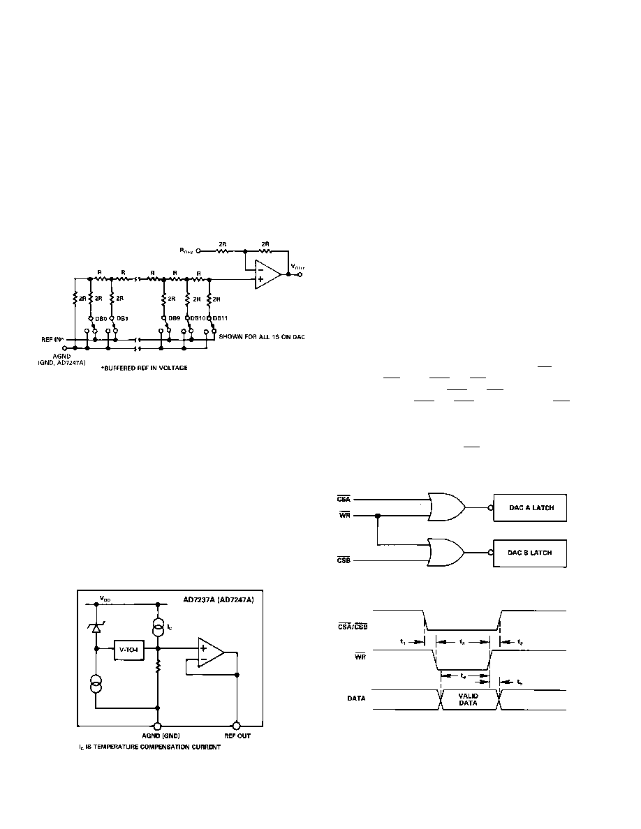
The AD7237A/AD7247A contains two 12-bit voltage-mode D/A
converters consisting of highly stable thin film resistors and high
speed NMOS single-pole, double-throw switches. The output
voltage from the converters has the same polarity as the refer-
ence voltage, REF IN, allowing single supply operation. The
simplified circuit diagram for one of the D/A converters is
shown in Figure 2.
The REF IN voltage is internally buffered by a unity gain
amplifier before being applied to the D/A converters. The D/A
converters are configured and scaled for a 5 V reference and the
device is tested with 5 V applied to REF IN.
Figure 2. D/A Simplified Circuit Diagram
Internal Reference
The AD7237A/AD7247A has an on-chip temperature compen-
sated buried Zener reference (see Figure 3) which is factory
trimmed to 5 V
±
30 mV (
±
50 mV for T Version). The reference
voltage is provided at the REF OUT pin. This reference can be
used to provide the reference voltage for the D/A converter (by
connecting the REF OUT pin to the REF IN pin) and the offset
voltage for bipolar outputs (by connecting REF OUT to R
OFS
).
The reference voltage can also be used as a reference for other
components and is capable of providing up to 500
µ
A to an ex-
ternal load. The maximum recommended capacitance on REF
OUT for normal operation is 50 pF. If the reference is required
for external use, it should be decoupled to AGND (GND) with
a 200
resistor in series with parallel combination of a 10
µ
F
tantalum capacitor and a 0.1
µ
F ceramic capacitor.
Figure 3. Internal Reference
External Reference
In some applications, the user may require a system reference or
some other external reference to drive the AD7237A/ AD7247A
reference input. References such as the AD586 5 V reference
provide the ideal external reference source for the AD7237A/
AD7247A (see Figure 9).
Op Amp Section
The output of the voltage-mode D/A converter is buffered by a
noninverting CMOS amplifier. The R
OFS
input allows different
output voltage ranges to be selected. The buffer amplifier is ca-
pable of developing +10 V across a 2 k
load to GND. The
output amplifier can be operated from a single +12 V to +15 V
supply by tying V
SS
= 0 V. The amplifier can also be operated
from dual supplies (
±
12 V to
±
15 V) to allow a bipolar output
range of ≠5 V to +5 V. The advantages of having dual supplies
for the unipolar output ranges are faster settling time to voltages
near 0 V, full sink capability of 2.5 mA maintained over the en-
tire output range and the elimination of the effects of negative
offsets on the transfer characteristic (outlined previously). A
plot of the single supply output sink capability of the amplifier is
shown in the Typical Performance Graphs section.
INTERFACE LOGIC INFORMATION--AD7247A
Table I shows the truth table for AD7247A operation. The part
contains a single, parallel 12-bit latch for each DAC. It can be
treated as two independent DACs, each with its own CS input
and a common WR input. CSA and WR control the loading of
data to the DAC A latch while CSB and WR control the loading
of the DAC B latch. If CSA and CSB are both low, with WR
low, the same data will be written to both DAC latches. All con-
trol signals are level triggered and therefore either or both
latches can be made transparent. Input data is latched to the re-
spective latch on the rising edge of WR. Figure 4 shows the in-
put control logic for the AD7247A, while the write cycle timing
diagram for the part is shown in Figure 5.
Figure 4. AD7247A Input Control Logic
Figure 5. AD7247A Write Cycle Timing Diagram

AD7237A/AD7247A
REV. 0
≠9≠
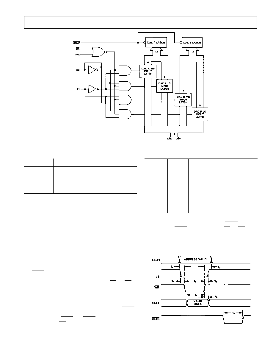
Figure 6. AD7237A Input Control Logic
Table II. AD7237A Truth Table
CS WR
A1 A0 LDAC Function
1
X
X X 1
No Data Transfer
X
1
X X 1
No Data Transfer
0
0
0
0
1
DAC A LS Input Latch Transparent
0
0
0
1
1
DAC A MS Input Latch Transparent
0
0
1
0
1
DAC B LS Input Latch Transparent
0
0
1
1
1
DAC B MS Input Latch Transparent
1
1
X X 0
DAC A and DAC B DAC Latches
Updated Simultaneously from the
Respective Input Latches
X = Don't Care.
However, care must be taken while exercising LDAC during a
write cycle. If an LDAC operation overlaps a CS and WR op-
eration, there is a possibility of invalid data being latched to the
output. To avoid this, LDAC must remain low after CS or WR
return high for a period equal to or greater than t
8
, the mini-
mum LDAC pulse width.
Figure 7. AD7237A Write Cycle Timing Diagram
Table I. AD7247A Truth Table
CSA
CSB
WR
Function
X
X
1
No Data Transfer
1
1
X
No Data Transfer
0
1
0
DAC A Latch Transparent
1
0
0
DAC B Latch Transparent
0
0
0
Both DAC Latches Transparent
X = Don't Care
INTERFACE LOGIC INFORMATION--AD7237A
The input loading structure on the AD7237A is configured for
interfacing to microprocessors with an 8-bit-wide data bus. The
part contains two 12-bit latches per DAC--an input latch and a
DAC latch. Each input latch is further subdivided into a least
significant 8-bit latch and a most significant 4-bit latch. Only
the data held in the DAC latches determines the outputs from
the part. The input control logic for the AD7237A is shown in
Figure 6, while the write cycle timing diagram is shown in
Figure 7.
CS
, WR, A0 and A1 control the loading of data to the input
latches. The eight data inputs accept right-justified data. Data
can be loaded to the input latches in any sequence. Provided
that LDAC is held high, there is no analog output change as a
result of loading data to the input latches. Address lines A0 and
A1 determine which latch data is loaded to when CS and WR
are low. The selection of the input latches is shown in the truth
table for AD7237A operation in Table II.
The LDAC input controls the transfer of 12-bit data from the
input latches to the DAC latches. Both DAC latches, and hence
both analog outputs, are updated at the same time. The LDAC
signal is level triggered, and data is latched into the DAC latch
on the rising edge of LDAC. The LDAC input is asynchronous
and independent of WR. This is useful in many applications
especially in the simultaneous updating of multiple AD7237As.

AD7237A/AD7247A
REV. 0
≠10≠
APPLYING THE AD7237A/AD7247A
The internal scaling resistors provided on the AD7237A/
AD7247A allow several output voltage ranges. The part can
produce unipolar output ranges of 0 V to +5 V or 0 V to +10 V
and a bipolar output range of
±
5 V. Connections for the various
ranges are outlined below. Since each DAC has its own R
OFS
input the two DACs on each part can be set up for different
output ranges.
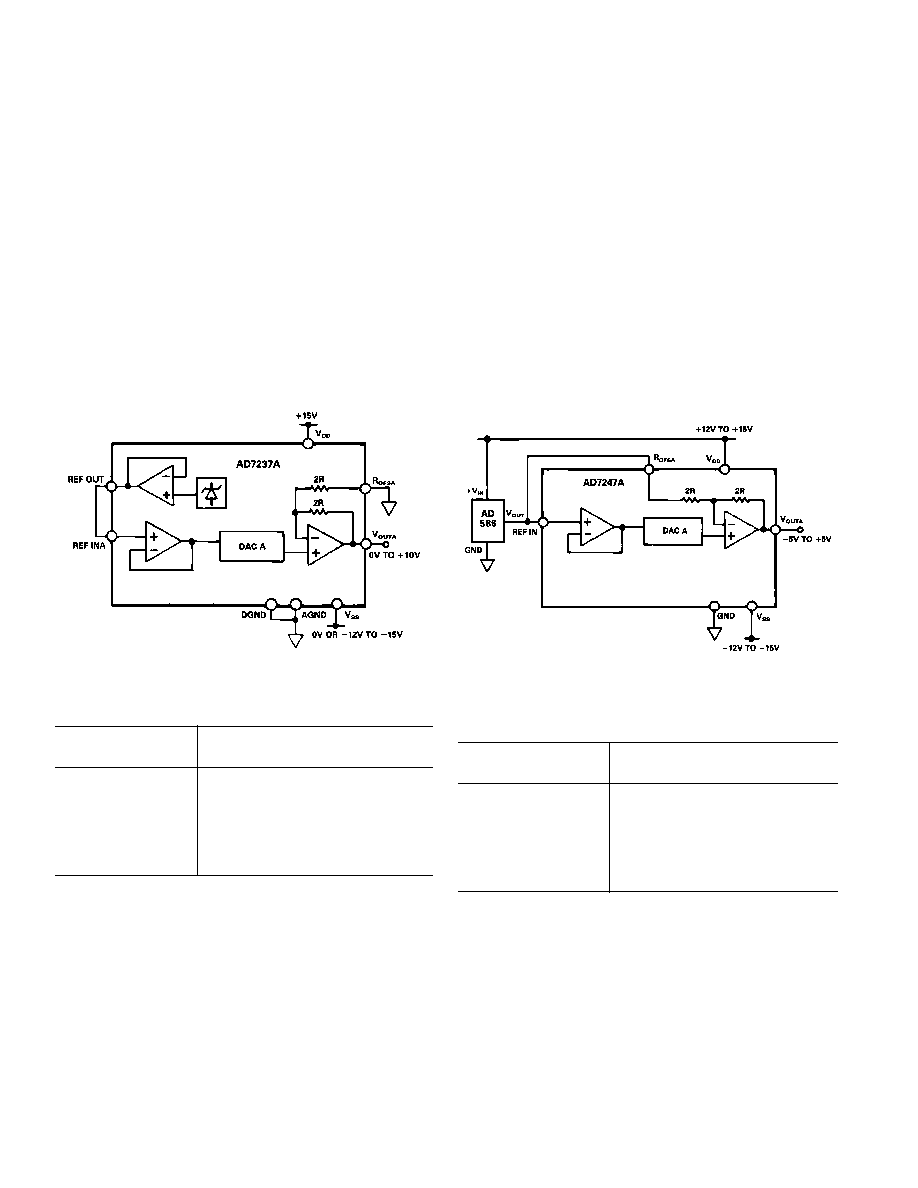
Unipolar (0 V to +10 V) Configuration
The first of the configurations provides an output voltage range
of 0 V to +10 V. This is achieved by connecting the output off-
set resistor, R
OFSA
, or R
OFSB
, to AGND (GND for AD7247A).
In this configuration, the AD7237A/AD7247A can be operated
from single or dual supplies. Figure 8 shows the connection dia-
gram for unipolar operation for DAC A of the AD7237A, while
the table for output voltage versus digital code in the DAC latch
is shown in Table III. Similar connections apply to the AD7247A.
Figure 8. Unipolar (0 to +10 V) Configuration
Table III. Unipolar Code Table (0 to +10 V Range)
DAC Latch Contents
MSB LSB
Analog Output, V
OUT
1111 1111 1111
+2 ∑
REF IN (4095/4096)
1000 0000 0001
+2 ∑ REF IN (2049/4096)
1000 0000 0000
+2 ∑ REF IN (2048/4096) = +REF IN
0111 1111 1111
+2 ∑ REF IN (2047/4096)
0000 0000 0001
+2 ∑ REF IN (1/4096)
0000 0000 0000
0 V
Note: 1 LSB = REF IN/2048.
Unipolar (0 V to +5 V) Configuration
The 0 V to +5 V output voltage range is achieved by tying R
OFSA
or R
OFSB
to V
OUTA
or V
OUTB
. Once again, the AD7237A/
AD7247A can be operated single supply or from dual supplies.
The table for output voltage versus digital code is as in Table
III, with 2 ∑ REF IN replaced by REF IN. Note, for this range,
1 LSB = REF IN ∑ (2
≠12
) = (REF IN/4096).
Bipolar Configuration
The bipolar configuration for the AD7237A/AD7247A, which
gives an output range of ≠5 V to +5 V, is achieved by connect-
ing R
OFSA
, or R
OFSB
, to REF IN. The AD7237A/AD7247A must
be operated from dual supplies to achieve this output voltage
range. Figure 9 shows the connection diagram for bipolar opera-
tion for DAC A of the AD7247A. An AD586 provides the refer-
ence voltage for the DAC but this could be provided by the
on-chip reference by connecting REF OUT to REF IN. The
code table for bipolar operation is shown in Table IV. Similar
connections apply for the AD7237A.
Figure 9. Bipolar Configuration
Table IV. Bipolar Code Table
DAC Latch Contents
MSB LSB
Analog Output, V
OUT
1111 1111 1111
+REF IN ∑ (2047/2048)
1000 0000 0001
+REF IN ∑ (1/2048)
1000 0000 0000
0 V
0111 1111 1111
≠REF IN ∑ (1/2048)
0000 0000 0001
≠REF IN ∑ (2047/2048)
0000 0000 0000
≠REF IN ∑ (2048/2048) = ≠REF IN
Note: 1 LSB = REF IN/2048.

AD7237A/AD7247A
REV. 0
≠11≠
MICROPROCESSOR INTERFACING--AD7247A
Figures 10 to 12 show interfaces between the AD7247A and
the ADSP-2101 DSP processor and the 8086 and 68000 16-bit
microprocessors. In all three interfaces, the AD7247A is
memory-mapped with a separate memory address for each DAC.
AD7247A--ADSP-2101 Interface
Figure 10 shows an interface between the AD7247A and the
ADSP-2101. The 12-bit word is written to the selected DAC
latch of the AD7247A in a single instruction, and the analog
output responds immediately. Depending on the clock fre-
quency of the ADSP-2101, either one or two wait states will
have to be programmed into the data memory wait state control
register of the ADSP-2101.
Figure 10. AD7247A to ADSP-2101 Interface
AD7247A--8086 Interface
Figure 11 shows an interface between the AD7247A and the
8086 microprocessor. The 12-bit word is written to the selected
DAC latch of the AD7247A in a single MOV instruction, and
the analog output responds immediately.
Figure 11. AD7247A to 8086 Interface
AD7247A--MC68000 Interface
Interfacing between the AD7247A and the MC68000 micropro-
cessor is achieved using the circuit of Figure 12. Once again, the
12-bit word is written to the selected DAC latch of the
AD7247A in a single MOVE instruction. CSA and CSB have to
be AND-gated to provide a DTACK signal for the MC68000
when either DAC latch is selected.
Figure 12. AD7247A to MC68000 Interface
MICROPROCESSOR INTERFACING--AD7237A
Figures 13 to 15 show the AD7237A configured for interfacing
to microprocessors with 8-bit databus systems. In all cases, data
is right-justified, and the AD7237A is memory-mapped with the
two lowest address lines of the microprocessor address bus driv-
ing the A0 and A1 inputs of the converter.
AD7237A--8085A/8088 Interface
Figure 13 shows the connection diagram for interfacing the
AD7237A to both the 8085A and the 8088. This scheme is also
suited to the Z80 microprocessor, but the Z80 address/ databus
does not have to be demultiplexed. The AD7237A requires five
separate memory addresses, one for the each MS latch and one
for each LS latch and one for the common LDAC input. Data is
written to the respective input latch in two write operations.
Figure 13. AD7237A to 8085A/8088 Interface

AD7237A/AD7247A
REV. 0
≠12≠
C1744≠24≠3/93
PRINTED IN U.S.A.
Either high byte or low byte data can be written first to the in-
put latch. A write to the AD7237A DAC Latch address transfers
the data from the input latches to the respective DAC latches
and updates both analog outputs. Alternatively, the LDAC in-
put can be asynchronous or can be common to a number of
AD7237As for simultaneous updating of a number of voltage
channels.
AD7237A--68008 Interface
An interface between the AD7237A and the 68008 is shown in
Figure 14. In the diagram shown, the LDAC is derived from an
asynchronous LDAC signal, but this can be derived from the
address decoder as in the previous interface diagram.
Figure 14. AD7237A to 68008 Interface
AD7237A--6502/6809 Interface
Figure 15 shows an interface between the AD7237A and the
6502 or 6809 microprocessor. The procedure for writing data to
the AD7237A is as outlined for the 8085A/8088 interface. For
the 6502 microprocessor, the 2 clock is used to generate the
WR
, while for the 6809 the E signal is used.
Figure 15. AD7237A to 6502/6809 Interface
OUTLINE DIMENSIONS
Dimensions shown in inchcs and (mm).
Plastic DIP (N-24)
Cerdip (Q-24)
SOIC (R-24)


