 | ÐлекÑÑоннÑй компоненÑ: AD7322BRU | СкаÑаÑÑ:  PDF PDF  ZIP ZIP |
Äîêóìåíòàöèÿ è îïèñàíèÿ www.docs.chipfind.ru
Software Selectable True Bipolar Input,
2-Channel, 12-Bit Plus Sign ADC
Preliminary Technical Data
AD7322*
FEATURES
· 12-Bit Plus Sign SAR ADC
· True Bipolar Analog Inputs
· Software Selectable Input Ranges
± 10V, ± 5V, ± 2.5V, 0 to 10V
· Two Analog Inputs with Channel Sequencer
· Single Ended, True Differential and Pseudo Differential
Capability.
· High Analog Input Impedance
· Low Power:- 6 mW
· Full Power Signal Bandwidth: >13 MHz
· Internal 2.5 V Reference
· High Speed Serial Interface
· Power Down Modes
· 14-Lead TSSOP
· For 8 and 4 channel equivalent devices see AD7328 and
AD7324 respectively.
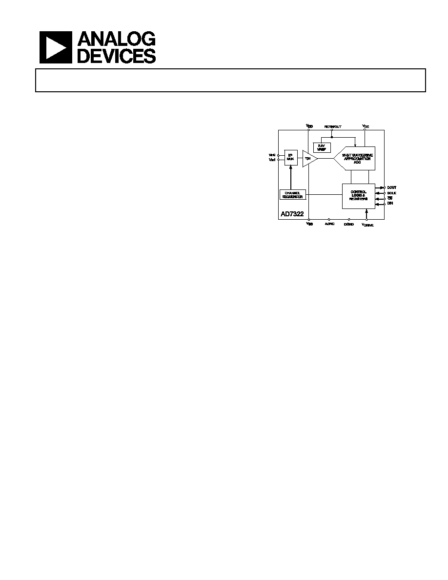
GENERAL DESCRIPTION
The AD7322 is a 2-Channel, 12-Bit Plus Sign, 1 MSPS
Successive Approximation ADC. The ADC has a high speed
serial interface that can operate at throughput rates up to 1
MSPS.
The AD7322 can handle True Bipolar Analog input signals. The
Bipolar ranges are software selectable by programming the on
board Range Register. Bipolar input ranges include ± 10V, ± 5V,
± 2.5V. The AD7322 can also handle a 0 to 10 V uniploar input
range, which is also software selectable. Each analog input
channel can be independently programmed to one of the input
ranges by setting the appropriate bits in the Range Register.
The Analog Input Channels can be configured as Single-Ended,
Fully Differential or Pseudo Differential. Dedicated Control
Register bits are used to configure the Analog inputs. The
AD7322 contains a Channel Sequencer, allowing automatic
conversions between each analog input channel.
The ADC contains a 2.5V Internal reference. The AD7322 also
allows for external Reference operation. If a 3V external
reference is applied to the REFIN/OUT pin, the ADC can
handle a True Bipolar ± 12 V Analog input range. Minimum
V
DD
and V
SS
supplies of ± 12V are required for this ± 12 V input
range.
* Patent Pending
FUNCTIONAL BLOCK DIAGRAM
Figure 1.
The Serial clock frequency, SCLK, applied to the ADC will
determine the maximum throughput rate the ADC can operate
at. The SCLK signal is used as the conversion clock and also to
transfer data to and from the ADC. The Serial interface is
SPI
TM
, QSPI
TM
, MICROWIRE
TM
and DSP compatible.
The AD7322 offers power down modes to reduce the power
consumption of the ADC at lower throughput rates.
PRODUCT HIGHLIGHTS
1. The AD7322 can accept True Bipolar Analog Input signals,
±10V, ±5V, ±2.5V and 0 to 10V unipolar signals.
2. The Two Analog Inputs can be configured as Two Single-
Ended inputs, One True Differential or One Pseudo Differential
Input. The AD7322 has high Impedance Analog Inputs.
3. The AD7322 features a High Speed Serial Interface.
Throughput Rates up to 1 MSPS can be achieved on the
AD7322.
4. Low Power, 12 mW at maximum throughput rate of 1 MSPS.
Information furnished by Analog Devices is believed to be accurate and reliable.
However, no responsibility is assumed by Analog Devices for its use, nor for any
infringements of patents or other rights of third parties that may result from its use.
Specifications subject to change without notice. No license is granted by implication
or otherwise under any patent or patent rights of Analog Devices. Trademarks and
registered trademarks are the property of their respective companies.
One Technology Way, P.O. Box 9106, Norwood, MA 02062-9106, U.S.A.
Tel: 781.329.4700
www.analog.com
Fax: 781.326.8703
© 2004 Analog Devices, Inc. All rights reserved.
Rev. PrE

AD7322
Preliminary Technical Data
TABLE OF CONTENTS
AD7322--Specifications.................................................................. 3
Absolute Maximum Ratings............................................................ 6
Pin Functional Descriptions ....................................................... 7
Terminology ...................................................................................... 8
Theory of Operation.....................................................................9
AD7322 Registers ........................................................................... 12
Serial interface ................................................................................ 17
OUTLINE DIMENSIONS
.................................................................. 18
REVISION HISTORY
Revision PrE: Preliminary Version
Rev. PrE | Page 2 of 18
AD7322
Preliminary Technical Data
AD7322--SPECIFICATIONS
1
Table 1. Unless otherwise noted, V
DD
= + 4.75V to +16.5V, V
SS
= -4.75V to 16.5V, V
CC
= 2.7V to 5.25V, V
DRIVE
= 2.7V to 5.25V, V
REF
= 2.5V Internal/External, f
SCLK
= 20 MHz, f
S
= 1 MSPS T
A
= T
MAX
to T
MIN
Parameter Specification
Units Test
Conditions/Comments
DYNAMIC PERFORMANCE
F
IN
= 50 kHz Sine Wave
Signal to Noise Ratio (SNR)
2
78
dB min
Differential Mode
75
dB min
Single-Ended /Pseudo Differential Mode
Signal to Noise + Distortion (SINAD)
2
77
dB min
Differential Mode
74
dB min
Single-Ended/Pseudo Differential Mode
Total Harmonic Distortion (THD)
2
-TBD dB
max
Peak Harmonic or Spurious Noise
(SFDR)
2
-TBD
dB max
Intermodulation Distortion (IMD)
2
F
a
= 40.1 kHz, F
b
= 41.5 kHz
Second Order Terms
-88
dB typ
Third Order Terms
-88 dB
typ
Aperature Delay
2
10 ns
max
Aperature Jitter
2
50 ps
typ
Common Mode Rejection (CMRR)
2
TBD dB
typ
Channel-to-Channel Isolation
2
-80 dB
typ
F
IN
= 400 kHz
Full Power Bandwidth
2
13
1.5
MHz typ
MHz typ
@ 3 dB
@ 0.1 dB
DC ACCURACY
Resolution 12+Sign
Bits
Integral Nonlinearity
2
±1.5 LSB
max
Differential Nonlinearity
2
± 0.95
LSB max
Guaranteed No Missing Codes to 13-Bits
Offset Error
3
±6
LSB max
Unipolar Range with Straight Binary output coding
Offset Error Match
2
±0.5
LSB
max
Gain Error
2
±2 LSB
max
Gain Error Match
2
±0.6 LSB
max
Positive Full-Scale Error
2
±2
LSB max
Bipolar Range with Twos Complement Output Coding
Positive Full Scale Error Match
2
±0.6 LSB
max
Bipolar Zero Error
2
±6 LSB
max
Bipolar Zero Error Match
2
±0.5 LSB
max
Negative Full Scale Error
2
±2
LSB max
Negative Full Scale Error Match
2
±0.5 LSB
max
ANALOG INPUT
Input Voltage Ranges
(Programmed via Range Register)
±10V
±5V
±2.5V
0 to 10V
Volts V
DD
= +10V min , V
SS
= -10V min, V
CC
= 2.7V to 5.25V
V
DD
= +5V min, V
SS
= -5V min, V
CC
= 2.7V to 5.25V
V
DD
= +5V min, V
SS
= - 5V min, V
CC
= 2.7V to 5.25V
V
DD
= +10V min, V
SS
= 0 V min, V
CC
= 2.7V to 5.25V
DC Leakage Current
±10
nA max
Input Capacitance
8
pF typ
When in Track, ±10V Range
11
pF typ
When in Track, ±5V, 0 to 10V Range
19
pF typ
When in Track, ±2.5V Range
6
pF typ
When in Hold
REFERENCE INPUT/OUTPUT
Input Voltage Range
+2.5 to +3V
V min to
max
Input DC Leakage Current
±1
µA max
Input Capactiance
20
pF typ
Reference Output Voltage
2.49/2.51
Vmin/max
Reference Temperature Coefficient
25
ppm/°C
max
Rev. PrE | Page 3 of 18

AD7322
Preliminary Technical Data
Parameter Specification
Units Test
Conditions/Comments
Reference Output Impedance
25
typ
LOGIC INPUTS
Input High Voltage, V
INH
0.7*V
DRIVE
V
min
Input High Voltage, V
INL
0.3*V
DRIVE
V
max
Input Current, I
IN
± 1
µA max
V
IN
= 0V or V
CC
Input Capacitance, C
IN
3
10
pF max
LOGIC OUTPUTS
Output High Voltage, V
OH
V
DRIVE
- 0.2V
V min
I
SOURCE
= 200 µA
Output Low Voltage, V
OL
0.4
V
max
I
SINK
= 200 µA
Floating State Leakage Current
±1
µA max
Floating State Output Capacitance
3
10 pF
max
Output Coding
Straight
Natural
Binary
Coding bit set to 1 in Control Register
Two's
Complement
Coding bit set to 0 in Control Register
CONVERSION RATE
Conversion Time
800
ns max
16 SCLK Cycles with SCLK = 20 MHz
Track-and-Hold Acquisition Time
150
ns max
Sine Wave Input
150
ns max
Full Scale Step input
Throughput Rate
1
MSPS max
See Serial Interface section
POWER REQUIREMENTS
Digital Inputs = 0V or V
CC
V
DD
4.75V/+16.5V
V
min/max
See
V
SS
-4.75V/16.5V
V
min/max
See
V
CC
2.7V / 5.25V
V min/max
See
Normal Mode
I
DD
200
µA
max
I
SS
200
µA
max
I
CC
2
mA
max
Auto-Standby Mode
F
SAMPLE
= TBD
I
DD
TBD
µA
max
I
SS
TBD
µA
max
I
CC
1.6
mA
typ
Auto-Standby Mode
F
SAMPLE
= TBD
I
DD
TBD
µA
max
I
SS
TBD
µA
max
I
CC
1
mA
typ
Full Shutdown Mode
I
DD
TBD
µA
max
I
SS
TBD
µA
max
I
CC
1
µA max
SCLK On or Off
POWER DISSIPATION
Normal Mode
12
mW max
V
DD
= +5V, V
SS
= -5V, V
CC
= 5V,
Table 5
Table 5
Table 5
NOTES
1
Temperature ranges as follows: -40°C to +85°C
2
See Terminology
3
Guaranteed by Characterization
Specifications subject to change without notice.
Rev. PrE | Page 4 of 18

AD7322
Preliminary Technical Data
TIMING SPECIFICATIONS
Table 2. Unless otherwise noted,
V
DD
= +4.75V to + 16.5V, V
SS
= -4.75 to 16.5V, V
CC
=2.7V to 5.25, V
DRIVE
=2.7V to 5.25, V
REF
=
2.5V Internal/External, T
A
= T
MAX
to T
MIN
Parameter
Limit at T
MIN
, T
MAX
Unit Description
f
SCLK
10 kHz
min
20
MHz
max
t
CONVERT
16×t
SCLK
ns
max
T
SCLK
= 1/f
SCLK
t
QUIET
50
ns
max
Minimum Time between End of Serial Read and Next Falling Edge of CS
t
1
10
ns
min
Minimum CS Pulse width
t
2
10 ns
min
CS to SCLK Setup Time
t
3
20 ns
max
Delay from CS until D
OUT
Three-State Disabled
t
4
TBD
ns max
Data Access Time after SCLK Falling Edge.
t
5
0.4t
SCLK
ns min
SCLK Low Pulsewidth
t
6
0.4t
SCLK
ns min
SCLK High Pulsewidth
t
7
10
ns min
SCLK to Data Valid Hold Time
t
8
25
ns max
SCLK Falling Edge to D
OUT
High Impedance
10
ns min
SCLK Falling Edge to D
OUT
High Impedance
t
9
TBD
ns min
DIN set-up time prior to SCLK falling edge
t
10
5
ns min
DIN hold time after SCLK falling edge
1
µs max
Power up from Auto Standby
TBD
µs max
Power up from Full Shutdown/Auto Shutdown Mode
Figure 2. Serial Interface timing Diagram
Rev. PrE | Page 5 of 18
AD7322
Preliminary Technical Data
ABSOLUTE MAXIMUM RATINGS
Table 3. T
A
= 25°C, unless otherwise noted
V
DD
to AGND, DGND
-0.3 V to +17.5 V
V
SS
to AGND, DGND
+0.3 V to 17.5 V
V
CC
to AGND, DGND
-0.3V to +7V
V
DRIVE
to V
CC
-0.3 V to V
CC
+ 0.3V
V
DRIVE
to AGND, DGND
-0.3 V to +7V
AGND to DGND
-0.3 V to +0.3 V
Analog Input Voltage to AGND
TBD
Digital Input Voltage to DGND
-0.3 V to +7 V
Digital Output Voltage to GND
-0.3 V to V
DRIVE
+0.3V
REF
IN
to AGND
-0.3 V to V
CC
+0.3V
Input Current to Any Pin Except Supplies
2
±10mA
Operating Temperature Range
-40°C to +85°C
Storage Temperature Range
-65°C to +150°C
Junction Temperature
+150°C
TSSOP Package
JA
Thermal Impedance
143 °C/W
JC
Thermal Impedance
45 °C/W
Lead Temperature, Soldering
Reflow (10 30 sec)
+235(-0/+5)°C
ESD TBD
Rev. PrE | Page 6 of 18

AD7322
Preliminary Technical Data
Pin Functional Descriptions
14
13
12
11
9
TOP VIEW
(Not to
Scale)
8
1
2
3
4
7
6
5
AD7322
CS
DIN
SCLK
REFIN/OUT
VSS
DGND
DOUT
VIN1
10
VDRIVE
VIN0
AGND
DGND
VDD
8++
Figure 3. AD7322 Pin Configuration TSSOP
Table 4. AD7324 Pin Function Descriptions
Pin
Mnemonic
Pin
Number
Description
SCLK 14 Serial Clock. Logic Input. A serial clock input provides the SCLK used for accessing the data
from the AD7322. This clock is also used as the clock source for the conversion process.
D
OUT
12 Serial Data Output. The conversion output data is supplied to this pin as a serial data stream.
The bits are clocked out on the falling edge of the SCLK input and 16 SCLKs are required to
access the data. The data stream consists of two leading zeros, one channel identification bit, a
Sign bit followed by 12 bits of conversion data. The data is provided MSB first. See the Serial
Interface section.
CS
1
Chip Select. Active low logic input. This input provides the dual function of initiating
conversions on the AD7322 and frames the serial data transfer.
DIN 2 Data In. Data to be written to the on-chip registers is provided on this input and is clocked into
the register on the falling edge of SCLK. See Register section.
AGND 4
Analog Ground. Ground reference point for all analog circuitry on the AD7322. All analog input
signals and any external reference signal should be referred to this AGND voltage.
REF
IN/
REF
OUT
5
Reference Input/ Reference Output pin. When enabled the on-chip reference is available on
this pin for use external to the AD7322. Alternativley, the internal reference can be disabled
and an external reference applied to this input. When using the AD7322 with an external
reference, the internal reference must be disabled via the control register. The nominal
reference voltage is 2.5 V, which appears at the pin. The default on power up is for external
Reference operation. See
.
V
CC
10 Analog Supply Voltage, 2.7 V to 5.25 V. This is the supply voltage for the ADC core on the
AD7322. This supply should be decoupled to AGND.
V
DD
9
Positive power supply voltage. This is the positive supply voltage for the Analog Input section.
V
SS
6 Negative power supply voltage. This is the negavtive supply voltage for the Analog Input
section.
DGND
3,13
This is the Digital Ground pin.
V
DRIVE
11 Logic Power Supply input. The voltage applied to this pin determines the operating voltge of
the sertial inteface.
Vin0-Vin1 7,8
Analog input 0 through Analog Input 1. The analog inputs are multiplexed into the on-chip
track-and-hold. The analog input channel for conversion is selected by programming the
channel address bit ADD0, in the control register. The inputs can be configured as 2 Single-
Ended Inputs, 1 True Differential Input pair, 1 Pseudo Differential inputs. The configuration of
the Analog inputs is selected by programming the Mode bits, Mode1 and Mode0, in the
Control Register. The input range on each input channel is controlled by programming the
range register. Inputs ranges of ±10V, ±5V, ±2.5V and 0 to 10V can be selected on each analog
input channel. See Register section.
Table 8
Rev. PrE | Page 7 of 18

AD7322
Preliminary Technical Data
TERMINOLOGY
Differential Nonlinearity
This is the difference between the measured and the ideal 1 LSB
change between any two adjacent codes in the ADC.
Integral Nonlinearity
This is the maximum deviation from a straight line passing
through the endpoints of the ADC transfer function. The
endpoints of the transfer function are zero scale, a point 1 LSB
below the first code transition, and full scale, a point 1 LSB
above the last code transition.
Offset Code Error
This applies to Straight Binary output coding. It is the deviation
of the first code transition (00 . . . 000) to (00 . . . 001) from the
ideal, i.e., AGND + 1 LSB.
Offset Error Match
This is the difference in Offset Error between any two input
channels.
Gain Error
This applies to Straight Binary output coding. It is the deviation
of the last code transition (111 . . . 110) to (111 . . . 111) from the
ideal (i.e., 4 x VRef 1 LSB, 2 x V
REF
1 LSB, V
REF
1 LSB) after
the offset error has been adjusted out.
Gain Error Match
This is the difference in Gain Error between any two input
channels channels.
Bipolar Zero Code Error
This applies when using twos complement output coding and a
bipolar Analog Input. It is the deviation of the midscale
transition (all 1s to all 0s) from the ideal V
IN
voltage, i.e., AGND
- 1 LSB.
Bipolar Zero Code Error Match
This refers to the difference in Bipolar Zero Code Error
between any two input channels.
Positive Full Scale Error
This applies when using twos complement output coding and
any of the bipolar Analog Input ranges. It is the deviation of the
last code transition (011...110) to (011...111) from the ideal (
+4 x V
REF
- 1 LSB, + 2 x V
REF
1 LSB, + V
REF
1 LSB) after the
bipolar Zero Code Error has been adjusted out.
Positive Full Scale Error Match
This is the difference in Positive Full Scale error between any
two input channels.
Negative Full Scale Error
This applies when using twos complement output coding and
any of the bipolar Analog Input ranges. This is the deviation of
the first code transition (10...000) to (10...001) from the ideal
(i.e., - 4 x V
REF
+ 1 LSB, - 2 x V
REF
+ 1 LSB, - V
REF
+ 1 LSB) after
the Bipolar Zero Code Error has been adjusted out.
Negative Full Scale Error Match
This is the difference in Negative Full Scale error between any
two input channels.
Track-and-Hold Acquisition Time
The track-and-hold amplifier returns into track mode after the
fifteenth SCLK falling edge. Track-and-hold acquisition time is
the time required for the output of the track-and-hold amplifier
to reach its final value, within ±1/2 LSB, after the end of
conversion.
Signal to (Noise + Distortion) Ratio
This is the measured ratio of signal to (noise + distortion) at the
output of the A/D converter. The signal is the rms amplitude of
the fundamental. Noise is the sum of all non-fundamental
signals up to half the sampling frequency (f
S
/2), excluding dc.
The ratio is dependent on the number of quantization levels in
the digitization process; the more levels, the smaller the
quantization noise. The theoretical signal to (noise + distortion)
ratio for an ideal N-bit converter with a sine wave input is given
by:
Signal to (Noise + Distortion) = (6.02N + 1.76) dB
Thus for a 13-bit converter, this is 80.02 dB.
Total Harmonic Distortion
Total harmonic distortion (THD) is the ratio of the rms sum of
harmonics to the fundamental. For the AD7322 it is defined as:
1
2
6
2
5
2
4
2
3
2
2
log
20
)
(
V
V
V
V
V
V
dB
THD
+
+
+
+
=
where V
1
is the rms amplitude of the fundamental and V
2
, V
3
,
V
4
, V
5
and V
6
are the rms amplitudes of the second through the
sixth harmonics.
Peak Harmonic or Spurious Noise
Peak harmonic or spurious noise is defined as the ratio of the
rms value of the next largest component in the ADC output
spectrum (up to fS/2 and excluding dc) to the rms value of the
fundamental. Normally, the value of this specification is
determined by the largest harmonic in the spectrum, but for
ADCs where the harmonics are buried in the noise floor, it will
be a noise peak.
Channel-to-Channel Isolation
Channel-to-channel isolation is a measure of the level of
crosstalk between any two channels. It is measured by applying
a full-scale, 400 kHz sine wave signal to all unselected input
channels and determining how much that signal is attenuated in
Rev. PrE | Page 8 of 18

Preliminary Technical Data
AD7322
the selected channel with a 50 kHz signal. The figure given is
the worst-case across all eight channels for the AD7322.
Intermodulation Distortion
With inputs consisting of sine waves at two frequencies, fa and
fb, any active device with non-linearities will create distortion
products at sum and difference frequencies of mfa ± nfb where
m, n = 0, 1, 2, 3, etc. Intermodulation distortion terms are those
for which neither m nor n are equal to zero. For example, the
second order terms include (fa + fb) and (fa fb), while the
third order terms include (2fa + fb), (2fa fb), (fa + 2fb) and (fa
2fb).
The AD7322 is tested using the CCIF standard where two input
frequencies near the top end of the input bandwidth are used.
In this case, the second order terms are usually distanced in
frequency from the original sine waves while the third order
terms are usually at a frequency close to the input frequencies.
As a result, the second and third order terms are specified
separately. The calculation of the intermodulation distortion is
as per the THD specification where it is the ratio of the rms
sum of the individual distortion products to the rms amplitude
of the sum of the fundamentals expressed in dBs.
PSR (Power Supply Rejection)
Variations in power supply will affect the full-scale transition
but not the converter's linearity. Power supply rejection is the
maximum change in full-scale transition point due to a change
in power supply voltage from the nominal value. See Typical
Performance Curves.
Theory of Operation
CIRCUIT INFORMATION
The AD7322 is a fast, 2-Channel, 12-bit plus Sign, Bipolar Input,
Serial A/D converter. The AD7322 can accept bipolar input
ranges that include ±10V, ±5V, ±2.5V, it can also accept 0 to 10V
unipolar input range. Different Analog input ranges can be
programmed on each analog input Channel via the on-chip
range register. The AD7322 has a high speed serial interface that
can operate at throughput rates up to 1 MSPS.
The AD7322 requires V
DD
and V
SS
dual
supplies for the high
voltage Analog input structure. These supplies must be equal to
or greater than the Analog input range. See
for the
minimum requirements on these supplies for each Analog Input
Range. The AD7322 requires a low voltage 2.7V to 5.25 V V
CC
supply to power the ADC core.
Table 5
Table 5. Reference and Supply Requirements for each Analog
Input Range
Ain Range
V
DD
/V
SS
Min
V
CC
Reference
V
± 12 V
± 12 V
3 V to 5V
3V
± 10 V
± 10V
3 V to 5 V
2.5 V
± 5 V
± 5 V
3V to 5V
2.5 V
± 2.5 V
± 5 V
3 V to 5 V
2.5 V
0 to 10 V
± 10 V
3 V to 5 V
2.5 V
The Analog Inputs can be configured as either 2 Single-Ended
inputs, 1 True Differential Inputs, or 1 Pseudo Differential
Input. Selection can be made by programming the Mode bits,
Mode0 and Mode1, in the on-chip Control Register.
The serial clock input accesses data from the part but also
provides the clock source for each successive approximation
ADC. The AD7322 has an on-chip 2.5 V reference. If an
External Reference is the preferred option the user must write
to the reference bit in the control register to disable the internal
Reference.
The AD7322 also features power-down options to allow power
saving between conversions. The power-down modes are
selected by programming the power management bits in the on-
chip Control Register, as described in the Modes of Operation
section.
CONVERTER OPERATION
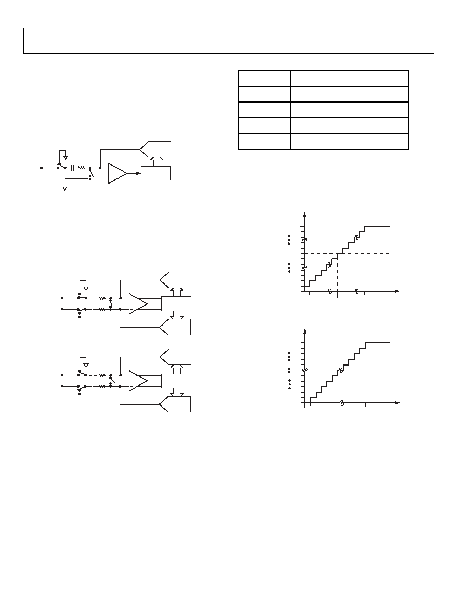
The AD7322 is a successive approximation analog-to-digital
converter, based around two capacitive DACs. F
and
show simplified schematics of the ADCs in Single
Ended Mode during the acquisition and conversion phase,
respectively.
and Fi
show simplified schematics
of the ADC in Differential Mode during acquisition and
conversion phase, respectively. The ADC is comprised of
control logic, a SAR, and a capacitive DAC. In F
(the
acquisition phase), SW2 is closed and SW1 is in position A, the
comparator is held in a balanced condition, and the sampling
capacitor array acquires the signal on the input.
igure 4
igure 4
Figure 4. ADC Acquisition Phase(Single Ended)
Figure 5
Figure 6
gure 7
Vin0
AGND
CONTROL
LOGIC
CAPACITIVE
DAC
SW2
SW1
CS
A
B
COMPARATOR
Rev. PrE | Page 9 of 18
AD7322
Preliminary Technical Data
When the ADC starts a conversion (
), SW2 will open
and SW1 will move to position B, causing the comparator to
become unbalanced. The control logic and the charge
redistribution DAC is used to add and subtract fixed amounts
of charge from the sampling capacitor arrays to bring the
comparator back into a balanced condition. When the
comparator is rebalanced, the conversion is complete. The
Control Logic generates the ADC output code.
Figure 5
Figure 5. ADC Conversion Phase(Single Ended)
Vin0
AGND
CONTROL
LOGIC
CAPACITIVE
DAC
SW2
SW1
CS
A
B
COMPARATOR
Figure 6
Figure 6. ADC Differential Configuration during Acquisition Phase
Vin+
VREF
CONTROL
LOGIC
CAPACITIVE
DAC
SW3
SW1
CS
A
B
COMPARATOR
CAPACITIVE
DAC
SW2
CS
A
B
Vin-
shows the differential configuration during the
Acquisition phase. For the Conversion Phase, SW3 will open,
SW1 and SW2 will move to position B, see
. The output
impedances of the source driving the Vin+ and Vin- pins must
be matched; otherwise the two inputs will have different settling
times, resulting in errors.
Figure 7
Figure 7. ADC Differential Configuration during Conversion Phase
Vin+
VREF
CONTROL
LOGIC
CAPACITIVE
DAC
SW3
SW1
CS
A
B
COMPARATOR
CAPACITIVE
DAC
SW2
CS
A
B
Vin-
Output Coding
The AD7322 default output coding is set to two's complement.
The output coding is controlled by the Coding bit in the
Control Register. To change the output coding to Straight
Binary Coding the Coding bit in the Control Register must be
set. When operating in Sequence mode the output coding for
each channel in the sequence will be the value written to the
coding bit during the last write to the Control Register.
Transfer Functions
The designed code transitions occur at successive integer LSB
values (i.e., 1 LSB, 2 LSB, and so on). The LSB size is dependant
on the Analog input Range selected.
Table 6. LSB sizes for each Analog Input Range
Input Range
Full Scale Range/4096
LSB Size
±10V 20V/4096
4.882
mV
±5V 10V/4096
2.441
mV
±2.5V 5V/4096
1.22
mV
0 to 10V
10V/4096
2.441 mV
The ideal transfer characteristic for the AD7322 when Twos
Complement coding is selected is shown in
, and the
ideal transfer characteristic for the AD7322 when Straight
Binary coding is selected is shown in
.
Figure 8
Figure 8. Twos Complement Transfer Characteristic (Bipolar Ranges)
Figure 9
Figure 9. Straight Binary Transfer Characteristic (Bipolar Ranges)
000...000
-
FSR/2 + 1LSB
A
D
C CODE
ANALOG INPUT
011...111
100...001
100...010
011...110
000...001
111...111
+FSR/2 - 1LSB
100...000
VREF - 1LSB
000...000
-FSR/2
A
DC CODE
ANALOG INPUT
111...111
000...001
000...010
111...110
111...000
011...111
1LSB
FSR/2 -1LSB
ANALOG INPUT
The analog inputs of the AD7322 may be configured as Single-
Ended, True differential or Pseudo Differential via the Control
Register Mode Bits as shown in
of the Register Section.
The AD7322 can accept True bipolar input signals. On power
up the Analog inputs will operate as 2 Single-Ended Analog
Input Channels. If True Differential or Pseudo Differential is
required, a write to the Control register is necessary to change
this configuration after power up.
Table 9
Figure 10 shows the equivalent Analog input circuit of the
AD7322 in Single-Ended Mode.
shows the equivalent
Analog input structure in Differential mode. The Two Diodes
provide ESD protection for the Analog Inputs.
Figure 11
Rev. PrE | Page 10 of 18
Preliminary Technical Data
AD7322
D
D
VDD
C2
R1
Vin0
VSS
C1
Figure 10. Equivalent Analog Input Circuit-(Single Ended)
Figure 10
D
D
VDD
C2
R1
Vin+
VSS
C1
D
D
VDD
C2
R1
Vin-
VSS
C1
Figure 11. Equivalent Analog Input Circuit-(Differential)
Figure 11
Care should be taken to ensure the Analog Input never exceeds
the V
DD
and V
SS
supply rails by more than 300 mV. This will
cause the diodes to become forward biased and start
conducting into either the V
DD
or V
SS
rails. These diodes can
conduct up to 10 mA without causing irreversible damage to
the part.
The Capacitor C1, in
and
is typically 4 pF
and can primarily be attributed to pin capacitance. The resistor
R1, is a lumped component made up of the on-resistance of the
input multiplexer and the track-and-hold switch. The Capacitor
C2, is the sampling capacitor, its capacitance will vary
depending on the Analog input range selected.
Track-and-Hold Section
The Track-and-Hold on the Analog Input of the AD7322 allows
the ADC to accurately convert an input sine wave of full scale
amplitude to 13-Bit accuracy. The input bandwidth of the
Track-and-Hold is greater than the Nyquist rate of the ADC ,
the AD7322 can handle frequencies up to 13 MHz.
The Track-and-Hold enters its tracking mode on the 15
th
SCLK
falling edge after the CS falling edge. The time required to
acquire an input signal will depend on how quickly the
sampling capacitor is charged. With zero source impedance 300
ns will be sufficient to acquire the signal to the 13-bit level.
The acquisition time required is calculated using the following
formula:
t
ACQ
= 10 x ((R
SOURCE
+ R) C)
where C is the Sampling Capacitance and R is the resistance
seen by the track-and-hold amplifier looking back on the input.
For the AD7322, the value of R will include the on-resistance of
the input multiplexer. The value of R is typically 300 . R
SOURCE
should include any extra source impedance on the Analog
input.
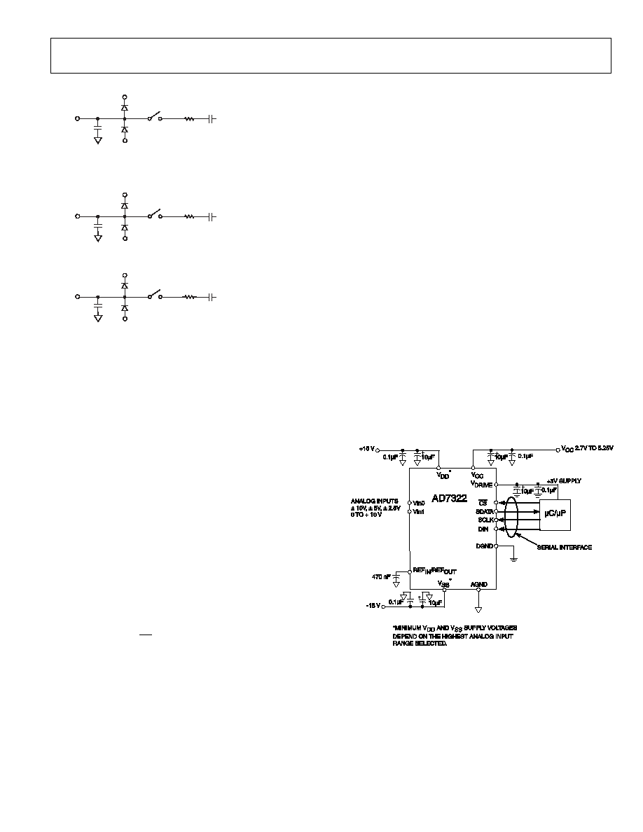
TYPICAL CONNECTION DIAGRAM
Figure 12
Figure 12
Figure 12. Typical Connection Diagram
shows a typical connection diagram for the AD7322.
In this configuration the AGND pin is connected to the Analog
ground plane of the system. The DGND pin is connected to the
Digital ground plane of the system. The Analog Inputs on the
AD7322 can be configured to operate in Single Ended, True
Differential or Pseudo Differential Mode. The AD7322 can
operate with either the internal or an external reference. In
, the AD7322 is configured to operate with the internal
2.5V reference. A 470 nF decoupling capacitor is required when
operating with the internal reference.
The V
CC
pin can be connected to either a 3V or a 5V supply
voltage. The V
DD
and V
SS
are the dual supplies for the high
voltage analog input structures. The voltage on these pins must
be equal to or greater than the highest analog input range
selected on the analog input channels, see
for more
information. The V
DRIVE
pin is connected to the supply voltage
of the microprocessor. The voltage applied to the V
DRIVE
input
controls the voltage at which the serial interface operates.
Table 5
Rev. PrE | Page 11 of 18
AD7322
Preliminary Technical Data
AD7322 REGISTERS
The AD7322 has two-programmable registers, the Control Register and the Range Register. These registers are write only registers.
Addressing these Registers
A serial transfer on the AD7322 consists of 16 SCLK cycles. The three MSBs on the DIN line during each 16 SCLK transfer are decoded to
determine which register is addressed. The three MSBs consists of the Write bit, ZERO bit and a Register Select bit. The Register Select bit
is used to determine which of the Two on-board registers is selected. The Write bit will determine if the Data on the DIN line following
the Register select bit is loaded into the addressed register or not. If the Write bit is 1 the bits will be loaded into the register addressed by
the Register Select bit. If the Write Bit is a 0 the data on the DIN will not be loaded into any register and both registers will remain
unchanged.
Table 7. Decoding Register Select bit and Write bit.
Write
ZERO
Register Select2
Comment
0
0
0
Data on the DIN line during this serial transfer will be ignored. Register contents will
remain unchanged.
1
0
0
This combination selects the Control Register. The subsequent 12 bits will be loaded into
the Control Register.
1
0
1
This combination selects the Range Register. The subsequent 8 bits will be loaded into
the Range Register.
CONTROL REGISTER
The Control Register is used to select the Analog Input configuration, Reference, Coding, Power mode etc. The Control Register is a write
only 12-bit register. Data loaded on the DIN line corresponds to the AD7322 configuration for the next conversion. Data should be
loaded into the Control Register after the Range Register has been initialized. The bit functions of the Control Register are outlined in
.
Table 8
Table 8. Control Register
Control Register (The Power-up status of all bits is 0)
MSB
DB14
DB13 DB12 DB11 DB10 DB9 DB8 DB7 DB6 DB5 DB4 DB3 DB2 DB1
Write
ZERO
Register
Select
ZERO ZERO ADD0 Mode1 Mode0 PM1 PM0 Coding Ref Seq1 Seq2 ZERO
Bit Mnemonic
Comment
10 ADD0 ThIs Channel Address bit is used to select the analog input channel for the next conversion if the Sequencer is
not being used.
9, 8
Mode1,
Mode0
These two mode bits are used to select the configuation on the two analog Input Pins. They are used in
conjunction with the channel Address bit. On the AD7322 the analog inputs can be configured as either 2
Single Ended Inputs, 1 Fully Differential Input, 1 Pseudo Differential input. See
.
7,6 PM1,
PM0
Power Management Bits. These two bits are used to select different power mode options on the AD7322. See
.
5 Coding
This bit is used to select the type of output coding the AD7322 will use for the next conversion result. If the
Coding = 0 then the output coding will be 2s Complement. If Coding = 1, then the output coding will be
Straight Binary. When operating in Sequence mode the output coding for each channel will be the value
written to the coding bit during the last write to the Control Register.
4 Ref Reference bit. This bit is used to enable or disable the internal reference. If this Ref = 0 then the Internal
Reference will be enable and used for the next conversion. If ref = 1 then an external Reference will be used
for the next conversion and the internal reference will be disabled. When operating in Sequence mode the
Table 9
Table 10
Rev. PrE | Page 12 of 18

Preliminary Technical Data
AD7322
Reference used for each channel will be the value written to the Ref bit during the last write to the Control
Register.
3,2
Seq1/Seq2
The Sequence 1 and Sequence 2 bits are used to control the operation of the Sequencer. See Table 8
14,12,11,1
ZERO
A zero must be written to this bit to ensure correct operation of the AD7322.
Table 9. Analog Input Configuration Selection
Channel Address Bit
Mode1 =1, Mode0 = 1
Mode1 = 1, Mode0 =0
Mode1 = 0, Mode0 =1
Mode1 =0, Mode0 =0
1 Pseudo Differential I/p
1Fully Differential i/p
Not Allowed
Two-Single Ended i/ps
ADD0 Vin+
Vin-
Vin+ Vin-
Vin+
Vin-
0 Vin0 Vin1
Vin0
Vin1
Vin0 AGND
1 Vin0 Vin1
Vin0
Vin1
Vin1 AGND
Table 10. Power Mode Selection
PM1 PM0 Description
1 1
Full Shutdown Mode,
In this mode all internal circuitry on the
AD7322 is powered down. Information in the Control register is
retained when the AD7322 is in Full Shutdown Mode.
1 0
Auto Shutdown Mode,
The AD7322 will enter Full Shut down
at the end of each conversion when the control register is
updated. All internal circuitry is powered down in Full
Shutdown.
0 1
Auto Standby Mode,
In this mode all internal circuitry is
powered down excluding the internal Reference. The AD7322
will enter Auto Standby Mode at the end of the Conversion after
the control register is updated.
0 0
Normal
Mode,
All internal Circuitry is powered up at all times.
Table 11. Sequencer Selection
Seq1 Seq2 Sequence
type
0
0
The Channel Sequencer is not used. The Analog Channel selected by programming the ADD0 bit in the
Control Register selects the next channel for conversion.
1
0
This Configuration is used in conjunction with the Channel Address Bit in the Control Register. Provided that
the channel Address bit is 1, the ADC will convert firstly on channel 0 then channel 1 and will repeat this
sequence until the Seq bits are changed in the Control Register.
1
1
The Channel Sequencer is not used. The Analog Channel selected by programming the ADD0 bit in the
Control Register selects the next channel for conversion.
Rev. PrE | Page 13 of 18
AD7322
Preliminary Technical Data
RANGE REGISTER
The Range register to used to select one Analog input Range per Analog input channel. It is a 4-Bit write only Register, with two dedicated
Range bits for each of the two Analog Input Channels. There are four Analog input Ranges to choose from, ±10V, ±5V, ±2.5V, 0 to 10V. A
write to the Range Register is selected by setting the Write bit to 1 and the Register Select bit to 1. Once the initial write to the Range
Register occurs the AD7322 automatically configures the two Analog inputs to the appropriate range, as indicated by the Range register,
each time any one of these analog input channels is selected. The ±10V input Range is selected by default on each analog input channel.
See
.
Table 12
Table 12. Range Register
Write
Register
Select 1
Register
Select 2
Vin0A Vin0B Vin1A Vin1B
VinXA VinXB Description
0
0
This combination selects the ± 10V
Input Range on Analog Input X.
0
1
This combination selects the ±5V Input
Range on Analog Input X.
1
0
This combination selects the ± 2.5V
Input Range on Analog Input X.
1
1
This combination selects the 0 to 10V
Input Range on Analog Input X.
Rev. PrE | Page 14 of 18

AD7322
Preliminary Technical Data
REFERENCE
The AD7322 can operate with either the internal 2.5V on-chip
reference or an externally applied reference. The internal
reference is selected by setting the REF bit in the Control
Register to 1. On power up the REF bit will be 0, selecting the
external Reference for the AD7322 conversion. For external
reference operation the REF
IN
/REF
OUT
pin should be decoupled
to AGND with a 470 nF capacitor.
The internal Reference circuitry consists of a 2.5V band gap
reference and a reference buffer. When operating the AD7322 in
internal Reference mode the 2.5V internal reference is available
at the REF
IN
/REF
OUT
pin. When using the AD7322 with the
internal reference the REFIN/REFOUT pin should be
decoupled to AGND using a 0.47 µF cap. It is recommended
that the Internal Reference be buffered before applying it else
where in the system.
The AD7322 is specified for a 2.5V to 3V reference range. When
a 3V reference is selected the ranges will be, ±12V, ±6V, ±3V
and 0 to 12V. For these ranges the V
DD
and V
SS
supply must be
equal to or greater than the max Analog Input Range selected.
On power up if the internal reference operation is required for
the ADC conversion, a write to the control register is necessary
to set the REF bit to 1. During the Control Register write the
conversion result from the first initial conversion will be invalid.
The reference buffer will require TBD us to power up and
charge the 0.47 µF decoupling cap, during the power up time
the conversion result from the ADC will be invalid.
Rev. PrE | Page 15 of 18

AD7322
Preliminary Technical Data
MODES OF OPERATION
The AD7322 has a number of different modes of operation.
These modes are designed to provide flexible power
management options. These options can be chosen to optimize
the power dissipation/throughput rate ratio for the differing
application requirements. The mode of operation of the
AD7322 is controlled by the Power Management bits, PM1 and
PM0, in the Control register as detailed in
.The default
mode is Normal Mode, where all internal circuitry is fully
powered up.
Table 10
Normal Mode (PM1 = PM0 = 0)
This mode is intended for the fastest throughput rate
performance, the AD7322 is fully powered up at all times.
shows the general diagram of operation of the
AD7322 in Normal Mode.
Figure 13
Figure 13. Normal Mode
The Conversion is initiated on the falling edge of CS and the
track and hold will enter hold mode as described in the Serial
Interface Section. The Data on the DIN line during the 16 SCLK
transfer will be loaded into one of the on-chip registers,
provided the Write bit is set. The register is selected by
programming the Register select bits, see Table 1 of the Register
section.
The AD7322 will remain fully powered up at the end of the
conversion provided both PM1 and PM0 contain 0 in the
control Register.
Sixteen serial clock cycles are required to complete the
conversion and access the conversion result. At the end of the
conversion CS may idle high until the next conversion or may
idle low until sometime prior to the next conversion.
Once the data transfer is complete, another conversion can be
initiated after the quiet time, t
QUIET
, has elapsed.
Full Shutdown Mode (PM1 = PM0 = 1)
In this mode all internal circuitry on the AD7322 is powered
down. The part retains information in the Registers during Full
Shut down. The AD7322 remains in Full shutdown mode until
the power managements bits in the Control Register, PM1 and
PM0, are changed.
If a write to the control register occurs while the part is in Full
Shut down mode, with the power management bits, PM1 and
PM0 set to 0, normal mode, the part will begin to power up on
the CS rising edge.
To ensure the AD7322 is fully powered up, t
POWER UP
, should
elapse before the next CS falling edge.
Auto Shutdown Mode (PM1 = 1, PM0 = 0)
Once the Auto Shutdown mode is selected the AD7322 will
automatically enter shutdown at the end of each conversion.
The AD7322 retains information in the registers during
Shutdown. The track-and-hold is in hold during shutdown. On
the falling CS edge, the track-and-hold that was in hold during
shutdown will return to track.
The power-up from Auto Shutdown is TBD µs
In this mode the power consumption of the AD7322 is greatly
reduced with the part entering shutdown at the end of each
conversion. When the control registers is programmed to move
into Auto Shutdown mode, it does so at the end of the
conversion.
Auto Standby Mode (PM1 = 0, PM0 =1)
In Auto Standby mode portions of the AD7322 are powered
down but the on-chip reference remains powered up. The
reference bit in the Control register should be 0 to ensure the
on-chip reference is enabled. This mode is similar to Auto
Shutdown but allows the AD7322 to power up much faster,
allowing faster throughput rates to be achieved.
The AD7322 will enter standby at the end of the conversion.
The part retains information in the Registers during Standby.
The AD7322 will remain in standby until it receives a CS falling
edge. The ADC will begin to power up on the CS falling edge.
On this CS falling edge the track-and-hold that was in hold
mode while the part was in Standby will return to track. Wake-
up time from Standby is 1 µs. The user should ensure that 1 µs
has elapsed before attempting a valid conversion. When running
the AD7322 with the maximum 20 MHz SCLK, one dummy
conversion of 16 x SCLKs is sufficient to power up the ADC.
This dummy conversion effectively halves the throughput rate
of the AD7322, with every second conversion result being a
valid result. Once Auto Standby mode is selected, the ADC can
move in and out of the low power state by controlling the CS
signal.
Rev. PrE | Page 16 of 18
AD7322
Preliminary Technical Data
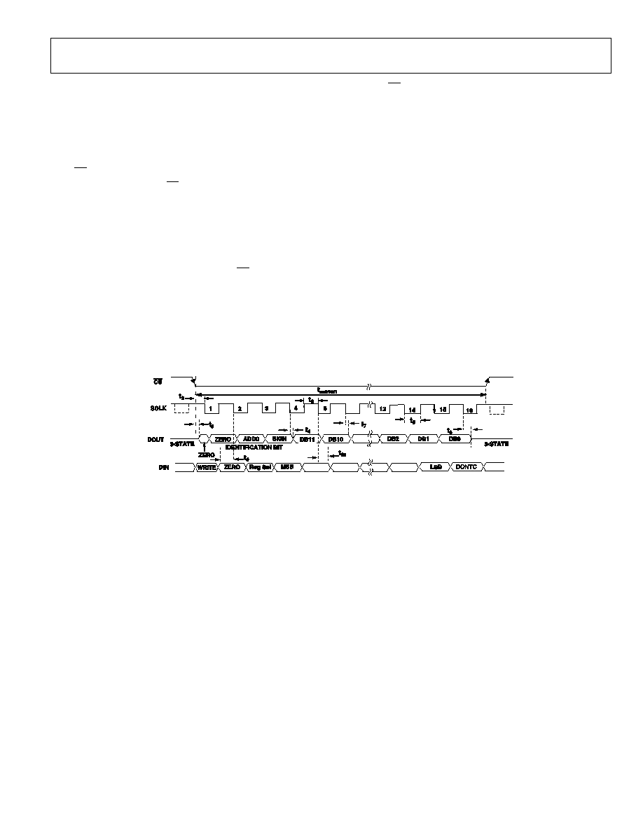
SERIAL INTERFACE
Figure 14
Figure 14. Serial Interface timing Diagram (Control register write)
shows the timing diagram for the serial interface of
the AD7322. The serial clock applied to the SCLK pin provides
the conversion clock and also controls the transfer of
information to and from the AD7322 during a conversion.
The CS signal initiates the data transfer and the conversion
process. The falling edge of CS puts the track-and-hold into
hold mode, take the bus out of three-state and the analog input
signal is sampled at this point. Once the conversion is initiated
it will require 16 SCLK cycles to complete.
The track-and-hold will go back into track on the 15th SCLK
falling edge. On the sixteenth SCLK falling edge, the DOUT line
will return to three-state. If the rising edge of CS occurs before
16 SCLK cycles have elapsed, the conversion will be terminated,
the DOUT line will return to three-state, and depending on
when the CS signal is brought high the addressed register may
or may not be updated. Data is clocked into the AD7322 on the
SCLK falling edge. The three MSB on the DIN line are decoded
to select which register is being addressed. The Control Register
is an eleven bit register, if the control register is addressed by the
three MSB, the data on the DIN line will be loaded into the
Control on the 15
th
SCLK falling edge. If the Range registers is
addressed the data on the DIN line will be loaded into the
addressed register on the 11
th
SCLK falling edge.
Conversion data is clocked out of the AD7322 on each SCLK
falling edge. Data on the DOUT line will consist of two leading
zeros, a channel identifier bit, a Sign bit and the 12-bit
conversion result. The channel identifier bit is used to indicate
which channel the conversion result corresponds to.
Rev. PrE | Page 17 of 18
AD7322
Preliminary Technical Data
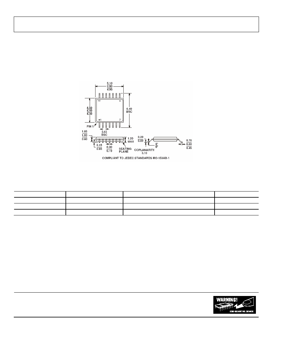
OUTLINE DIMENSIONS
14-Lead Thin Shrink Small Outline (TSSOP)
(RU-14)
Ordering Guide
AD7322 Products
Temperature Package
Package Description
Package Outline
AD7322BRU
40°C to +85°C
TSSOP
RU-14
EVAL-AD7322CB
1
Evaluation
Board
EVAL-CONTROL BRD2
2
Controller
Board
NOTES
1 This can be used as a stand-alone evaluation board or in conjunction with the EVAL-CONTROL Board for evaluation/demonstration purposes.
2 This board is a complete unit allowing a PC to control and communicate with all Analog Devices evaluation boards ending in the CB designators. To order a complete
evaluation kit, the particular ADC evaluation board, e.g., EVAL-AD7322CB, the EVAL-CONTROL BRD2, and a 12V transformer must be ordered. See relevant Evaluation
Board Technical note for more information.
ESD CAUTION
ESD (electrostatic discharge) sensitive device. Electrostatic charges as high as 4000 V readily accumulate on the
human body and test equipment and can discharge without detection. Although this product features
proprietary ESD protection circuitry, permanent damage may occur on devices subjected to high energy
electrostatic discharges. Therefore, proper ESD precautions are recommended to avoid performance
degradation or loss of functionality.
Rev. PrE | Page 18 of 18
PR04863-0-4/04(PrE)
Document Outline