 | –≠–ª–µ–∫—Ç—Ä–æ–Ω–Ω—ã–π –∫–æ–º–ø–æ–Ω–µ–Ω—Ç: AD7468BRM | –°–∫–∞—á–∞—Ç—å:  PDF PDF  ZIP ZIP |
Document Outline
- Specifications
- Package drawings
- Ordering Guide
- Features
- Applications
- Product Description
- Timing characteristics
- Absolute Maximum Ratings
- Functional Block Diagram
- Pin Function Description
- Circuit Description
- CAUTION
- AD7466/ 67/ 68 PINCONFIGURATION
- AD7466/ 67/ 68
- AD7466/ AD7467/ AD7468 TYPICAL PERFORMANCE
- CIRCUIT INFORMATION
- ADC TRANSFER FUNCTION
- CONVERTER OPERATION
- MODE OF OPERATION
- SERIAL INTERFACE
- MICROPROCESSOR INTERFACING
- DIAGRAMS
- Load Circuit for Digital Output Timing Specifications
- AD7466 Dynamic Performance at 100 kSPS
- AD7466 SINAD vs Analog Input Frequency at 100 kSPS
- PSRR vs Supply Ripple Frequency
- AD7466 THD vs Analog Input Frequency at 100 kSPS
- ADC Conversion Phase
- ADC Acquisition Phase
- Equivalent Analog Input Circuit
- REF193 as Power Supply to AD7466/AD7467/ AD7468
- THD vs. Analog Input Frequency for Various Source Impedance
- Normal Mode Operation
- AD7466 Serial Interface Timing Diagram
- AD7467 Serial Interface Timing Diagram
- AD7468 Serial Interface Timing Diagram
- Interfacing to the TMS320C5x
- Interfacing to the ADSP-21xx
- Interfacing to the DSP56xx
- Interfacing to the MC68HC16
AD7466/AD7467/AD7468
a
REV. PrC 07/01
Information furnished by Analog Devices is believed to be accurate and
reliable. However, no responsibility is assumed by Analog Devices for its
use, nor for any infringements of patents or other rights of third parties
which may result from its use. No license is granted by implication or
otherwise under any patent or patent rights of Analog Devices.
One Technology Way, P.O. Box 9106, Norwood, MA 02062-9106, U.S.A.
Tel: 781/329-4700
World Wide Web Site: http://www.analog.com
Fax: 781/326-8703
Analog Devices, Inc., 2001
1.8 V, Micro-Power,
8/10/12-Bit ADCs in 6 Lead SOT-23
Preliminary Technical Data
FUNCTIONAL BLOCK DIAGRAM
FEATURES
Specified for V
DD
of 1.8 V to 3.6 V
Low Power:
0.9 mW max at 60 kSPS with 3.6 V Supplies
0.4 mW max at 100 kSPS with 1.8 V Supplies
Fast Throughput Rate: 100 kSPS
Wide Input Bandwidth:
70dB SNR at 30 kHz Input Frequency
Flexible Power/Serial Clock Speed Management
No Pipeline Delays
High Speed Serial Interface
SPI/QSPI/
µµ
µµ
µ
Wire/DSP Compatible
Standby Mode: 0.5
µ
A max
6-Lead SOT-23 Package and 8 lead
µµ
µµ
µ
SOIC
APPLICATIONS
Battery Powered Systems
Medical Instruments
Ramote Data Acquisition
Isolated Data Acquisition
GENERAL DESCRIPTION
The AD7466/AD7467/AD7468 are 12/10/8-bit, high
speed, low power, successive-approximation ADCs re-
spectively. The parts operate from a single 1.8 V to 3.6 V
power supply and feature throughput rates up to 100
kSPS. The parts contain a low-noise, wide bandwidth
track/hold amplifier which can handle input frequencies in
excess of 100 kHz.
The conversion process and data acquisition are controlled
using
CS and the serial clock, allowing the devices to
interface with microprocessors or DSPs. The input signal
is sampled on the falling edge of
CS and the conversion is
also initiated at this point. There are no pipelined delays
associated with the part.
The AD7466/AD7467/AD7468 use advanced design tech-
niques to achieve very low power dissipation at high
throughput rates.
The reference for the part is taken internally from V
DD.
This allows the widest dynamic input range to the ADC.
Thus the analog input range for the part is 0 to V
DD
. The
conversion rate is determined by the SCLK.
PRODUCT HIGHLIGHTS
1. Specified for Supply voltages of 1.8 V to 3.6 V
2. 8/10/12-Bit ADCs in a SOT-23 package.
3. High Throughput with Low Power Consumption
4 . Flexible Power/Serial Clock Speed Management
The conversion rate is determined by the serial clock
allowing the conversion time to be reduced through the
serial clock speed increase. Automatic power down after
conversion, which allows the average power cunsumption
to be reduced when in powerdown. Power consumption
is 0.5
µ
A max when in powerdown.
5. Reference derived from the power supply.
6. No Pipeline Delay
The part features a standard successive-approximation
ADC with accurate control of the conversions via a
CS
input.
T/H
VIN
AD7466/67/68
VDD
12/10/8-BIT
SUCCESSIVE
APPROXIMATION
ADC
SCLK
CONTROL LOGIC
SDATA
CS
GND
pecifications

≠2≠
REV. PrC
AD7466≠SPECIFICATIONS
1
Parameter
B Version
1, 2
Unit
Test Conditions/Comments
DYNAMIC PERFORMANCE
f
IN
= 30 kHz Sine Wave
Signal-to-Noise + Distortion (SINAD)
2
7 0
dB min
Signal-to-Noise Ratio (SNR)
2
7 1
dB min
Total Harmonic Distortion (THD)
2
≠ 7 8
dB typ
Peak Harmonic or Spurious Noise (SFDR)
2
≠ 8 0
dB typ
Intermodulation Distortion (IMD)
2
fa = 29.1 kHz, fb = 29.9 kHz
Second Order Terms
≠ 7 8
dB typ
Third Order Terms
≠ 7 8
dB typ
Aperture Delay
1 0
ns typ
Aperture Jitter
3 0
ps typ
Full Power Bandwidth
T B D
MHz typ
@ 3 dB
Full Power Bandwidth
T B D
MHz typ
@ 0.1 dB
DC ACCURACY
Resolution
1 2
Bits
Integral Nonlinearity
2
±1.5
LSB max
±0.6
LSB typ
Differential Nonlinearity
2
≠0.9/+1.5
LSB max
Guaranteed No Missed Codes to 12 Bits
±0.75
LSB typ
Offset Error
3
±1.5
LSB max
Gain Error
3
±1.5
LSB max
ANALOG INPUT
Input Voltage Ranges
0 to V
DD
V
DC Leakage Current
±1
µA max
Input Capacitance
3 0
pF typ
LOGIC INPUTS
Input High Voltage, V
INH
0.7(V
DD
)
V min
V
DD
= 1.8 V to 3.6 V
Input Low Voltage, V
INL
0.4
V max
Input Current, I
IN
, SCLK Pin
±1
µA max
Typically 10 nA, V
IN
= 0 V or V
DD
Input Current, I
IN
,
CS
Pin
±1
µA typ
Input Capacitance, C
IN
2,3
1 0
pF max
LOGIC OUTPUTS
Output High Voltage, V
OH
V
DD
≠ 0.2
V min
I
SOURCE
= 200 µA; V
DD
= 1.8 V to 3.6 V
Output Low Voltage, V
OL
0.2
V max
I
SINK
= 200 µA
Floating-State Leakage Current
±10
µA max
Floating-State Output Capacitance
2,3
1 0
pF max
Output Coding
Straight (Natural) Binary
CONVERSION RATE
Conversion Time
6.66
µs max
Sixteen SCLK Cycles
Track/Hold Acquisition Time
T B D
ns max
Full-Scale Step Input
T B D
ns max
Sine Wave Input
Throughput Rate
100
kSPS max See Serial Interface Section
POWER REQUIREMENTS
V
DD
1.8/3.6
V min/max
I
DD
Digital I/Ps = 0 V or V
DD
Normal Mode (Operational)
350
µ
A max
V
DD
= 3 V. SCLK On or Off
200
µ
A max
V
DD
= 1.8 V. SCLK On or Off
Power-Down
0.5
µA max
SCLK Off
8 0
µA max
SCLK On
Power Dissipation
4
Normal Mode (Operational)
T B D
mW max
V
DD
= 3 V. f
SAMPLE
= TBD
mW max
V
DD
= 1.8 V. f
SAMPLE
= TBD
Power-Down
1.5
µW max
V
DD
= 3 V. SCLK Off
0.9
µW max
V
DD
= 1.8 V. SCLK Off
NOTES
1
Temperature ranges as follows: B Versions: ≠40∞C to +85∞C.
2
See Terminology.
3
Sample tested at 25∞C to ensure compliance.
4
See Power Versus Throughput Rate section.
Specifications subject to change without notice.
(V
DD
= 1.8 V to 3.6 V, f
SCLK
= 2.4 MHz, f
SAMPLE
= 100 kSPS unless otherwise noted; T
A
=
T
MIN
to T
MAX
, unless otherwise noted.)
pecifications
≠3≠
REV. PrC
Parameter
B Version
1, 2
Unit
Test Conditions/Comments
DYNAMIC PERFORMANCE
f
IN
= 30 kHz Sine Wave,
Signal-to-Noise + Distortion (SINAD)
2
61
dB min
Total Harmonic Distortion (THD)
2
≠73
dB max
Peak Harmonic or Spurious Noise (SFDR)
2
≠74
dB max
Intermodulation Distortion (IMD)
2
fa = 29.1 kHz, fb = 29.9 kHz
Second Order Terms
≠78
dB typ
Third Order Terms
≠78
dB typ
Aperture Delay
10
ns typ
Aperture Jitter
30
ps typ
Full Power Bandwidth
TBD
MHz typ
@ 3 dB
Full Power Bandwidth
T B D
MHz typ
@ 0.1 dB
DC ACCURACY
Resolution
10
Bits
Integral Nonlinearity
±1
LSB max
Differential Nonlinearity
±0.9
LSB max
Guaranteed No Missed Codes to 10 Bits
Offset Error
±1
LSB max
Gain Error
±1
LSB max
ANALOG INPUT
Input Voltage Ranges
0 to V
DD
V
DC Leakage Current
±1
µA max
Input Capacitance
30
pF typ
LOGIC INPUTS
Input High Voltage, V
INH
0.7(V
DD)
V min
V
DD
= 1.8 to 3.6 V
Input Low Voltage, V
INL
0.4
V max
Input Current, I
IN
, SCLK Pin
±1
µA max
Typically 10 nA, V
IN
= 0 V or V
DD
Input Current, I
IN
,
CS
Pin
±1
µA typ
Input Capacitance, C
IN
2,3
10
pF max
LOGIC OUTPUTS
Output High Voltage, V
OH
V
DD
≠ 0.2
V min
I
SOURCE
= 200 µA;
Output Low Voltage, V
OL
0.2
V max
I
SINK
= 200 µA
Floating-State Leakage Current
±10
µA max
Floating-State Output Capacitance
2,3
10
pF max
Output Coding
Straight (Natural) Binary
CONVERSION RATE
Conversion Time
5
µ
s max
12 SCLK Cycles with SCLK at 20 MHz
Track/Hold Acquisition Time
TBD
ns max
Throughput Rate
100
kSPS max
See Serial Interface Section
POWER REQUIREMENTS
V
D D
1.8/3.6
V min/max
I
D D
Digital I/Ps = 0 V or V
DD
Normal Mode (Operational)
350
µ
A max
V
DD
= 3 V . SCLK On or Off
200
µ
A max
V
DD
= 1.8 V . SCLK On or Off
Power-Down Mode
0.5
µA max
SCLK Off
80
µA max
SCLK On
Power Dissipation
4
Normal Mode (Operational)
TBD
mW max
V
DD
= 3 V. f
SAMPLE
= 100 kSPS
TBD
mW max
V
DD
= 1.8 V. f
SAMPLE
= TBD
Power-Down
1.5
µW max
V
DD
= 3 V. SCLK Off
0.9
µW max
V
DD
= 1.8 V. SCLK Off
NOTES
1
Temperature ranges as follows: B Versions: ≠40∞C to +85∞C.
2
See Terminology.
3
Sample tested at 25∞C to ensure compliance.
4
See Power Versus Throughput Rate section.
Specifications subject to change without notice.
AD7467≠SPECIFICATIONS
1
(V
DD
= 1.8 V to 3.6 V, f
SCLK
= 2.4 MHz, f
SAMPLE
= 100 kSPS unless otherwise noted; T
A
=
T
MIN
to T
MAX
, unless otherwise noted.)
pecifications
≠4≠
REV. PrC
Parameter
B Version
1, 2
Unit
Test Conditions/Comments
DYNAMIC PERFORMANCE
f
IN
=30 kHz Sine Wave, f
SAMPLE
=100kSPS
Signal-to-Noise + Distortion (SINAD)
2
49
dB min
Total Harmonic Distortion (THD)
2
≠65
dB max
Peak Harmonic or Spurious Noise (SFDR)
2
≠65
dB max
Intermodulation Distortion (IMD)
2
fa = 29.1 kHz, fb = 29.9 kHz
Second Order Terms
≠68
dB typ
Third Order Terms
≠68
dB typ
Aperture Delay
10
ns typ
Aperture Jitter
30
ps typ
Full Power Bandwidth
TBD
MHz typ
@ 3 dB
Full Power Bandwidth
T B D
MHz typ
@ 0.1 dB
DC ACCURACY
2
Resolution
8
Bits
Integral Nonlinearity
±0.5
LSB max
Differential Nonlinearity
±0.5
LSB max
Guaranteed No Missed Codes to 8 Bits
Offset Error
±0.5
LSB max
Gain Error
±0.5
LSB max
Total Unadjusted Error (TUE)
±0.5
LSB max
ANALOG INPUT
Input Voltage Ranges
0 to V
DD
V
DC Leakage Current
±1
µA max
Input Capacitance
30
pF typ
LOGIC INPUTS
Input High Voltage, V
INH
0.7(V
DD)
V min
V
DD
= 1.8 to 3.6 V
Input Low Voltage, V
INL
0.4
V max
Input Current, I
IN
, SCLK Pin
±1
µA max
Typically 10 nA, V
IN
= 0 V or V
DD
Input Current, I
IN
,
CS
Pin
±1
µA typ
Input Capacitance, C
IN
2,3
10
pF max
LOGIC OUTPUTS
Output High Voltage, V
OH
V
DD
≠ 0.2
V min
I
SOURCE
= 200 µA; V
DD
= 1.8 V to 3.6 V
Output Low Voltage, V
OL
0.2
V max
I
SINK
= 200 µA
Floating-State Leakage Current
±10
µA max
Floating-State Output Capacitance
3, 4
10
pF max
Output Coding
Straight (Natural) Binary
CONVERSION RATE
Conversion Time
4.166
µ
s max
10 SCLK Cycles with SCLK at 2.4 MHz
Track/Hold Acquisition Time
TBD
ns max
Throughput Rate
100
kSPS max
See Serial Interface Section
POWER REQUIREMENTS
V
D D
1.8/3.6
V min/max
I
D D
Digital I/Ps = 0 V or V
DD
Normal Mode (Static)
350
µ
A max
V
DD
= 3V. SCLK On or Off
200
µ
A max
V
DD
= 1.8 V . SCLK On or Off
Power-Down Mode
0.5
µA max
SCLK Off
80
µA max
SCLK On
Power Dissipation
5
Normal Mode (Operational)
TBD
mW max
V
DD
= 3 V. f
SAMPLE
= TBD
TBD
mW max
V
DD
= 1.8 V. f
SAMPLE
= TBD
Power-Down
1.5
µW max
V
DD
= 3 V. SCLK Off
0.9
µW max
V
DD
= 1.8 V. SCLK Off
NOTES
1
Temperature ranges as follows: B Versions: ≠40∞C to +85∞C.
2
See Terminology.
3
Sample tested at 25∞C to ensure compliance.
4
See Power Versus Throughput Rate section.
Specifications subject to change without notice.
AD7468≠SPECIFICATIONS
1
(V
DD
= 1.8 V to 3.6 V, f
SCLK
= 2.4 MHz, f
SAMPLE
= 100 kSPS unless otherwise noted; T
A
=
T
MIN
to T
MAX
, unless otherwise noted.)
pecifications
AD7466/AD7467/AD7468
≠5≠
REV. PrC
Parameter
AD7466
Units
Description
f
SCLK
2
10
kHz min
T B D
MHz max
t
CONVERT
16* t
SCLK
t
quiet
T B D
ns min
Minimum Quiet Time required between Bus Relinquish
and start of next conversion
t
1
T B D
ns min
Minimum
CS Pulse Width
t
2
10
ns min
CS to SCLK Setup Time
t
3
3
T B D
ns max
Delay from
CS Until SDATA 3-State Disabled
t
4
3
T B D
ns max
Data Access Time After SCLK Falling Edge
t
5
0.4t
SCLK
ns min
SCLK Low Pulse Width
t
6
0.4t
SCLK
ns min
SCLK High Pulse Width
t
7
T B D
ns min
SCLK to Data Valid Hold Time
t
8
4
T B D
ns max
SCLK falling Edge to SDATA High Impedance
t
power-up
5
T B D
µ
s typ
Power up time from Full Power-down.
TIMING SPECIFICATIONS
1
NOTES
1
Sample tested at +25∞C to ensure compliance. All input signals are specified with tr = tf = 5 ns (10% to 90% of V
DD
) and timed from a voltage level of 1.6 Volts.
2
Mark/Space ratio for the SCLK input is 40/60 to 60/40.
3
Measured with the load circuit of Figure 1 and defined as the time required for the output to cross 0.8 V or 2.0 V.
4
t
8
is derived form the measured time taken by the data outputs to change 0.5 V when loaded with the circuit of Figure 1. The measured number is then extrapolated back to
remove the effects of charging or discharging the 50 pF capacitor. This means that the time, t
8
, quoted in the timing characteristics is the true bus relinquish time of the
part and is independent of the bus loading.
5
See Power-up Time section.
Specifications subject to change without notice.
(V
DD
= +1.8 V to +3.6 V; T
A
= T
MIN
to T
MAX
, unless otherwise noted.)
CAUTION
ESD (electrostatic discharge) sensitive device. Electrostatic charges as high as 4000 V readily
accumulate on the human body and test equipment and can discharge without detection.
Although the AD7466/AD7467/AD7468 feature proprietary ESD protection circuitry, per-
manent damage may occur on devices subjected to high energy electrostatic discharges. There-
fore, proper ESD precautions are recommended to avoid performance degradation or loss of
functionality.
ABSOLUTE MAXIMUM RATINGS
1
(T
A
= +25∞C unless otherwise noted)
V
DD
to GND
≠0.3 V to TBD V
Analog Input Voltage to GND
≠0.3 V to V
DD
+ 0.3 V
Digital Input Voltage to GND
≠0.3 V to TBDV
Digital Output Voltage to GND
≠0.3 V to V
DD
+ 0.3 V
Input Current to Any Pin Except Supplies
2
±10 mA
Operating Temperature Range
Commercial (A, B Version)
≠40∞C to +85∞C
Storage Temperature Range
≠65∞C to +150∞C
Junction Temperature
+150∞C
SOT-23 Package, Power Dissipation
450 mW
JA
Thermal Impedance 229.6∞C/W (SOT23)
205.9∞C/W (µSOIC)
JC
Thermal Impedance 91.99∞C/W (SOT23)
43.74∞C/W (µSOIC)
Lead Temperature, Soldering
Vapor Phase (60 secs)
+215∞C
Infared (15 secs)
+220∞C
E S D
T B D
NOTES
1
Stresses above those listed under "Absolute Maximum Ratings" may cause permanent
damage to the device. This is a stress rating only and functional operation of the device
at these or any other conditions above those listed in the operational sections of this
specification is not implied. Exposure to absolute maximum rating conditions for
extended periods may affect device reliability.
2
Transient currents of up to 100 mA will not cause SCR latch up.
Figure 1. Load Circuit for Digital Output Timing
Specifications
+1.6V
IO L
200µ A
200µ A
IO H
T O
O UT P UT
P IN
C L
50p F
pecifications
AD7466/AD7467/AD7468
≠6≠
REV. PrC
PIN FUNCTION DESCRIPTION
Pin
Pin
No.
Mnemonic
Function
6
C S
Chip Select. Active low logic input. This input provides the dual function of initiating con-
versions on the AD7466/AD7467/AD7468 and also frames the serial data transfer.
1
V
DD
Power Supply Input. The V
DD
range for the AD7466/67/68 is from +1.8 V to +3.6 V.
2
G N D
Analog Ground. Ground reference point for all circuitry on the AD7466/AD7467/AD7468.
All analog input signals should be referred to this GND voltage.
3
V
IN
Analog Input. Single-ended analog input channel. The input range is 0 to V
DD
.
5
SDATA
Data Out. Logic Output. The conversion result from the AD7466/AD7467/AD7468 is pro-
vided on this output as a serial data stream. The bits are clocked out on the falling edge of
the SCLK input. The data stream from the AD7466 consists of four leading zeros followed
by the 12 bits of conversion data which is provided MSB first. The data stream for the
AD7467 consists of four leading zeros followed by 10 bits of data. The datastream for the
AD7468 consists of four leading zeros followed by 8 bits of data.
4
SCLK
Serial Clock. Logic input. SCLK provides the serial clock for accessing data from the part.
This clock input is also used as the clock source for the AD7466/AD7467/AD7468 conver-
sion process.
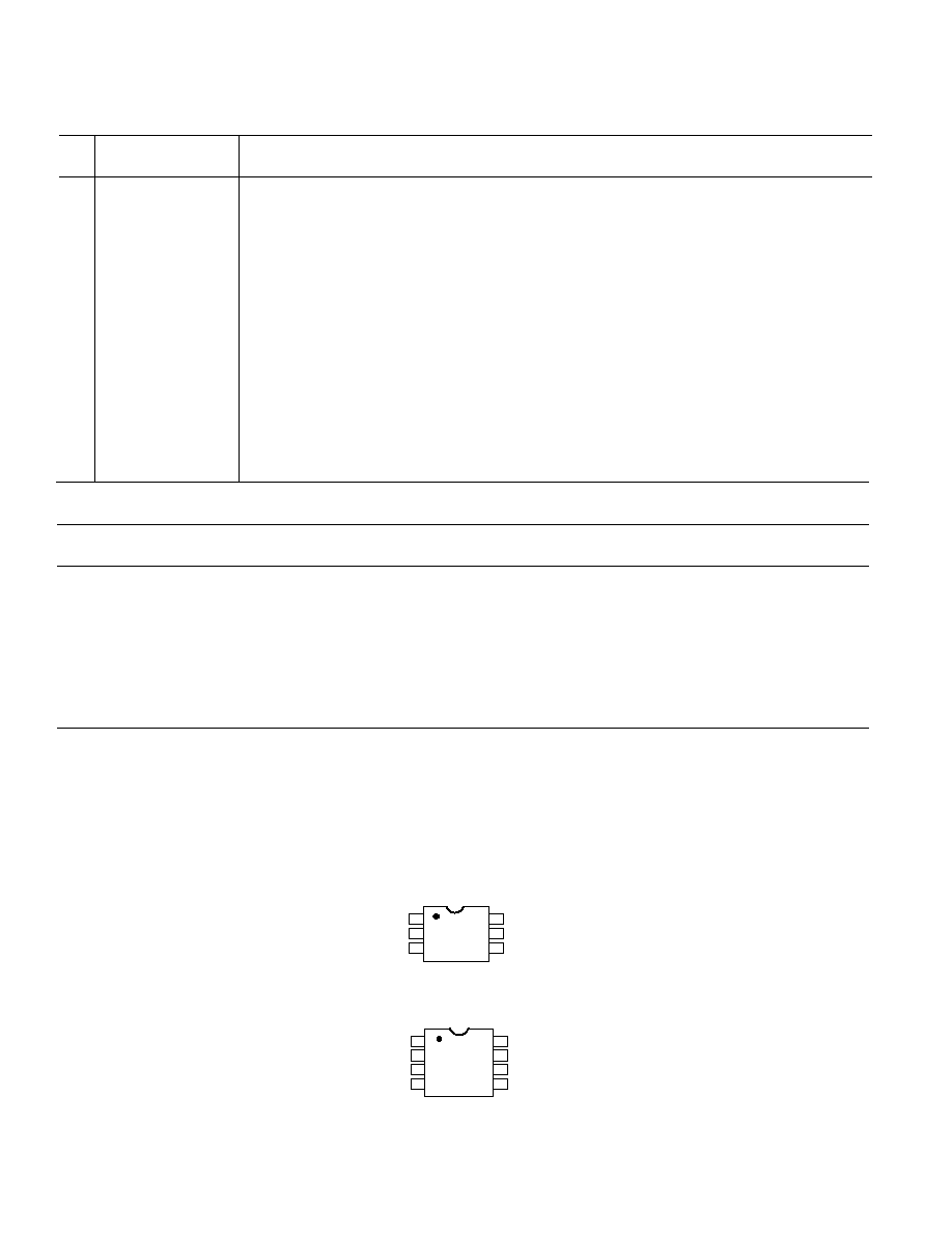
AD7466/67/68 PINCONFIGURATION
AD7466/7/8
TOP VIEW
1
2
3
4
5
6
CS
SDATA
SCLK
VDD
GND
VIN
(Not to Scale)
ORDERING GUIDE
Temperature
Linearity
Package
Branding
Model
Range
Error (LSB)
1
Option
2
Information
AD7466BRT
≠40∞C to +85∞C
±1 max
RT-6
C L B
AD7467BRT
≠40∞C to +85∞C
±1 max
RT-6
C M B
AD7468BRT
≠40∞C to +85∞C
±0.5 max
RT-6
C N B
AD7466BRM
≠40∞C to +85∞C
±1 max
RM-8
C Q B
AD7467BRM
≠40∞C to +85∞C
±1 max
RM-8
CRB
AD7468BRM
≠40∞C to +85∞C
±0.5 max
RM-8
C S B
EVAL-AD7466CB
3
EVAL-AD7467CB
3
EVAL-CONTROL BRD2
4
NOTES
1
Linearity Error here refers to integral linearity error.
2
RT = SOT-23, RM =
µ
SOIC.
3
This can be used as a stand-alone evaluation board or in conjunction with the EVAL-CONTROL BOARD for evaluation/demonstration purposes.
4
This board is a complete unit allowing a PC to control and communicate with all Analog Devices evaluation boards ending in the CB designators.
AD7466/7/8
TOP VIEW
1
2
3
4
5
6
7
8
NC
CS
SDATA
SCLK
VDD
GND
VIN
(Not to Scale)
NC
AD7466/67/68 SOT-23
AD7466/67/68
µ
µ
µ
µ
µ
SOIC
pecifications

AD7466/AD7467/AD7468
≠7≠
REV. PrC
TERMINOLOGY
Integral Nonlinearity
This is the maximum deviation from a straight line pass-
ing through the endpoints of the ADC transfer function.
For the AD7466/67/68 the endpoints of the transfer
function are zero scale, a point 1 LSB below the first
code transition, and full scale, a point 1 LSB above the
last code transition.
Differential Nonlinearity
This is the difference between the measured and the ideal 1
LSB change between any two adjacent codes in the ADC.
Offset Error
This is the deviation of the first code transition (00 . . .
000) to (00 . . . 001) from the ideal, i.e AGND + 1
LSB.
Gain Error
This is the deviation of the last code transition (111 . . .
110) to (111 . . . 111) from the ideal (i.e., V
REF
≠ 1LSB)
after the offset error has been adjusted out.
Track/Hold Acquisition Time
The track/hold amplifier returns into track mode at the
end of conversion. Track/Hold acquisition time is the
time required for the output of the track/hold amplifier
to reach its final value, within ±0.5 LSB, after the end
of conversion. See serial interface timing section for
more details.
Signal to (Noise + Distortion) Ratio
This is the measured ratio of signal to (noise + distor-
tion) at the output of the A/D converter. The signal is
the rms amplitude of the fundamental. Noise is the sum
of all nonfundamental signals up to half the sampling
frequency (f
S
/2), excluding dc. The ratio is dependent on
the number of quantization levels in the digitization
process; the more levels, the smaller the quantization
noise. The theoretical signal to (noise + distortion) ratio
for an ideal N-bit converter with a sine wave input is
given by:
Signal to (Noise + Distortion) = (6.02 N + 1.76) dB
Thus for a 12-bit converter, this is 74 dB and for a 10-
bit converter this is 62dB.
Total Harmonic Distortion
Total harmonic distortion (THD) is the ratio of the rms
sum of harmonics to the fundamental. For the AD7466/
AD7467/AD7468, it is defined as:
where V
1
is the rms amplitude of the fundamental and V
2
,
V
3
, V
4
, V
5
and V
6
are the rms amplitudes of the second
through the sixth harmonics.
Peak Harmonic or Spurious Noise
Peak harmonic or spurious noise is defined as the ratio of
the rms value of the next largest component in the ADC
output spectrum (up to f
S
/2 and excluding dc) to the rms
value of the fundamental. Normally, the value of this
specification is determined by the largest harmonic in the
spectrum, but for ADCs where the harmonics are buried
in the noise floor, it will be a noise peak.
Intermodulation Distortion
With inputs consisting of sine waves at two frequencies, fa
and fb, any active device with nonlinearities will create
distortion products at sum and difference frequencies of
mfa ± nfb where m, n = 0, 1, 2, 3, etc. Intermodulation
distortion terms are those for which neither m nor n are
equal to zero. For example, the second order terms in-
clude (fa + fb) and (fa ≠ fb), while the third order terms
include (2fa + fb), (2fa ≠ fb), (fa + 2fb) and (fa ≠ 2fb).
The AD7466/AD7467/AD7468 are tested using the CCIF
standard where two input frequencies are used. In this
case, the second order terms are usually distanced in fre-
quency from the original sine waves while the third order
terms are usually at a frequency close to the input frequen-
cies. As a result, the second and third order terms are
specified separately. The calculation of the
intermodulation distortion is as per the THD specification
where it is the ratio of the rms sum of the individual dis-
tortion products to the rms amplitude of the sum of the
fundamentals expressed in dBs.
THD (dB )
=
20 log
V
2
2
+
V
3
2
+
V
4
2
+
V
5
2
+
V
6
2
V
1
pecifications
AD7466/AD7467/AD7468
≠8≠
REV. PrC
AD7466/AD7467/AD7468 TYPICAL PERFORMANCE
C U R V E S
Figure 2 shows a typical FFT plot for the AD7466 at 100
kHz sample rate and 30 kHz input frequency.
Figure 2. AD7466 Dynamic Performance at 100 kSPS
TITLE
0
0
0
0
0
0
T
IT
L
E
0
0
0
0
TITLE
0
0
0
0
0
0
T
IT
L
E
0
0
0
0
TITLE
0
0
0
0
0
0
T
IT
L
E
0
0
0
0
Figure 3. AD7466 SINAD vs Analog Input Frequency at 100
kSPS
Figure 5. AD7466 THD vs Analog Input Frequency at 100
kSPS
TITLE
0
0
0
0
0
0
T
IT
L
E
0
0
0
0
Figure 4. PSRR vs Supply Ripple Frequency
pecifications
AD7466/AD7467/AD7468
≠9≠
REV. PrC
CIRCUIT INFORMATION
The AD7466/AD7467/AD7468 are fast, micro-power, 12/
10/8-bit, A/D converters respectively. The parts can be
operated from a +1.8 V to +3.6 V supply. When operated
from any supply voltage within this range, the AD7466/
AD7467/AD7468 is capable of throughput rates of 100
kSPS when provided with a 2 MHz clock.
The AD7466/AD7467/AD7468 provides the user with an
on-chip track/hold, A/D converter, and a serial interface
housed in a tiny 6-pin SOT-23 package, which offers the
user considerable space saving advantages over alternative
solutions. The serial clock input accesses data from the
part but also provides the clock source for the successive-
approximation A/D converter. The analog input range is 0
to V
DD
. An external reference is not required for the ADC
and neither is there a reference on-chip. The reference for
the AD7466/AD7467/AD7468 is derived from the power
supply and thus gives the widest dynamic input range.
The AD7466/AD7467/AD7468 also features an automatic
power-down mode option to allow power saving between
conversions. The power-down feature is implemented
across the standard serial interface as described in the
"Modes of Operation" section.
ADC TRANSFER FUNCTION
The output coding of the AD7466/AD7467/AD7468 is
straight binary. The designed code transitions occur at
successive integer LSB values (i.e., 1LSB, 2LSBs, etc.).
The LSB size is = V
DD
/4096 for the AD7466,the LSB size
is = V
DD
/1024 for the AD7467, and the LSB size is =
V
DD
/256 for the AD7468 . The ideal transfer characteristic
for the AD7466/AD7467/AD7468 is shown in figure 10
below.
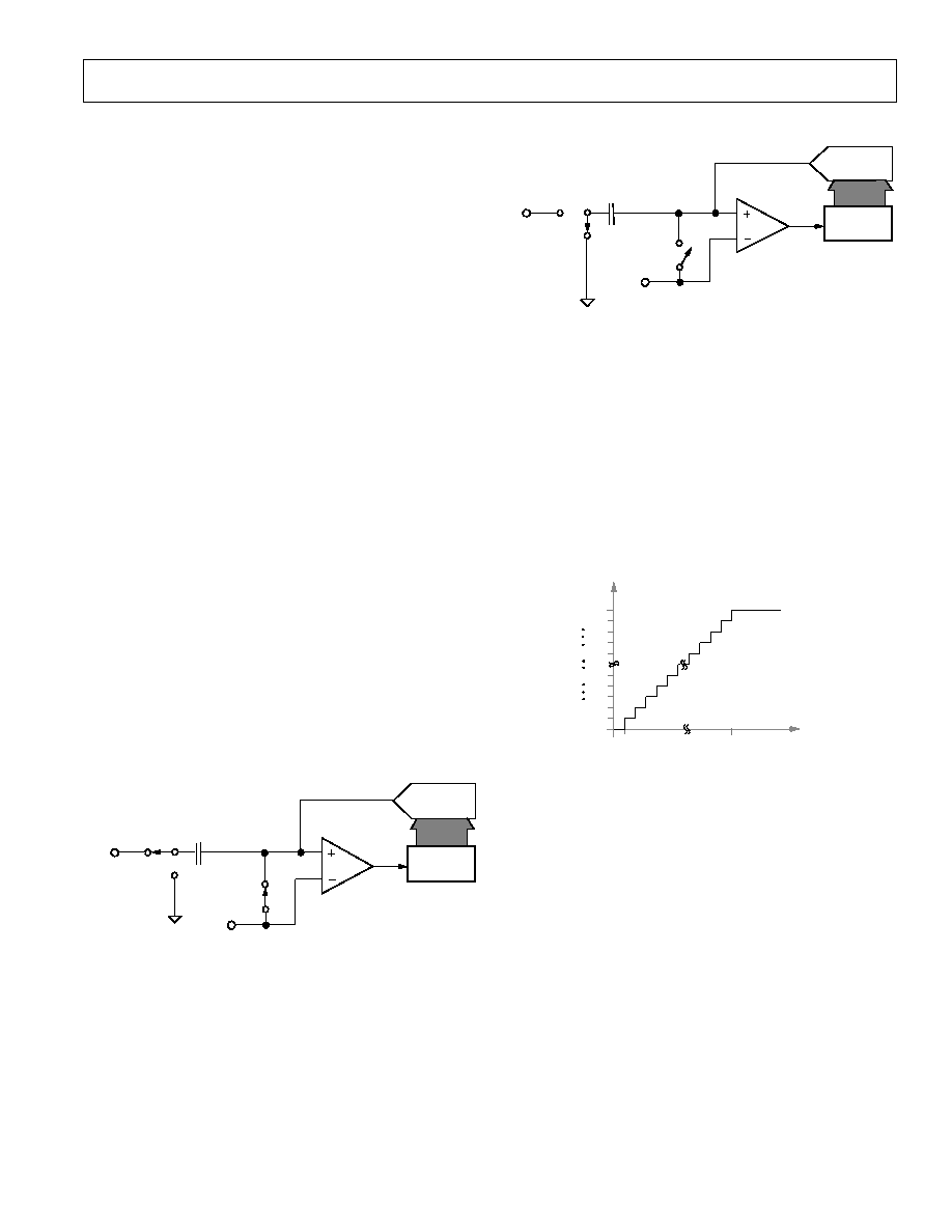
CONVERTER OPERATION
The AD7466/AD7467/AD7468 is a successive approxi-
mation analog-to-digital converter based around a charge
redistribution DAC. Figures 8 and 9 show simplified
schematics of the ADC. Figure 8 shows the ADC during
its acquisition phase. SW2 is closed and SW1 is in posi-
tion A, the comparator is held in a balanced condition and
the sampling capacitor acquires the signal on V
IN
.
When the ADC starts a conversion, see figure 9, SW2 will
open and SW1 will move to position B causing the com-
parator to become unbalanced. The Control Logic and
the Charge Redistribution DAC are used to add and sub-
tract fixed amounts of charge from the sampling capacitor
to bring the comparator back into a balanced condition.
When the comparator is rebalanced the conversion is com-
plete. The Control Logic generates the ADC output code.
Figure 10 shows the ADC transfer function.
Figure 8. ADC Acquisition Phase
Figure 9. ADC Conversion Phase
Figure 10. AD7466/67/68 Transfer Characteristic
C H A R G E
R E D I S T R I B U T I O N
D A C
V I N
V D D / 2
S A M P L I N G
C A P A C I T O R
C O M P A R A T O R
C O N T R O L
L O G I C
A C Q U I S I T I O N
P H A S E
S W 1
A
B
S W 2
A G N D
CHARGE
REDISTRIBUTION
DA C
VIN
VDD / 2
SAMPLING
CAPACITOR
COMPAR ATOR
CONTROL
LO GIC
CONVERSION
PHASE
SW1
A
B
SW2
AGND
000...000
0V
A
D
C
C
O
D
E
ANAL OG INPUT
111...111
000...001
000...010
111...110
111...000
011...111
1LSB
+VDD-1LSB
1LSB = VDD/4096 (AD7466)
1LSB = VDD/1024 (AD7467)
1LSB = VDD/256 (AD7468)
pecifications
AD7466/AD7467/AD7468
≠10≠
REV. PrC
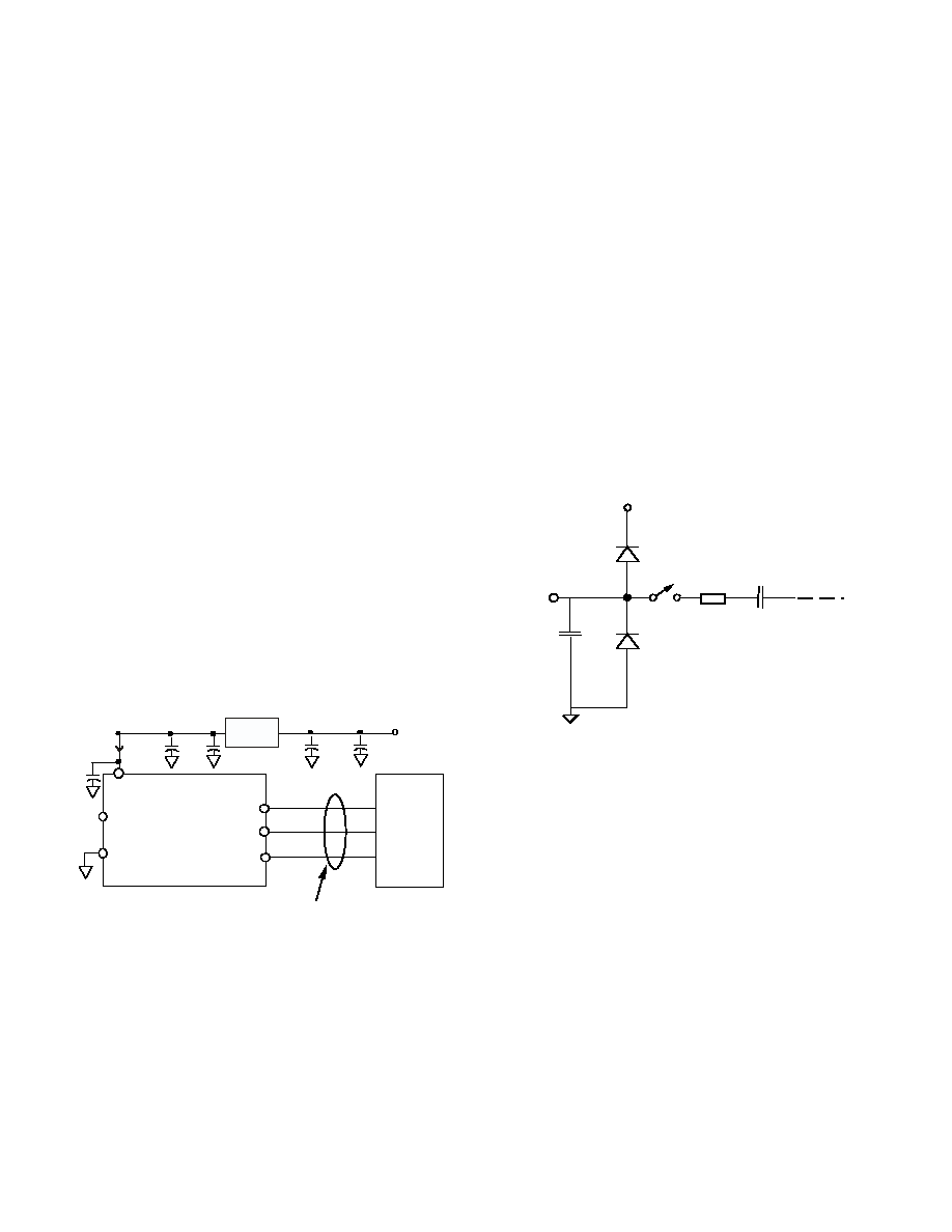
Figure 11. REF193 as Power Supply to AD7466/AD7467/
AD7468
Analog Input
Figure 12 shows an equivalent circuit of the analog input
sturcture of the AD7466/AD7467/7468. The two diodes
D1 and D2 provide ESD protection for the analog inputs.
Care must be taken to ensure that the analog input signal
never exceeds the supply rails by more than 200mV. This
will cause these diodes to become forward biased and start
conducting current into the substrate. The capacitor C1 in
figure 12 is typically about 4pF and can primarily be at-
tributed to pin capacitance. The resistor R1 is a lumped
component made up of the on resistance of a switch. This
resistor is typically about 100
.
The capacitor C2 is the
ADC sampling capacitor and has a capacitance of 16pF
typically. For ac applications, removing high frequency
components from the analog input signal is recommended
by use of a band-pass filter on the relevant analog input
pin. In applications where harmonic distortion and signal
to noise ratio are critical the analog input should be driven
VIN
D1
VDD
D2
R1
C2
16PF
C1
4pF
CONVERSION PHASE - SWITCH OPEN
TRACK PHASE - SWITCH CLOSED
from a low impedance source. Large source impedances
will significantly affect the ac performance of the ADC.
This may necessitate the use of an input buffer amplifier.
The choice of the op amp will be a function of the par-
ticular application.
When no amplifier is used to drive the analog input the
source impedance should be limited to low values. The
maximum source impedance will depend on the amount of
total harmonic distortion (THD) that can be tolerated.
The THD will increase as the source impedance increases
and performance will degrade. Figure 13 shows a graph of
the Total Harmonic Distortion vs. analog input signal
frequency for different source impedances when using a
supply voltage of 2.7V and sampling at a rate of 100
kSPS.
Figure 12. Equivalent Analog Input Circuit
V
DD
VIN
GND
+5V
SUPPLY
0.1µF
10µF
REF193
0.1µF
1µF
TANT
+3V
AD7466/67/68
0V toVDD
INPUT
SDATA
µC/µP
SCLK
SERIAL
INTERFACE
CS
1mA
680nF
The AD7468 conversion result consists of four leading
zeros followed by the MSB of the 8-bit result.
Alternatively, because the supply current required by the
AD7466/AD7467/AD7468 is so low, a presision reference
can be used as the supply source to the AD7466/AD7467/
AD7468. A REF19x voltage reference (REF193 for 3V,
REF192 for 2.5 V ) can be used to supply the required
voltage to the ADC - see figure 11. This configuration is
especially useful if your power supply is quite noisy or if
the system supply voltages are at some value other than 3V
(e.g. 2.5V). The REF19x will output a steady voltage to
the AD7466/AD7467/AD7468. In applications where
power consumption is important, the automatic power
down mode of the ADC and the sleep mode of the
REF19x reference should be used to improve power per-
formance. See Modes of Operation section of the
datasheet.
TYPICAL CONNECTION DIAGRAM
Figure 11 shows a typical connection diagram for the
AD7466/AD7467/AD7468. V
REF
is taken internally from
V
DD
and as such V
DD
should be well decoupled. This pro-
vides an analog input range of 0V to V
DD
. For the
AD7466 the conversion result is output in a 16-bit word
with four leading zeroes followed by the MSB of the 12-
bit result. The AD7467 conversion result consists of four
leading zeros followed by the MSB of the 10-bit result.
pecifications
AD7466/AD7467/AD7468
≠11≠
REV. PrC
Digital Inputs
The digital inputs applied to the AD7466/AD7467/
AD7468 are not limited by the maximum ratings which
limit the analog inputs. One advantage of SCLK and
CS
not being restricted by the V
DD
+ 0.3V limit is the fact that
power supply sequencing issues are avoided. If
CS or
SCLK are applied before V
DD
then there is no risk of
latch-up as there would be on the analog inputs if a signal
greater than 0.3V was applied prior to V
DD
.
MODE OF OPERATION
The AD7466/AD7467/AD7468 automatically enters
powerdown at the end of each conversion. This mode of
operation is designed to provide flexible power manage-
ment options and to optimize the power dissipation/
throughput rate ratio for differing application require-
ments. Figure 14 shows the general diagram of the
operaion of the AD7466/AD7467/AD7468. On the falling
CS edge the part begins to power up and the Track and
Hold, which was in Hold while the part was in power
down, will go into track mode. When operating the part
with a 2.4 MHz clock it will take 2 clock cycles to fully
power up the part and acquire the input signal. On the
third SCLK falling edge after the
CS falling edge the
Track and Hold will return to hold mode. For the
AD7466 sixteen serial clock cycles are required to com-
plete the conversion and access the complete conversion
result.On the 16th SCLK falling edge the part will auto-
matically enter power down . The AD7467 will automati-
cally enter powerdown on the fourteenth SCLK falling
edge. The AD7468 will automatically enter powerdown
on the twelveth SCLK falling edge. When supplies are
first applied to the AD7466/AD7467/AD7468 a dummy
conversion should be performed to ensure that the part is
in powerdown mode.
The conversion is iniated on the falling edge of
CS as
described in the Serial Interface section. For the AD7466
if
CS is brought high any time before the 16th SCLK
falling edge the part will enter power down and the con-
version that was initiated by the falling edge of
CS will be
terminated and SDATA will go back into tri-state. This
also applies for the AD7467/AD7468, if
CS is brought
high before the conversion is complete (the 14th SCLK
falling edge for the AD7467, and the 12th SCLK falling
edge for the AD7468) the part will enter powerdown and
the conversion will be terminated.
Once a data transfer is complete (SDATA has returned to
tri-state), another conversion can be initiated after the
quiet time, t
quiet
, has elapsed by bringing
CS low again.
VALIDDATA
16
1
THE PART BEGINS
TO POWER UP
3
AD7466 ENTERS
POWERDOWN
2
AD7467 ENTERS
POWERDOWN
AD7468 ENTERS
POWERDOWN
14
12
Figure 14. Normal Mode Operation
Figure 13. THD vs. Analog Input Frequency for Various
Source Impedance
TITLE
0
0
0
0
0
0
T
IT
L
E
0
0
0
0
pecifications
AD7466/AD7467/AD7468
≠12≠
REV. PrC
SERIAL INTERFACE
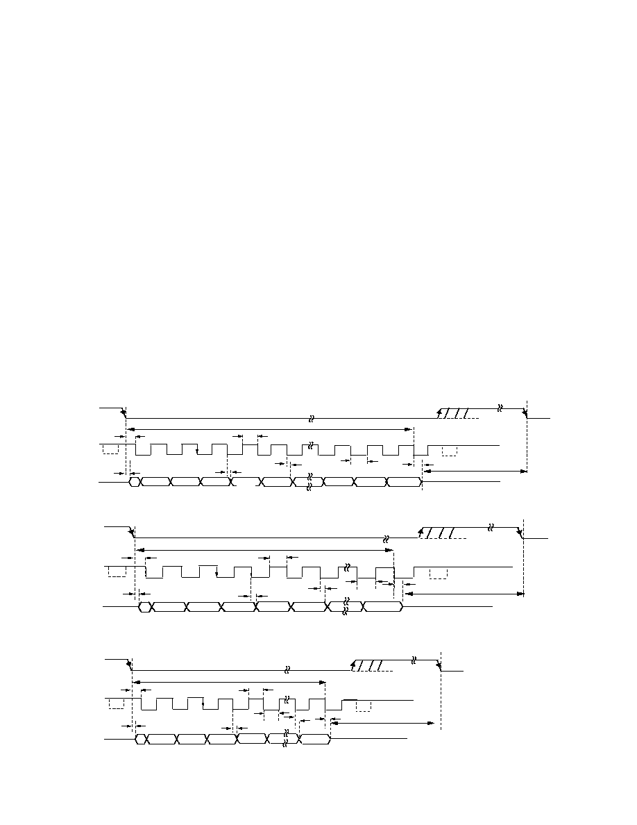
Figure 15, 16, 17 show the detailed timing diagram for
serial interfacing to the AD7466/AD7467/AD7468.The
serial clock provides the conversion clock and also con-
trols the transfer of information from the ADC during a
conversion.
On the
CS falling edge the part begins to power up. The
falling edge of
CS puts the track and hold into track mode
and takes the bus out of tristate. The conversion is also
initiated at this point and will require 16 SCLK cycles to
complete. On the third SCLK falling edge the part should
be fully powered up, as shown in figure 15 at point B. On
the third SCLK falling edge after the CS falling edge the
track and hold will return to hold. On the 16th SCLK
falling edge the SDATA line will go back into tristate and
the AD7466 will enter power down. If the rising edge of
CS occurs before 16 SCLKs have elapsed then the conver-
sion will be terminated and the SDATA line will go back
into tri-state and the part will enter power down, otherwise
SDATA returns to tri-state on the 16th SCLK falling
edge as shown in Figure 15. Sixteen serial clock cycles
are required to perform the conversion process and to
access data from the AD7466.
For the AD7467, the fourteenth SCLK falling edge will
cause the SDATA line to go back into tri-state and the
part will enter powerdown. If the rising edge of CS occurs
before 14 SCLKs have elapsed then the conversion will be
terminated and the SDATA line will go back into tri-state
and the AD7467 will enter powerdown, otherwise SDATA
returns to tri-state on the 14th SCLK falling edge as
ahown in figure 16. Fourteen serial clock cycles are re-
quired to perform the conversion process and to access
data from the AD7467.
For the AD7468, the 12th SCLK falling edge will cause
the SDATA line to go back into tri-state and the part will
enter powerdown. If the rising edge of CS occurs before
12 SCLKs have elapsed then the conversion will be termi-
nated and the SDATA line will go back into tri-state and
the AD7468 will enter powerdown, otherwise SDATA
returns to tri-state on the 12th SCLK falling edge as
ahown in figure 17. Twelve serial clock cycles are re-
quired to perform the conversion process and to access
data from the AD7468.
CS going low provides the first leading zero to be read in
by the microcontroller or DSP. The remaining data is
then clocked out by subsequent SCLK falling edges be-
ginning with the 2nd leading zero, thus the first falling
clock edge on the serial clock has the first leading zero
provided and also clocks out the second leading zero. For
the Ad7466 the final bit in the data transfer is valid on the
sixteenth falling edge, having being clocked out on the
previous (15th) falling edge.
Figure 15. AD7466 Serial Interface Timing Diagram
Figure 16. AD7467 Serial Interface Timing Diagram
CS
SCLK
1
5
13
SDATA
4 LEAD IN G ZERO'S
3-STATE
t
4
2
3
4
t
3
t
qu iet
t
c on v ert
t
2
3-STATE
DB9
DB8
DB0
t
6
t
7
t
8
14
ZERO
ZERO
ZERO
Z
B
t
5
CS
t
quiet
3-STATE
t
5
t
8
B
DB0
t
7
SCLK
1
SDATA
4 LEADING ZERO'S
ZERO
ZERO
ZERO
Z
3-STATE
t
4
2
3
4
t
3
t
convert
t
2
DB7
t
6
8 BITS OF DATA
12
11
Figure 17. AD7468 Serial Interface Timing Diagram
CS
SCLK
1
5
13
15
SDATA
4 LEADING ZERO'S
3-STATE
t
4
2
3
4
16
t
5
t
3
t
quie
t
t
convert
t
2
3-STATE
DB11
DB10
DB2
DB0
t
6
t
7
t
8
14
ZERO
ZERO
ZERO
Z
B
DB1
pecifications
AD7466/AD7467/AD7468
≠13≠
REV. PrC
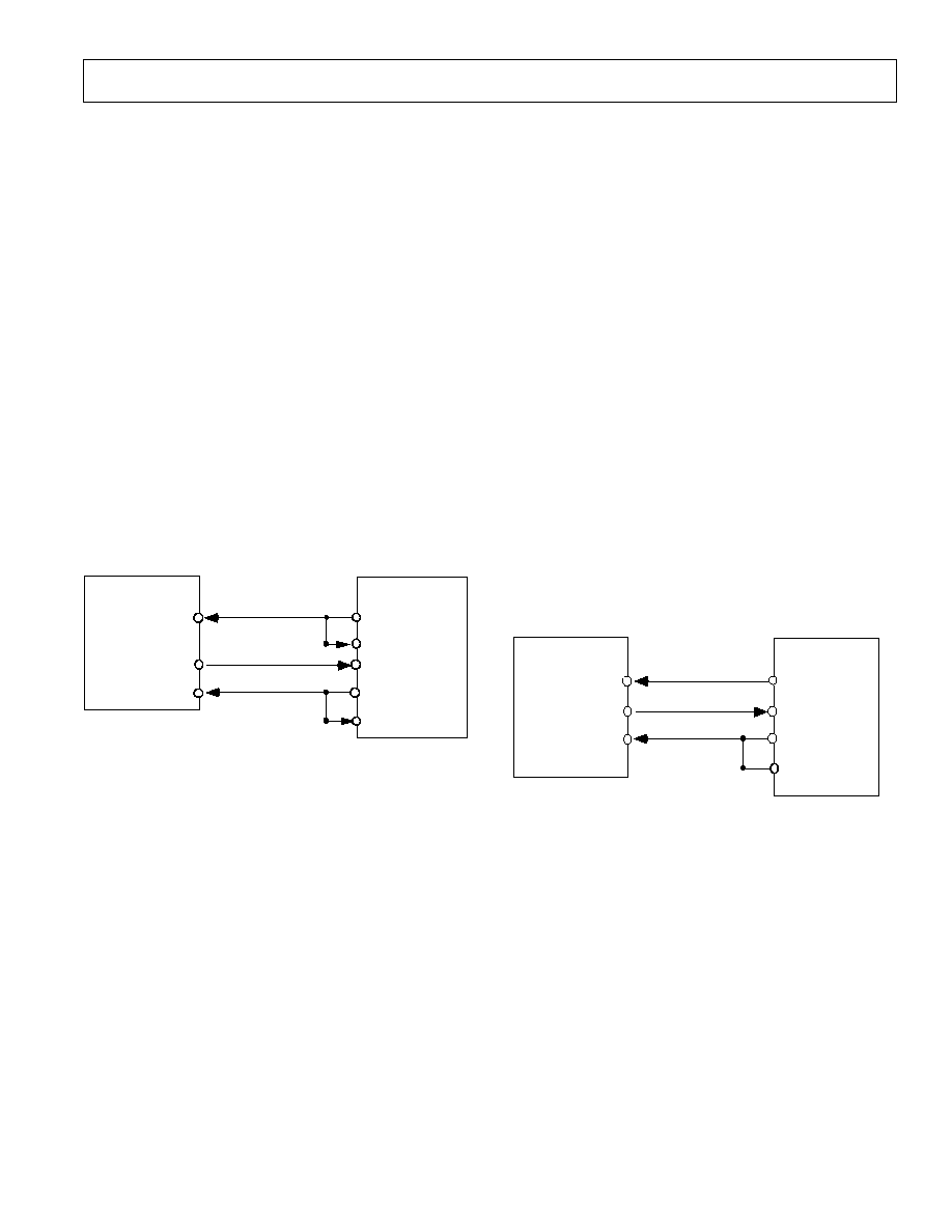
MICROPROCESSOR INTERFACING
The serial interface on the AD7466/AD7467/AD7468
allows the part to be directly connected to a range of many
different microprocessors. This section explains how to
interface the AD7466/AD7467/AD7468 with some of the
more common microcontroller and DSP serial interface
protocols.
AD7466/7/8 to TMS320C5xC54x
The serial interface on the TMS320C5x uses a continuous
serial clock and frame synchronization signals to synchro-
nize the data transfer operations with peripheral devices
like the AD7466/67/68. The
CS input allows easy inter-
facing between the TMS320C5x and the AD7466/67/68
without any glue logic required. The serial port of the
TMS320C5x/C54x is set up to operate in burst mode
with internal CLKX (TX serial clock) and FSX (TX
frame sync). The serial port control register (SPC) must
have the following setup: FO = 0, FSM = 1, MCM = 1
and TXM = 1. The format bit, FO, may be set to 1 to set
the word length to 8-bits, in order to implement the
power-down mode on the AD7466/67/68.
The connection diagram is shown in Figure 18. It should
be noted that for signal processing applications, it is im-
perative that the frame synchronisation signal from the
TMS320C5x/C54x will provide equidistant sampling.
AD7466/7/8 to ADSP21xx
The ADSP21xx family of DSPs are interfaced directly to
the AD7466/67/68 without any glue logic required. The
SPORT control register should be set up as follows:
TFSW = RFSW = 1, Alternate Framing
INVRFS = INVTFS = 1, Active Low Frame Signal
DTYPE = 00, Right Justify Data
SLEN = 1111, 16-Bit Data words
ISCLK = 1, Internal serial clock
TFSR = RFSR = 1, Frame every word
IRFS = 0,
ITFS = 1.
The connection diagram is shown in Figure 19. The
ADSP21xx has the TFS and RFS of the SPORT tied
together, with TFS set as an output and RFS set as an
input. The DSP operates in Alternate Framing Mode and
the SPORT control register is set up as described. The
Frame synchronisation signal generated on the TFS is
tied to
CS and as with all signal processing applications
Figure 18. Interfacing to the TMS320C5x
equidistant sampling is necessary. However, in this ex-
ample, the timer interrupt is used to control the sampling
rate of the ADC and under certain conditions, equidistant
sampling may not be acheived.
The Timer registers etc. are loaded with a value
which will provide an interrupt at the required sample
interval. When an interrupt is received, a value is trans-
mitted with TFS/DT (ADC control word). The TFS is
used to control the RFS and hence the reading of data.
The frequency of the serial clock is set in the SCLKDIV
register. When the instrustion to transmit with TFS is
given, (i.e. AX0=TX0), the state of the SCLK is checked.
The DSP will wait until the SCLK has gone High, Low
and High before transmission will start. If the timer and
SCLK values are chosen such that the instruction to trans-
mit occurs on or near the rising edge of SCLK, then the
data may be transmitted or it may wait until the next clock
edge.
For example, the ADSP2111 has a master clock frequency
of 16MHz. If the SCLKDIV register is loaded with the
value 3 then a SCLK of 2MHz is obtained, and 8 master
clock periods will elapse for every 1 SCLK period. If the
timer registers are loaded with the value 803, then 100.5
SCLKs will occur between interrupts and subsequently
between transmit instructions. This situation will result in
non-equidistant sampling as the transmit instruction is
occuring on a SCLK edge. If the number of SCLKs be-
tween interrupts is a whole integer figure of N then equi-
distant sampling will be implemented by the DSP.
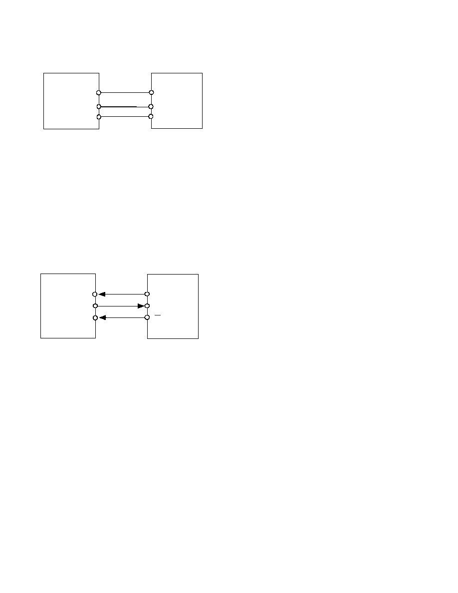
AD7466/67/68 to DSP56xxx
The connection diagram in figure 20 shows how the
AD7466/67/68 can be connected to the SSI (Synchronous
Serial Interface) of the DSP56xxx family of DSPs from
Motorola. The SSI is operated in Synchronous Mode
(SYN bit in CRB =1) with internally generated 1-bit
clock period frame sync for both TX and RX (bits FSL1
=1 and FSL0 =0 in CRB). Set the word length to 16 by
setting bits WL1 =1 and WL0 = 0 in CRA. It should be
noted that for signal processing applications, it is impera-
tive that the frame synchronisation signal from the
DSP56xxx will provide equidistant sampling.
Figure 19. Interfacing to the ADSP-21xx
AD7466/7/8*
SDATA
SCLK
CS
TMS320C5x/C54x*
*Additional Pins omitted for clarity
CLKX
CLKR
DR
FSX
FSR
AD7466/7/8*
SCLK
CS
ADSP21xx*
*Additional Pins omitted for clarity
SCLK
DR
RFS
TFS
SDATA
pecifications
AD7466/AD7467/AD7468
≠14≠
REV. PrC
Figure 20. Interfacing to the DSP56xx
AD7466/67/68 to MC68HC16
The Serial Peripheral Interface (SPI) on the MC68HC16
is configured for Master Mode (MSTR = 1), Clock Po-
larity Bit (CPOL) = 1 and the Clock Phase Bit (CPHA)
= 0. The SPI is configured by writing to the SPI Control
Register (SPCR) - see 68HC16 user manual. The serial
transfer will take place as a 16-bit operation when the
SIZE bit in the SPCR register is set to SIZE = 1. A con-
nection diagram is shown in figure 21.
Figure 21. Interfacing to the MC68HC16
CS
AD7466/7/8*
SCLK
MC68HC16*
SCLK/PMC2
MISO/PMC0
SS/PMC3
*Additional Pins omitted for clarity
SDATA
AD7466/7/8*
SDATA
SCLK
CS
DSP56xxx*
*Additional Pins omitted for clarity
SCK
SRD
SC2
pecifications
AD7466/AD7467/AD7468
≠15≠
REV. PrC
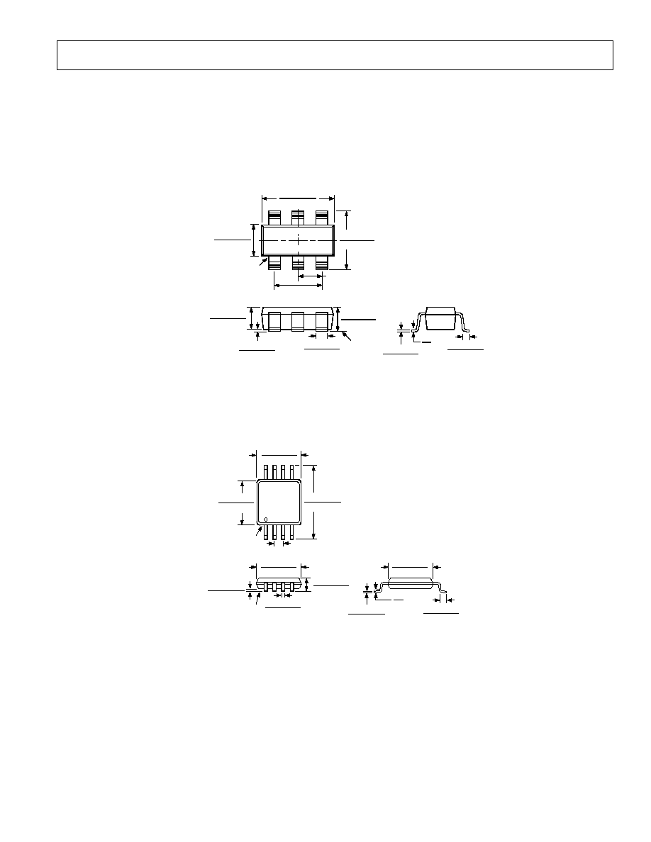
6-lead SOT23 (RT-6)
OUTLINE DIMENSIONS
Dimensions shown in inches and (mm).
0 .12 2 ( 3 .10 )
0 .10 6 ( 2 .70 )
PIN 1
0 .11 8 ( 3 .00 )
0 .09 8 ( 2 .50 )
0 .07 5 ( 1 .90 )
B S C
0 .03 7 (0 .9 5 ) B S C
1
3
4
5
6
2
0 .07 1 ( 1 .80 )
0 .05 9 ( 1 .50 )
0 .00 9 ( 0 .23 )
0 .00 3 ( 0 .08 )
0 .02 2 ( 0 .55 )
0 .01 4 ( 0 .35 )
1 0
∞
0
0 .02 0 ( 0 .50 )
0 .01 0 ( 0 .25 )
0 .00 6 ( 0 .15 )
0 .00 0 ( 0 .00 )
0 .05 1 ( 1 .30 )
0 .03 5 ( 0 .90 )
SE A T IN G
PL A N E
0 .05 7 ( 1 .45 )
0 .03 5 ( 0 .90 )
∞
8
5
4
1
0.122 (3.10)
0.114 (2.90)
0.199 (5.05)
0.187 (4.75)
PIN 1
0.0256 (0.65) BSC
0.122 (3.10)
0.114 (2.90)
SEA TIN G
PLAN E
0.006 (0.15)
0.002 (0.05)
0.018 (0.46)
0.008 (0.20)
0.043 (1.09)
0.037 (0.94)
0.120 (3.05)
0.112 (2.84)
0.011 (0.28)
0.003 (0.08)
0.028 (0.71)
0.016 (0.41)
33∞
27∞
0.120 (3.05)
0.112 (2.84)
8-lead microSOIC (RM-8)
pecifications