REV. A
Information furnished by Analog Devices is believed to be accurate and
reliable. However, no responsibility is assumed by Analog Devices for its
use, nor for any infringements of patents or other rights of third parties
which may result from its use. No license is granted by implication or
otherwise under any patent or patent rights of Analog Devices.
a
CMOS Dual 8-Bit
Buffered Multiplying DAC
AD7628
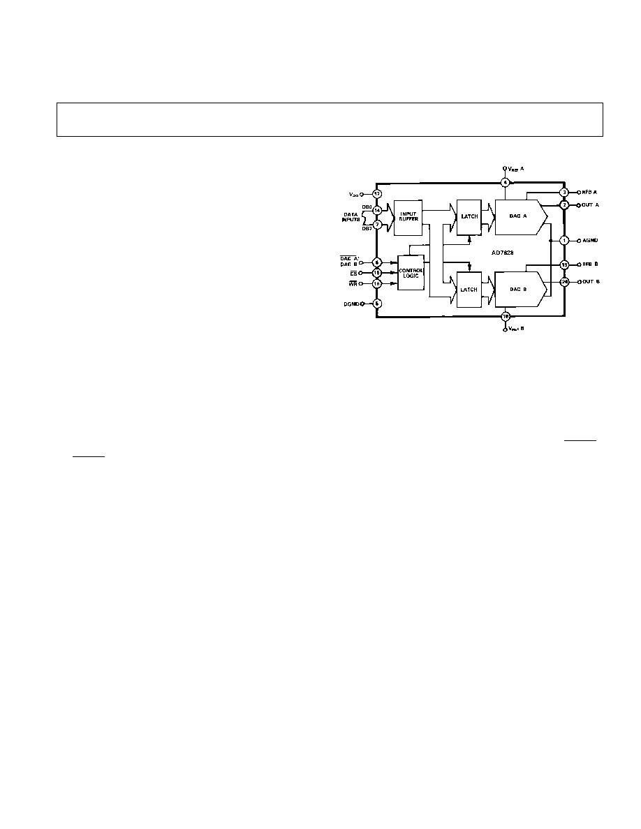
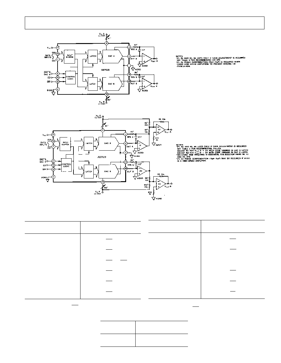
FUNCTIONAL BLOCK DIAGRAM
GENERAL DESCRIPTION
The AD7628 is a monolithic dual 8-bit digital/analog converter
featuring excellent DAC-to-DAC matching. It is available in
small 0.3" wide 20-pin DIPs and in 20-terminal surface mount
packages.
Separate on-chip latches are provided for each DAC to allow
easy microprocessor interface.
Data is transferred into either of the two DAC data latches via a
common 8-bit TTL/CMOS compatible input port. Control in-
put
DAC A/DAC B determines which DAC is to be loaded.
The AD7628's load cycle is similar to the write cycle of a ran-
dom access memory, and the device is bus compatible with most
8-bit microprocessors, including 6502, 6809, 8085, Z80.
The device operates from a +12 V to +15 V power supply and is
TTL-compatible over this range. Power dissipation is a low
20 mW.
Both DACs offer excellent four quadrant multiplication charac-
teristics with a separate reference input and feedback resistor for
each DAC.
PRODUCT HIGHLIGHTS
1. DAC to DAC matching: since both of the AD7628 DACs
are fabricated at the same time on the same chip, precise
matching and tracking between DAC A and DAC B is inher-
ent. The AD7628's matched CMOS DACs make a whole
new range of applications circuits possible, particularly in the
audio, graphics and process control areas.
2. Small package size: combining the inputs to the on-chip
DAC latches into a common data bus and adding a
DAC A/
DAC B select line has allowed the AD7628 to be packaged in
a small 20-pin 0.3" wide DIP, 20-pin SOIC, 20-terminal
PLCC and 20-terminal LCC.
3. TTL-Compatibility: All digital inputs are TTL-compatible
over a +12 V to +15 V power supply range.
FEATURES
On-Chip Latches for Both DACs
+12 V to +15 V Operation
DACs Matched to 1%
Four Quadrant Multiplication
TTL/CMOS Compatible from +12 V to +15 V
Latch Free (Protection Schottkys not Required)
APPLICATIONS
Disk Drives
Programmable Filters
X-Y Graphics
Gain/Attenuation
One Technology Way, P.O. Box 9106, Norwood, MA 02062-9106, U.S.A.
Tel: 617/329-4700
World Wide Web Site: http://www.analog.com
Fax: 617/326-8703
� Analog Devices, Inc., 1996
T
A
= �40 C
T
A
= �55 C
Parameter
T
A
= +25 C
1
to +85 C
to +125 C
1
Units
Test Conditions/Comments
STATIC PERFORMANCE
2
Resolution
8
8
8
Bits
Relative Accuracy
�
1/2
�
1/2
�
1/2
LSB max
This is an Endpoint Linearity Specification
Differential Nonlinearity
�
1
�
1
�
l
LSB max
All Grades Guaranteed Monotonic Over
Full Operating Temperature Range
Gain Error
�
2
�
3
�
3
LSB max
Measured Using Internal RFB A and RFB B.
Both DAC Latches Loaded with 11111111.
Gain Error is Adjustable Using Circuits
of Figures 4 and 5.
Gain Temperature Coefficient
3
Gain/
Temperature
�
0.0035
�
0.0035
%/
�
C max
Output Leakage Current
OUT A (Pin 2)
�
50
�
200
�
200
nA max
DAC Latches Loaded with 00000000
OUT B (Pin 20)
�
50
�
200
�
200
nA max
Input Resistance (V
REF
A, V
REF
B)
8
8
8
k
min
Input Resistance TC = �300 ppm/
�
C, Typical
15
15
15
k
max
Input Resistance is 11 k
V
REF
A/V
REF
B Input Resistance
Match
�
1
�
1
�
1
% max
DIGITAL INPUTS
4
Input High Voltage (V
IH
)
2.4
2.4
2.4
V min
Input Low Voltage (V
IL
)
0.8
0.8
0.8
V max
Input Current (I
IN
)
�
1
�
10
�
10
�
A max
V
IN
= 0 or V
DD
Input Capacitance
DB0�DB7
10
10
10
pF max
WR, CS, DACA/DACB
15
15
15
pF max
SWITCHING CHARACTERISTICS
3
See Timing Diagram
Chip Select to Write Set Up Time (t
CS
)
160
160
210
ns min
Chip Select to Write Hold Time (t
CH
)
10
10
10
ns min
DAC Select to Write Set Up Time (t
AS
)
160
160
210
ns min
DAC Select to Write Hold Time (t
AH
)
10
10
10
ns min
Data Valid to Write Set Up Time (t
DS
)
160
160
210
ns min
Data Valid to Write Hold Time (t
DH
)
10
10
10
ns min
Write Pulse Width (t
WR
)
150
170
210
ns min
POWER SUPPLY
See Figure 3
I
DD
, K Grade
2
2
mA
All Digital Inputs V
IL
or V
IH
B, T Grades
2
2.5
2.5
mA
All Digital Inputs V
IL
or V
IH
All Grades
100
500
500
�
A
All Digital Inputs 0 V or V
DD
Specifications subject to change without notice.
AC PERFORMANCE CHARACTERISTICS
T
A
= �40 C
T
A
= �55 C
Parameter
T
A
= +25 C
1
to +85 C
1
to +125
C
1
Units
Test Conditions/Comments
DC SUPPLY REJECTION
(
GAIN/
V
DD
)
0.01
0.02
0.02
% per % max
V
DD
=
�
5%
CURRENT SETTLING TIME
350
400
400
ns max
To 1/2 LSB OutA/OutB Load = 100
.
WR = CS = 0 V.
DB0�DB7 = 0 V to V
DD
or V
DD
to 0 V
DIGITAL-TO-ANALOG GLITCH
IMPULSE
330
nV sec typ
For Code Transition 00000000 to 11111111
OUTPUT CAPACITANCE
C
OUT
A
25
25
25
pF max
DAC Latches Loaded with 00000000
C
OUT
B
25
25
25
pF max
C
OUT
A
60
60
60
pF max
DAC Latches Loaded with 11111111
C
OUT
B
60
60
60
pF max
AC FEEDTHROUGH
V
REF
A to OUT A
�70
�65
�65
dB max
V
REF
A, V
REF
B = 20 V p-p Sine Wave
V
REF
B to OUT B
�70
�65
�65
dB max
@ 10 kHz
CHANNEL-TO-CHANNEL ISOLATION
Both DAC Latches Loaded with 11111111.
V
REF
A to OUT B
�80
dB typ
V
REF
A = 20 V p-p Sine Wave @ 10 kHz
V
REF
B = 0 V See Figure 6.
V
REF
B to OUTA
�80
dB typ
V
REF
B = 20 V p-p Sine Wave @ 10 kHz
V
REF
A = 0 V See Figure 6.
DIGITAL CROSSTALK
60
nV sec typ
Measured for Code Transition 00000000
to 11111111
HARMONIC DISTORTION
�85
dB typ
V
IN
= 6 V rms @ 1 kHz
NOTES
1
Temperature Ranges are K Version; �40
�
C to +85
�
C; B Version; �40
�
C to +85
�
C; T Version; �55
�
C to +125
�
C.
2
Specification applies to both DACs in AD7628.
3
Guaranteed by design but not production tested.
4
Logic inputs are MOS Gates. Typical input current (+25
�
C) is less than 1 nA.
Specifications subject to change without notice.
REV. A
�2�
AD7628�SPECIFICATIONS
(V
DD
= +10.8 V to +15.75 V, V
REF
A = V
REF
B = +10 V; OUT A = OUT B = 0 V unless
otherwise noted)
These characteristics are included for Design Guidance only and are not
subject to test. V
DD
= +10.8 V to +15.75 V. (Measured Using Recommended PC Board Layout (Figure 7) and AD644 as Output Amplifiers)
AD7628
�3�
REV. A
ABSOLUTE MAXIMUM RATINGS
(T
A
= +25
�
C unless otherwise noted)
V
DD
to AGND . . . . . . . . . . . . . . . . . . . . . . . . . . . . 0 V, +17 V
V
DD
to DGND . . . . . . . . . . . . . . . . . . . . . . . . . . . . 0 V, +17 V
AGND to DGND . . . . . . . . . . . . . . . . . . . . . . . . V
DD
+ 0.3 V
DGND to AGND . . . . . . . . . . . . . . . . . . . . . . . . V
DD
+ 0.3 V
Digital Input Voltage to DGND . . . . . . �0.3 V, V
DD
+ 0.3 V
V
PIN2
, V
PIN20
to AGND . . . . . . . . . . . . . . �0.3 V, V
DD
+ 0.3 V
V
REF
A, V
REF
B to AGND . . . . . . . . . . . . . . . . . . . . . . .
�
25 V
V
RFB
A, V
RFB
B to AGND . . . . . . . . . . . . . . . . . . . . . . .
�
25 V
Power Dissipation (Any Package) to +75
�
C . . . . . . . . 450 mW
Derates above +75
�
C by . . . . . . . . . . . . . . . . . . . 6 mW/
�
C
Operating Temperature Range
Commercial (K) Grades . . . . . . . . . . . . . . . �40
�
C to +85
�
C
Industrial (B) Grades . . . . . . . . . . . . . . . . . �40
�
C to +85
�
C
Extended (T) Grades . . . . . . . . . . . . . . . . �55
�
C to +125
�
C
Storage Temperature . . . . . . . . . . . . . . . . . �65
�
C to +150
�
C
Lead Temperature (Soldering, 10 sec) . . . . . . . . . . . . +300
�
C
ORDERING GUIDE
Temperature
Relative
Gain
Package
Model
1
Range
Accuracy Error
Option
2
AD7628KN
�40
�
C to +85
�
C
�
1/2 LSB
�
2 LSB
N-20
AD7628KP
�40
�
C to +85
�
C
�
1/2 LSB
�
2 LSB
P-20A
AD7628KR
�40
�
C to +85
�
C
�
1/2 LSB
�
2 LSB
R-20
AD7628BQ
�40
�
C to +85
�
C
�
1/2 LSB
�
2 LSB
Q-20
AD7628TQ
�55
�
C to +125
�
C
�
1/2 LSB
�
2 LSB
Q-20
AD7628TE
�55
�
C to +125
�
C
�
1/2 LSB
�
2 LSB
E-20A
NOTES
1
To order MIL-STD-883, Class B process parts, add /883B to part number.
Contact your local sales office for military data sheet.
2
E = Leadless Ceramic Chip Carrier; N = Plastic DIP; P = Plastic Leaded Chip
Carrier; Q = Cerdip; R = SOIC.
WARNING!
ESD SENSITIVE DEVICE
CAUTION
ESD (electrostatic discharge) sensitive device. Electrostatic charges as high as 4000 V readily
accumulate on the human body and test equipment and can discharge without detection.
Although the AD7628 features proprietary ESD protection circuitry, permanent damage may
occur on devices subjected to high energy electrostatic discharges. Therefore, proper ESD
precautions are recommended to avoid performance degradation or loss of functionality.
TERMINOLOGY
Relative Accuracy:
Relative accuracy or endpoint nonlinearity is a measure of the
maximum deviation from a straight line passing through the
endpoints of the DAC transfer function. It is measured after ad-
justing for zero and full-scale, and is normally expressed in
LSBs or as a percentage of full-scale reading.
Differential Nonlinearity:
Differential nonlinearity is the difference between the measured
change and the ideal 1 LSB change between any two adjacent
codes. A specified differential nonlinearity of
�
1 LSB max over
the operating temperature range ensures monotonicity.
Gain Error:
Gain error is a measure of the output error between an ideal
DAC and the actual device output. It is measured with all 1s in
the DAC latches after offset error has been adjusted out. Gain
error of both DACs is adjustable to zero with external resistance.
Output Capacitance:
Capacitance from OUT A or OUT B to AGND.
Digital-to-Analog Glitch Impulse:
The amount of charge injected from the digital inputs to the
analog output when the inputs change state. This is normally
specified as the area of the glitch in either pA-secs or nV-secs,
depending upon whether the glitch is measured as a current or
voltage signal. Glitch impulse is measured with V
REF
A, V
REF
B
= AGND.
Channel-to-Channel Isolation:
The proportion of input signal from one DAC's reference input
that appears at the output of the other DAC, expressed as a
ratio in dB.
Digital Crosstalk:
The glitch energy transferred to the output of one converter due
to a change in digital input code to the other converter. Speci-
fied in nV secs.
PIN CONFIGURATIONS
DIP, SOIC
AGND
OUT A
OUT B
RFB B
DGND
DAC A/DAC B
(MSB) DB7
WR
CS
DB0 (LSB)
RFB A
V
REF
A
V
REF
B
V
DD
DB6
DB1
DB5
DB2
DB4
DB3
1
2
20
19
5
6
7
16
15
14
3
4
18
17
8
13
9
12
10
11
TOP VIEW
(Not to Scale)
AD7628
LCCC
V
REF
A
DGND
DB6
DAC A /DAC B
DB7 (MSB)
OUT A
RFB B
AGND
OUT B
DB5
DB4
DB1
DB3
DB2
V
REF
B
V
DD
DB0 (LSB)
WR
CS
19
3
1
2
20
4
5
8
6
7
12 13
9
11
10
18
17
14
16
15
TOP VIEW
(Not to Scale)
AD7628
RFB A
PLCC
V
REF
A
DGND
DB6
DAC A/DAC B
DB7 (MSB)
RFB A
OUT A
RFB B
AGND
OUT B
DB5
DB4
DB1
DB3
DB2
V
REF
B
V
DD
DB0 (LSB)
WR
CS
19
3
1
2
20
4
5
8
6
7
12 13
9
11
10
18
17
14
16
15
TOP VIEW
(Not to Scale)
AD7628
AD7628
�4�
REV. A
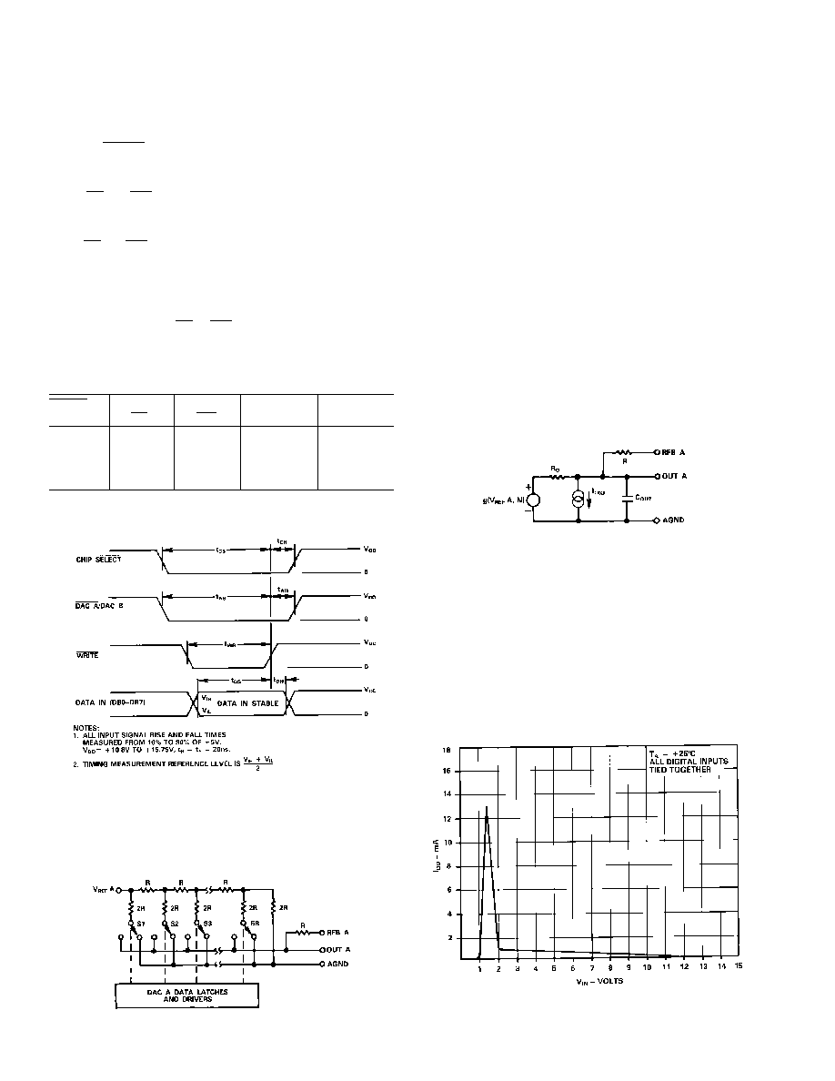
INTERFACE LOGIC INFORMATION
DAC Selection
Both DAC latches share a common 8-bit input port. The con-
trol input
DAC A/DAC B selects which DAC can accept data
from the input port.
Mode Selection
Inputs
CS and WR control the operating mode of the selected
DAC. See Mode Selection Table below.
Write Mode
When
CS and WR are both low, the selected DAC is in the write
mode. The input data latches of the selected DAC are transpar-
ent and its analog output responds to activity on DB0�DB7.
Hold Mode
The selected DAC latch retains the data that was present on
DB0�DB7 just prior to
CS or WR assuming a high state. Both
analog outputs remain at the values corresponding to the data in
their respective latches.
Mode Selection Table
DAC A/
DAC B
CS
WR
DAC A
DAC B
L
L
L
WRITE
HOLD
H
L
L
HOLD
WRITE
X
H
X
HOLD
HOLD
X
X
H
HOLD
HOLD
L = Low State, H = High State, X = Don't Care
WRITE CYCLE TIMING DIAGRAM
CIRCUIT INFORMATION--D/A SECTION
The AD7628 contains two identical 8-bit multiplying D/A con-
verters, DAC A and DAC B. Each DAC consists of a highly
stable thin film R-2R ladder and eight N-channel current steering
switches. A simplified D/A circuit for DAC A is shown in Figure
1. An inverted R-2R ladder structure is used; that is, binary
Figure 1. Simplified Functional Circuit for DAC A
weighted currents are switched between the DAC output and
AGND, thus maintaining fixed currents in each ladder leg inde-
pendent of switch state.
EQUIVALENT CIRCUIT ANALYSIS
Figure 2 shows an approximate equivalent circuit for one of
the AD7628's D/A converters, in this case DAC A. A similar
equivalent circuit can be drawn for DAC B. Note that AGND
(Pin 1) is common for both DAC A and DAC B.
The current source I
LEAKAGE
is composed of surface and junc-
tion leakages and, as with most semiconductor devices, approxi-
mately doubles every 10
�
C. The resistor Ro, as shown in Fig-
ure 2, is the equivalent output resistance of the device, which
varies with input code (excluding all 0s code) from 0.8R to 2R.
R is typically 11 k
. C
OUT
is the capacitance due to the N-channel
switches and varies from about 50 pF to 120 pF, depending on
the digital input. g(V
REF
A, N) is the Thevenin equivalent volt-
age generator due to the reference input voltage V
REF
A and the
transfer function of the R-2R ladder.
For further information on CMOS multiplying D/A converters,
refer to "CMOS DAC Application Guide, 2ND Edition" avail-
able from Analog Devices, Publication Number G872a�15�4/86.
Figure 2. Equivalent Analog Output Circuit of DAC A
CIRCUIT INFORMATION�DIGITAL SECTION
The input buffers are simple CMOS level-shifters designed so
that when the AD7628 is operated with V
DD
from 10.8 V to
15.75 V, the buffer converts TTL input levels (2.4 V and 0.8 V)
into CMOS logic levels. When V
IN
is in the region of 1.0 volt to
2.0 volts, the input buffers operate in their linear region and
pass a quiescent current (see Figure 3). To minimize power sup-
ply currents, it is recommended that the digital input voltages be as
close to the supply rails (V
DD
and DGND) as practicably possible.
The AD7628 may be operated with any supply voltage in the
range 10.8
V
DD
15.75 volts.
Figure 3. Typical Plot of Supply Current, I
DD
vs. Logic
Input Voltage V
IN
to V
DD
= +15 V
AD7628
�5�
REV. A
Table I. Unipolar Binary Code Table
DAC Latch Contents
Analog Output
MSB
LSB
(DAC A or DAC B)
1 1 1 1 1 1 1 1
�V
IN
255
256
1 0 0 0 0 0 0 1
�V
IN
129
256
1 0 0 0 0 0 0 0
�V
IN
128
256
=
�
V
IN
2
0 1 1 1 1 1 1 1
�V
IN
127
256
0 0 0 0 0 0 0 1
�V
IN
1
256
0 0 0 0 0 0 0 0
�V
IN
0
256
=
0
NOTE: 1 LSB = (2
�8
)(V
IN
) =
1
256
V
IN
( )
Figure 4. Dual DAC Unipolar Binary Operation (2 Quadrant Multiplication). See Table I.
Figure 5. Dual DAC Bipolar Operation (4 Quadrant Multiplication). See Table II.
Table II. Bipolar (Offset Binary) Code Table
DAC Latch Contents
Analog Output
MSB
LSB
(DAC A or DAC B)
1 1 1 1 1 1 1 1
+
V
IN
127
128
1 0 0 0 0 0 0 1
+
V
IN
1
128
1 0 0 0 0 0 0 0
0
0 1 1 1 1 1 1 1
�V
IN
1
128
0 0 0 0 0 0 0 1
�V
IN
127
128
0 0 0 0 0 0 0 0
�V
IN
128
128
NOTE: 1 LSB = (2
�7
)(V
IN
) =
1
128
V
IN
( )
Table III. Recommended Trim Resistor Values
Trim
Resistor
K/B/T
R1; R3
500
R2; R4
150
AD7628
�6�
REV. A
APPLICATIONS INFORMATION
Application Hints
To ensure system performance consistent with AD7628 specifi-
cations, careful attention must be given to the following points:
1. GENERAL GROUND MANAGEMENT: AC or transient
voltages between the AD7628 AGND and DGND can cause
noise injection into the analog output. The simplest method
of ensuring that voltages at AGND and DGND are equal is
to tie AGND and DGND together at the AD7628. In more
omplex systems where the AGND�DGND intertie is on the
backplane, it is recommended that diodes be connected in
inverse parallel between the AD7628 AGND and DGND
pins (1N914 or equivalent).
2. OUTPUT AMPLIFIER OFFSET: CMOS DACs exhibit a
code-dependent output resistance which, in turn, causes a
code-dependent amplifier noise gain. The effect is a code-
dependent differential nonlinearity term at the amplifier
output that depends on V
OS
(V
OS
is amplifier input offset
voltage). This differential nonlinearity term adds to the R/2R
differential nonlinearity. To maintain monotonic operation, it
is recommended that amplifier V
OS
be no greater than 10% of
1 LSB over the temperature range of interest.
3. HIGH FREQUENCY CONSIDERATIONS: The output
capacitance of a CMOS DAC works in conjunction with the
amplifier feedback resistance to add a pole to the open loop
response. This can cause ringing or oscillation. Stability can
be restored by adding a phase compensation capacitor in
parallel with the feedback resistor.
DYNAMIC PERFORMANCE
The dynamic performance of the two DACs in the AD7628 will
depend on the gain and phase characteristics of the output am-
plifiers, together with the optimum choice of the PC board lay-
out and decoupling components. Figure 6 shows the relationship
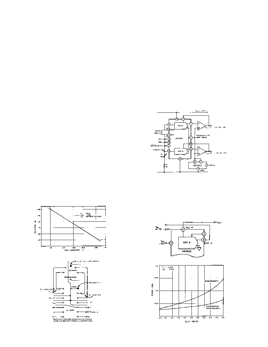
between input frequency and channel-to-channel isolation.
Figure 6. Channel-to-Channel Isolation
Figure 7. Suggested PC Board Layout for AD7628 with
AD644 Dual Op Amp
Figure 7 shows a printed circuit layout for the AD7628 and the
AD644 dual op amp, which minimizes feedthrough and crosstalk.
SINGLE SUPPLY APPLICATIONS
The AD7628 DAC R-2R ladder termination resistors are con-
nected to AGND within the device. This arrangement is par-
ticularly convenient for single supply operation because AGND
may be biased at any voltage between DGND and V
DD
. Figure
8 shows a circuit that provides two +5 V to +8 V analog outputs
by biasing AGND +5 V up from DGND. The two DAC refer-
ence inputs are tied together and a reference input voltage is ob-
tained without a buffer amplifier by making use of the constant
and matched impedances of the DAC A and DAC B reference
inputs. Current flows through the two DAC R-2R ladders into
R1, and R1 is adjusted until the V
REF
A and V
REF
B inputs are
at +2 V. The two analog output voltages range from +5 V to
+8 V for DAC codes 00000000 to l l l l l l l l .
Figure 8. AD7628 Single Supply Operation
Figure 9 shows DAC A of the AD7628 connected in a positive
reference, voltage switching mode. This configuration is useful
because V
OUT
is the same polarity as V
IN
, allowing single supply
operation. However, to retain specified linearity, V
IN
must be in
the range 0 V to +2.5 V and the output buffered or loaded with
a high impedance (see Figure 10). Note that the input voltage is
connected to the DAC OUT A, and the output voltage is taken
from the DAC V
REF
A pin.
Figure 9. AD7628 Single Supply, Voltage Switching Mode
Figure 10. Typical AD7628 Performance in Single Supply
Voltage Switching Mode
AD7628
�7�
REV. A
MICROPROCESSOR INTERFACE
Figure 11. AD7628 Dual DAC to 6800 CPU Interface
PROGRAMMABLE WINDOW COMPARATOR
Figure 13. Digitally Programmable Window Comparator
(Upper and Lower Limit Detector)
PROGRAMMABLE STATE VARIABLE FILTER
Figure 12. AD7628 Dual DAC to 8085 CPU Interface
In the circuit of Figure 13, the AD7628 is used to implement a
programmable window comparator. DACs A and B are loaded
with the required upper and lower voltage limits for the test,
respectively. If the test input is not within the programmed lim-
its, the pass/fail output will indicate a fail (logic zero).
In this state, variable or universal filter configuration (Figure
14) for DACs A1 and B1 control the gain and Q of the filter
characteristic, while DACs A2 and B2 control the cutoff fre-
quency, f
C
. DACs A2 and B2 must track accurately for the simple
expression for f
C
to hold. This is readily accomplished by the
AD7628. Op amps are 2
�
AD644. C3 compensates for the
effects of op amp gain-bandwidth limitations.
The filter provides low pass, high pass and band pass outputs
and is ideally suited for applications where microprocessor con-
trol of filter parameters is required, e.g., equalizer, tone con-
trols, etc.
Programmable range for component values shown is f
C
= 0 kHz
to 15 kHz and Q = 0.3 to 4.5.
Figure 14. Digitally Controlled State Variable Filter
CIRCUIT EQUATIONS
C
1
= C
2
, R
1
= R
2
, R
4
= R
5
f
C
=
1
2
R
1
C
1
Q =
R
3
R
4
.
R
F
R
FBB1
A
O
= �
R
F
R
S
NOTE
DAC equivalent resistance equals
256
�
DAC Ladder resistance
(
)
DAC Digital Code
AD7628
�8�
REV. A
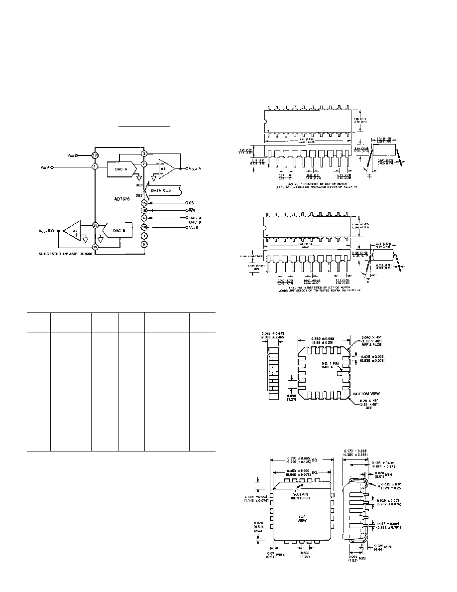
MECHANICAL INFORMATION
OUTLINE DIMENSIONS
Dimensions shown in inches and (mm).
C1029a�8�3/88
PRINTED IN U.S.A.
DIGITALLY CONTROLLED DUAL
TELEPHONE ATTENUATOR
In this configuration, the AD7628 functions as a 2-channel
digitally controlled attenuator; ideal for stereo audio and tele-
phone signal level control applications. Table IV gives input
codes vs. attenuation for a 0 dB to 15.5 dB range.
Input Code = 256
�
10 exp
-
Attenuation, dB
20
Figure 15. Digitally Controlled Dual Telephone Attenuator
Table IV. Attenuation vs. DAC A, DAC B Code for the
Circuit of Figure 15
DAC Input
Code in
DAC Input
Code in
Attn. dB Code
Decimal Attn. dB
Code
Decimal
0.
0
1 1 1 1 1 1 1 1
255
8.0
0 1 1 0 0 1 1 0
102
0.5
1 1 1 1 0 0 1 0
242
8.5
0 1 1 0 0 0 0 0
96
1.0
1 1 1 0 0 1 0 0
228
9.0
0 1 0 1 1 0 1 1
91
1.5
1 1 0 1 0 1 1 1
215
9.5
0 1 0 1 0 1 1 0
86
2.0
1 1 0 0 1 0 1 1
203
10.0
0 1 0 1 0 0 0 1
81
2.5
1 1 0 0 0 0 0 0
192
10.5
0 1 0 0 1 1 0 0
76
3.0
1 0 1 1 0 1 0 1
181
11.0
0 1 0 0 1 0 0 0
72
3.5
1 0 1 0 1 0 1 1
171
11.5
0 1 0 0 0 1 0 0
68
4.0
1 0 1 0 0 0 1 0
162
12.0
0 1 0 0 0 0 0 0
64
4.5
1 0 0 1 1 0 0 0
152
12.5
0 0 1 1 1 1 0 1
61
5.0
1 0 0 1 0 0 0 0
144
13.0
0 0 1 1 1 0 0 1
57
5.5
1 0 0 0 1 0 0 0
136
13.5
0 0 1 1 0 1 1 0
54
6.0
1 0 0 0 0 0 0 0
128
14.0
0 0 1 1 0 0 1
51
6.5
0 1 1 1 0 0 1
121
14.5
0 0 1 1 0 0 0 0
48
7.0
0 1 1 1 0 0 1 0
114
15.0
0 0 1 0 1 1 1 0
46
7.5
0 1 1 0 1 1 0 0
108
15.5
0 0 1 0 1 0 1 1
43
20-Pin Cerdip (Q Suffix)
20-Pin Plastic DIP (N Suffix)
20-Terminal
Leadless Chip
Carrier (E Suffix)
20-Terminal
Plastic Leaded
Chip Carrier (P Suffix)