Touch Screen Controller
AD7877
Rev. A
Information furnished by Analog Devices is believed to be accurate and reliable.
However, no responsibility is assumed by Analog Devices for its use, nor for any
infringements of patents or other rights of third parties that may result from its use.
Specifications subject to change without notice. No license is granted by implication
or otherwise under any patent or patent rights of Analog Devices. Trademarks and
registered trademarks are the property of their respective owners.
One Technology Way, P.O. Box 9106, Norwood, MA 02062-9106, U.S.A.
Tel: 781.329.4700
www.analog.com
Fax: 781.326.8703
© 2004 Analog Devices, Inc. All rights reserved.
FEATURES
4-wire touch screen interface
LCD noise reduction feature (STOPACQ pin)
Automatic conversion sequencer and timer
User-programmable conversion parameters
On-chip temperature sensor: -40∞C to +85∞C
On-chip 2.5 V reference
On-chip 8-bit DAC
3 auxiliary analog inputs
1 dedicated and 3 optional GPIOs
2 direct battery measurement channels (0.5 V to 5 V)
3 interrupt outputs
Touch-pressure measurement
Wake up on touch function
Specified throughput rate of 125 kSPS
Single supply, V
CC
of 2.7 V to 5.25 V
Separate V
DRIVE
level for serial interface
Shutdown mode: 1 µA maximum
32-lead LFCSP 5 mm x 5 mm package
APPLICATIONS
Personal digital assistants
Smart hand-held devices
Touch screen monitors
Point-of-sale terminals
Medical devices
Cell phones
Pagers
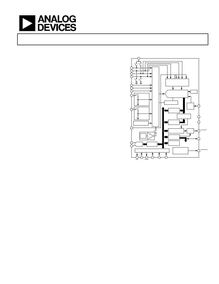
FUNCTIONAL BLOCK DIAGRAM
19
DIN
26
DCLK
27
DOUT
28
V
DRIVE
18
CS
23
DAV
CONTROL LOGIC AND SERIAL PORT
DAC
REGISTER
CONTROL
REGISTERS
GPIO
REGISTERS
ALERT STATUS/
MASK REGISTER
LIMIT
REGISTERS
LIMIT
COMPARATOR
RESULTS
REGISTERS
SEQUENCER
8-BIT
DAC
29
ARNG
30
AOUT
4
AUX3/GPIO3
5
AUX2/GPIO2
6
AUX1/GPIO1
31
V
REF
PEN INTERRUPT
AND WAKE-UP
ON TOUCH
17
PENIRQ
ALERT
LOGIC
22
ALERT
STOP
ACQ
LOGIC
20
STOPACQ
14
AGND
15
DGND
21
GPIO4
2.5V
REF
BUF
TO
GPIO1-3
ADC DATA
12-BIT SUCCESSIVE
APPROXIMATION ADC
WITH TRACK-AND-HOLD
CLOCK
9 TO 1
I/P
MUX
TEMPERATURE
SENSOR
2
BAT2
BATTERY
MONITOR
3
BAT1
BATTERY
MONITOR
11
Y≠
13
Y+
10
X≠
12
X+
7
V
CC
REF≠
IN
REF+
DUAL 3-1
MUX
X≠ Y≠ GND X+ Y+ V
REF
AD7877
03796-001
Figure 1.
GENERAL DESCRIPTION
The AD7877 is a 12-bit successive approximation ADC with a
synchronous serial interface and low on resistance switches for
driving touch screens. The AD7877 operates from a single 2.7 V
to 5.25 V power supply (functional operation to 2.2V), and
features throughput rates of 125 kSPS. The AD7877 features
direct battery measurement on two inputs, temperature and
touch-pressure measurement.
The AD7877 also has an on-board reference of 2.5 V. When not
in use, it can be shut down to conserve power. An external
reference can also be applied and can be varied from 1 V to
+V
CC
, while the analog input range is from 0 V to V
REF
. The
device includes a shutdown mode, which reduces its current
consumption to less than 1 µA.
To reduce the effects of noise from LCDs, the acquisition phase
of the on-board ADC can be controlled via the STOPACQ pin.
User-programmable conversion controls include variable
acquisition time and first conversion delay. Up to 16 averages
can be taken per conversion. There is also an on-board DAC for
LCD backlight or contrast control. The AD7877 can run in
either slave or master mode, using a conversion sequencer and
timer. It is ideal for battery-powered systems such as personal
digital assistants with resistive touch screens and other portable
equipment.
The part is available in a 32-lead lead frame chip scale package
(LFCSP).

AD7877
Rev. A | Page 2 of 44
TABLE OF CONTENTS
Specifications..................................................................................... 3
Timing Specifications....................................................................... 5
Absolute Maximum Ratings............................................................ 6
ESD Caution.................................................................................. 6
Pin Configuration and Function Descriptions............................. 7
Terminology ...................................................................................... 9
Typical Performance Characteristics ........................................... 10
Circuit Information ........................................................................ 14
Touch Screen Principles ............................................................ 14
Measuring Touch Screen Inputs ............................................... 15
Touch-Pressure Measurement .................................................. 16
STOPACQ Pin ............................................................................ 16
Temperature Measurement ....................................................... 17
Battery Measurement................................................................. 18
Auxiliary Inputs .......................................................................... 19
Limit Comparison ...................................................................... 19
Control Registers ............................................................................ 20
Control Register 1....................................................................... 20
Control Register 2....................................................................... 21
Sequencer Registers ................................................................... 22
Interrupts..................................................................................... 24
Syncronizing the AD7877 to the Host CPU ........................... 25
8-Bit DAC ........................................................................................ 26
Serial Interface ................................................................................ 28
Writing Data ............................................................................... 28
Write Timing............................................................................... 29
Reading Data............................................................................... 29
V
DRIVE
Pin..................................................................................... 29
General-Purpose I/O Pins............................................................. 30
GPIO Configuration .................................................................. 30
Grounding and LayouT ................................................................. 32
PCB Design Guidelines for Chip Scale Packages................... 32
Register Maps.................................................................................. 33
Detailed Register Descriptions ..................................................... 35
GPIO Registers ........................................................................... 41
Outline Dimensions ....................................................................... 43
Ordering Guide .......................................................................... 43
REVISION HISTORY
11/04--Changed from Rev. 0 to Rev. A
Changes to Absolute Maximum Ratings ...................................... 6
Changes to Figure 4.......................................................................... 7
Changes to Table 4............................................................................ 7
Changes to Grounding and Layout section ................................ 32
Changes to Figure 42...................................................................... 32
Changes to Ordering Guide .......................................................... 43
7/04--Revision 0: Initial Version

AD7877
Rev. A | Page 3 of 44
SPECIFICATIONS
V
CC
= 2.7 V to 3.6 V, V
REF
= 2.5 V internal or external, f
DCLK
= 2 MHz, T
A
= -40∞C to +85∞C, unless otherwise noted.
Table 1.
Parameter
Min
Typ
Max
Unit
Test Conditions/Comments
ADC
DC
ACCURACY
Resolution
12
Bits
No Missing Codes
11
12
Bits
Integral Nonlinearity
1
±2
LSB
LSB size = 610 µV
Differential Nonlinearity
1
-0.99/+2
LSB
LSB size = 610 µV
Offset Error
1
±2
±6
LSB
V
CC
= 2.7 V
Gain Error
1
±4
LSB
External reference
Noise
70
µV rms
Power Supply Rejection
70
dB
Internal Clock Ffrequency
2
MHz
SWITCH
DRIVERS
On Resistance
1
Y+, X+
14
Y-, X-
14
ANALOG INPUTS
Input Voltage Ranges
0
V
REF
V
DC Leakage Current
±0.1
µA
Input Capacitance
30
pF
Accuracy
0.3
%
All channels, internal V
REF
REFERENCE
INPUT/OUTPUT
Internal Reference Voltage
2.44
2.55
V
Internal Reference Tempco
±50
ppm/∞C
V
REF
Input Voltage Range
1
V
CC
V
DC Leakage Current
±1
µA
V
REF
Input Impedance
1
G
CS = GND or V
CC
; typically 25 when on-board
reference enabled
TEMPERATURE
MEASUREMENT
Temperature Range
-40
+85
∞C
Resolution
Differential Method
2
1.6
∞C
Single Conversion Method
3
0.3
∞C
Accuracy
Differential Method
2
±4 ∞C
Single Conversion Method
3
±2
∞C
Calibrated at 25∞C
BATTERY
MONITOR
Input Voltage Range
0.5
5
V
@V
REF
= 2.5 V
Input Impedance
14
k
Sampling, 1 G when battery monitor off
Accuracy
1
3.2
%
External/internal reference, see Figure 25

AD7877
Rev. A | Page 4 of 44
Parameter
Min
Typ
Max
Unit
Test Conditions/Comments
DAC
Resolution
8
Bits
Integral Nonlinearity
±1
Bits
Differential Nonlinearity
±1
Guaranteed monotonic by design
Voltage
Mode
Output Voltage Range
0 - V
CC
/2
V
DAC register Bit 2 = 0, Bit 0 = 0
0 - V
CC
V
DAC register Bit 2 = 0, Bit 0 = 1
Slew Rate
-0.4, +0.5
V/µs
Output Settling Time
12
15
µs
0 to 3/4 scale, R
LOAD
= 10 k, C
LOAD
= 50 pF
Capacitive Load Stability
50
100
pF
R
LOAD
= 10 k
Output Impedance
75
k
Power-down mode
Short Circuit Current
21
mA
Current
Mode
Output Current Range
0
1000
µA
DAC register Bit 2 = 1, full-scale current is set by R
RNG
Output Impedance
Open
Power-down mode
LOGIC
INPUTS
Input High Voltage, V
INH
0.7 V
DRIVE
V
Input Low Voltage, V
INL
0.3
V
DRIVE
V
Input Current, I
IN
±1
µA
Typically 10 nA, V
IN
= 0 V or V
CC
Input Capacitance, C
IN
4
10
pF
LOGIC
OUTPUTS
Output High Voltage, V
OH
V
DRIVE
- 0.2
V
I
SOURCE
= 250 µA, V
CC
/V
DRIVE
= 2.7 V to 5.25 V
Output Low Voltage, V
OL
0.4
V
I
SINK
= 250 µA
Floating-State Leakage Current
±10
µA
Floating-State Output Capacitance
4
10
pF
Output
Coding
Straight (natural) binary
CONVERSION
RATE
Conversion Time
8
µs
CS high to DAV low
Throughput Rate
125
kSPS
POWER REQUIREMENTS
V
CC
(Specified Performance)
2.7
3.6
V
Functional from 2.2 V to 5.25 V
V
DRIVE
1.65
V
CC
V
I
CC
Digital I/Ps = 0 V or V
CC
Converting Mode
240
380
µA
ADC on, internal reference off, V
CC
= 3.6 V
650
900
µA
ADC on, internal reference on, V
CC
= 3.6 V
900
µA
ADC on, internal reference on, DAC on
Static
150
µA
ADC on, but not converting, internal reference off,
V
CC
= 3.6 V
Shutdown Mode
1
µA
1
See the
section.
Terminology
2
Difference between Temp0 and Temp1 measurement. No calibration necessary.
3
Temperature drift is -2.1 mV/∞C.
4
Sample tested @ 25∞C to ensure compliance.
AD7877
Rev. A | Page 5 of 44
TIMING SPECIFICATIONS
T
A
= T
MIN
to T
MAX
, unless otherwise noted; V
CC
= 2.7 V to 5.25 V, V
REF
= 2.5 V. Sample tested at 25∞C to ensure compliance. All input signals
are specified with t
R
= t
F
= 5 ns (10% to 90% of V
CC
) and timed from a voltage level of 1.6 V.
Table 2.
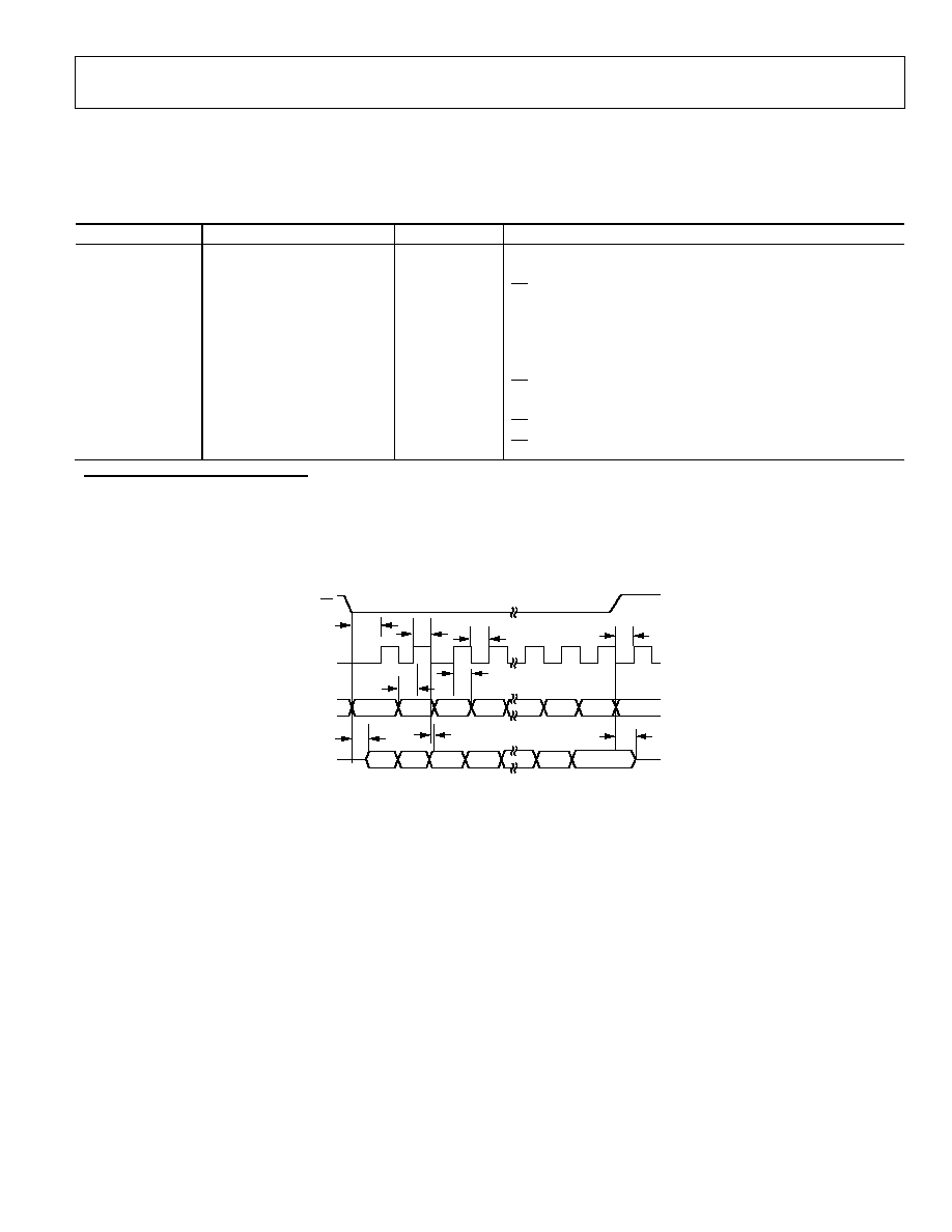
Parameter
Limit at T
MIN
, T
MAX
Unit Description
f
DCLK
1
10
kHz min
20
MHz max
t
1
16
ns min
CS falling edge to first DCLK rising edge
t
2
20
ns min
DCLK high pulse width
t
3
20
ns min
DCLK low pulse width
t
4
12
ns min
DIN setup time
t
5
12
ns min
DIN hold time
t
6
2
16
ns max
CS falling edge to DOUT, three-state disabled
t
7
2
16
ns max
DCLK falling edge to DOUT valid
t
8
3
16
ns max
CS rising edge to DOUT high impedance
t
9
0
ns min
CS rising edge to DCLK ignored
1
Mark/space ratio for the DCLK input is 40/60 to 60/40.
2
Measured with the load circuit of
and defined as the time required for the output to cross 0.4 V or 2.0 V.
Figure 3
Figure 3.
3
t
8
is derived from the measured time taken by the data outputs to change 0.5 V when loaded with the circuit of
The measured number is then extrapolated
back to remove the effects of charging or discharging the 50 pF capacitor. This means that the time, t
8
, quoted in the timing characteristics is the true bus relinquish
time of the part and is independent of the bus loading.
03796-004
DCLK
t
1
t
2
t
3
t
5
t
4
t
6
t
7
t
9
t
8
DIN
MSB
LSB
MSB
LSB
DOUT
1
2
3
15
16
CS
Figure 2. Detailed Timing Diagram
AD7877
Rev. A | Page 6 of 44
ABSOLUTE MAXIMUM RATINGS
T
A
= 25∞C, unless otherwise noted.
Table 3.
Parameter Rating
V
CC
to GND
-0.3 V to +7 V
Analog Input Voltage to GND
-0.3 V to V
CC
+ 0.3 V
Digital Input Voltage to GND
-0.3 V to V
CC
+ 0.3 V
Digital Output Voltage to GND
-0.3 V to V
CC
+ 0.3 V
V
REF
to GND
-0.3 V to V
CC
+ 0.3 V
Input Current to Any Pin Except Supplies
1
10 mA
ESD Rating
2.5 kV
Operating Temperature Range
-40∞C to +85∞C
Storage Temperature Range
-65∞C to +150∞C
Junction Temperature
150∞C
LFCSP Package
Power Dissipation
450 mW
JA
Thermal Impedance
135.7∞C/W
IR Reflow Peak Temperature
220∞C
Pb-Free Parts Only
260∞C (±0.5∞C)
Lead Temperature (Soldering 10 s)
300∞C
1
Transient currents of up to 100 mA do not cause SCR latch-up.
Stresses above those listed under Absolute Maximum Ratings
may cause permanent damage to the device. This is a stress
rating only and functional operation of the device at these or
any other conditions above those listed in the operational
sections of this specification is not implied. Exposure to
absolute maximum rating conditions for extended periods may
affect device reliability.
03796-003
200
µ
A
I
OL
200
µ
A
I
OH
1.6V
TO OUTPUT
PIN
C
L
50pF
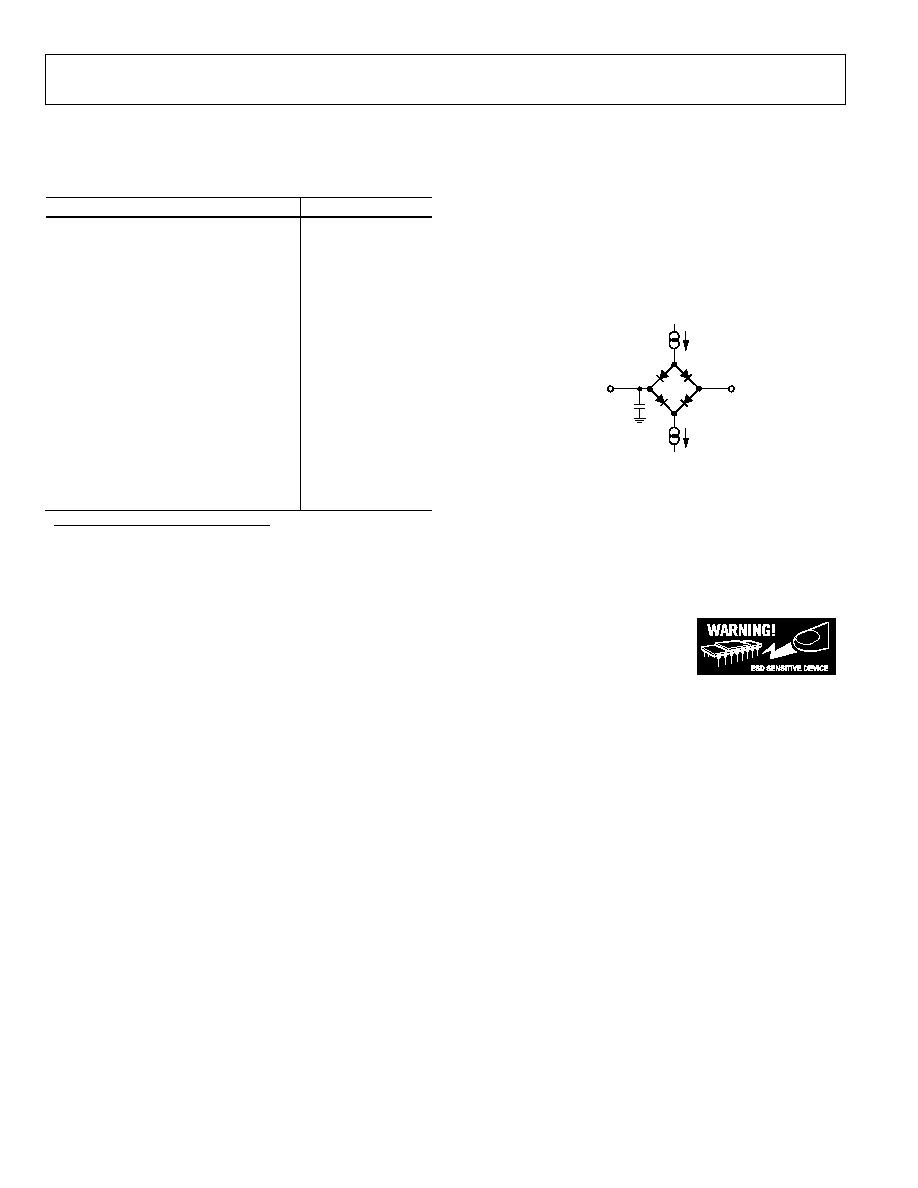
Figure 3. Load Circuit for Digital Output Timing Specifications
ESD CAUTION
ESD (electrostatic discharge) sensitive device. Electrostatic charges as high as 4000 V readily accumulate on
the human body and test equipment and can discharge without detection. Although this product features
proprietary ESD protection circuitry, permanent damage may occur on devices subjected to high energy
electrostatic discharges. Therefore, proper ESD precautions are recommended to avoid performance
degradation or loss of functionality.
AD7877
Rev. A | Page 7 of 44
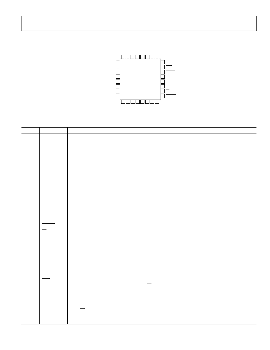
PIN CONFIGURATION AND FUNCTION DESCRIPTIONS
03796-002
NC
1
BAT2
2
BAT1
3
AUX3/GPIO3
4
AUX2/GPIO2
5
AUX1/GPIO1
6
V
CC
7
NC
8
NC
24
DAV
23
ALERT
22
GPIO4
21
STOPACQ
20
DIN
19
CS
18
PENIRQ
17
NC
V
RE
F
AOUT
ARNG
V
DRIV
E
DOUT
DCLK
NC
32 31 30 29 28 27 26 25
NC
X≠
Y≠
X+
Y+
AGND
DGND
NC
9
10 11 12 13 14 15 16
NC = NO CONNECT
AD7877
TOP VIEW
(Not to Scale)
Figure 4. Pin Configuration
Table 4. Pin Function Descriptions
Pin No.
Mnemonic
Description
1
NC
No Connect.
2
BAT2
Battery Monitor Input. ADC Input Channel 7.
3
BAT1
Battery Monitor Input. ADC Input Channel 6.
4
AUX3/GPIO3
Auxiliary Analog Input. ADC Input Channel 5. Can be reconfigured as GPIO pin.
5
AUX2/GPIO2
Auxiliary Analog Input. ADC Input Channel 4. Can be reconfigured as GPIO pin.
6
AUX1/GPIO1
Auxiliary Analog Input. ADC Input Channel 3. Can be reconfigured as GPIO pin.
7
V
CC
Power Supply Input. The V
CC
range for the AD7877 is from 2.2 V to 5.25 V.
8≠9
NC
No Connect.
10
X-
Touch Screen Position Input.
11
Y-
Touch Screen Position Input. ADC Input Channel 2.
12
X+
Touch Screen Position Input. ADC Input Channel 0.
13
Y+
Touch Screen Position Input. ADC Input Channel 1.
14
AGND
Analog Ground. Ground reference point for all analog circuitry on the AD7877. All analog input signals and any
external reference signal should be referred to this voltage.
15
DGND
Digital Ground. Ground reference for all digital circuitry on the AD7877. All digital input signals should be
referred to this voltage.
16, 32
NC
No Connect.
17
PENIRQ
Pen Interrupt. Digital active low output (has 50 k internal pull-up resistor).
18
CS
Chip Select Input. Active low logic input. This input provides the dual function of initiating conversions on the
AD7877 and enabling the serial input/output register.
19
DIN
SPIÆ Serial Data Input. Data to be written to the AD7877's registers should be provided on this input and is
clocked into the register on the rising edge of DCLK.
20
STOPACQ
Stop Acquisition Pin. A signal applied to this pin can be monitored by the AD7877, so that acquisition of new
data by the ADC is halted while the signal is active. Used to reduce the effect of noise from an LCD screen on
the touch screen measurements.
21
GPIO4
Dedicated general-purpose logic input/output pin.
22
ALERT
Digital Active Low Output. Interrupt output, which goes low if a GPIO data bit is set, or if the AUX1, TEMP1,
BAT1, or BAT2 measurements are out of range.
23
DAV
Data Available Output. Active low logic output. Asserts low when new data is available in the AD7877 results
registers. This output is high impedance when CS is high.
24≠25
NC
No Connect.
26
DCLK
External Clock Input. Logic input. DCLK provides the serial clock for accessing data from the part.
27
DOUT
Serial Data Output. Logic output. The conversion result from the AD7877 is provided on this output as a serial
data stream. The bits are clocked out on the falling edge of the DCLK input. This output is high impedance
when CS is high.
28
V
DRIVE
Logic Power Supply Input. The voltage supplied at this pin determines the operating voltage for the serial
interface of the AD7877.

AD7877
Rev. A | Page 8 of 44
Pin No.
Mnemonic
Description
29
ARNG
When the DAC is in current output mode, a resistor from ARNG to GND sets the output range.
30
AOUT
Analog Output Voltage or Current from DAC.
31
V
REF
Reference output for the AD7877. The internal 2.5 V reference is available on this pin for use external to the
device. The reference output must be buffered before it is applied elsewhere in a system. A capacitor of 100nF
is strongly recommended between the V
REF
pin and GND to reduce system noise effects.
Alternatively, an external reference can be applied to this input. The voltage range for the external reference is
1.0 V to V
CC
. For the specified performance, it is 2.5 V on the AD7877.

AD7877
Rev. A | Page 9 of 44
TERMINOLOGY
Integral Nonlinearity
The maximum deviation from a straight line passing through
the endpoints of the ADC transfer function. The endpoints of
the transfer function are zero scale (a point 1 LSB below the
first code transition), and full scale (a point 1 LSB above the last
code transition).
Differential Nonlinearity
The difference between the measured and the ideal 1 LSB
change between any two adjacent codes in the ADC.
Offset Error
The deviation of the first code transition (00...000) to
(00...001) from the ideal (AGND + 1 LSB).
Gain Error
The deviation of the last code transition (111...110) to
(111...111) from the ideal (V
REF
- 1 LSB) after the offset error
has been adjusted out.
On Resistance
A measure of the ohmic resistance between the drain and the
source of the switch drivers.
AD7877
Rev. A | Page 10 of 44
TYPICAL PERFORMANCE CHARACTERISTICS
T
A
= 25∞C, V
CC
= 2.7 V, V
REF
= 2.5 V, f
SAMPLE
= 125 kHz, f
DCLK
= 16 ◊ f
SAMPLE
= 2 MHz, unless otherwise noted.
800
700
600
500
≠50
≠30
≠10
0
30
50
70
90
03796-030
TEMPERATURE (
∞
C)
CURRE
NT (
µ
A)
ADC AND REF
ADC, REF, AND DAC
Figure 5. Supply Current vs. Temperature
1000
400
500
600
700
800
900
2.0
2.3
2.6
2.9
3.2
3.5
3.8
4.1
4.4
4.7
5.0
03796-031
V
CC
(V)
CURRE
NT (
µ
A)
ADC AND REF
ADC, REF, AND DAC
Figure 6. Supply Current vs. V
CC
0.6
≠0.6
≠0.5
≠0.4
≠0.3
≠0.2
≠0.1
0
0.1
0.2
0.3
0.4
0.5
≠50
≠30
≠10
10
30
50
70
90
03796-039
TEMPERATURE (
∞
C)
DELTA FROM 25
∞
C (LS
B
)
Figure 7. Change in ADC Gain vs. Temperature
200
80
100
120
140
160
180
≠50
≠30
≠10
10
30
50
70
90
03796-032
TEMPERATURE (
∞
C)
CURRE
NT (nA)
Figure 8. Full Power-Down I
DD
vs. Temperature
0.6
≠0.6
≠0.5
≠0.4
≠0.3
≠0.2
≠0.1
0
0.1
0.2
0.3
0.4
0.5
≠50
≠30
≠10
10
30
50
70
90
03796-040
TEMPERATURE (
∞
C)
DELTA FROM 25
∞
C (LS
B
)
Figure 9. Change in ADC Offset vs. Temperature
1.0
≠1.0
≠0.8
≠0.6
≠0.4
≠0.2
0
0.2
0.4
0.6
0.8
0
500
1000
1500
2000
2500
3000
3500
4000
03796-044
CODE
INL (LSB)
Figure 10. ACD INL Plot
AD7877
Rev. A | Page 11 of 44
1.0
≠1.0
≠0.8
≠0.6
≠0.4
≠0.2
0
0.2
0.4
0.6
0.8
0
500
1000
1500
2000
2500
3000
3500
4000
03796-045
CODE
DNL (LS
B
)
Figure 11. ADC DNL Plot
22
8
10
12
14
16
18
20
2.7
3.1
3.5
3.9
4.3
4.7
5.1
5.5
03796-048
V
DD
(V)
R
ON
(
)
Y+ TO V
DD
Y≠ TO GND
X+ TO V
DD
X≠ TO GND
Figure 12. Switch On Resistance vs. V
CC
(X+, Y+: V
CC
to Pin; X-, Y-: Pin to GND)
22
8
10
12
14
16
18
20
≠40
≠20
0
20
40
60
80
03796-049
TEMPERATURE (
∞
C)
R
ON
(
)
Y+ TO V
DD
Y≠ TO GND
X+ TO V
DD
X≠ TO GND
Figure 13. Switch On Resistance vs. Temperature
(X+, Y+: V
CC
to Pin; X-, Y-: Pin to GND)
16
14
12
10
8
6
4
2
0
≠50
90
70
50
30
10
≠10
≠30
03796-046
TEMPERATURE (
∞
C)
RE
FE
RE
NCE
CURRE
NT (
µ
A)
Figure 14. External Reference Current vs. Temperature
2.520
2.515
2.510
2.505
2.500
2.495
2.490
2.485
2.480
2.475
≠50
≠30
≠10
10
30
50
70
90
03796-033
TEMPERATURE (
∞
C)
V
RE
F
(V
)
Figure 15. Internal V
REF
vs. Temperature
2.508
2.496
2.498
2.500
2.502
2.504
2.506
2.6
2.9
3.2
3.5
3.8
4.1
4.4
4.7
5.0
03796-034
V
CC
(V)
V
RE
F
(V
)
Figure 16. Internal V
REF
vs. V
CC
AD7877
Rev. A | Page 12 of 44
3145
3135
3125
3115
3105
3095
3085
3075
3065
3055
3045
≠50
≠30
≠10
10
30
50
70
90
03796-041
TEMPERATURE (
∞
C)
ADC CODE
(De
c
i
ma
l)
Figure 17. ADC Code vs. Temperature (2.7 V Supply)
1183
1176
1177
1178
1179
1180
1181
1182
2.7
2.8
2.9
3.0
3.1
3.2
3.3
3.4
3.5
3.6
03796-042
V
CC
(V)
TE
MP
1
CODE
Figure 18. Temp1 vs. V
CC
982
975
976
977
978
979
980
981
2.7
2.8
2.9
3.0
3.1
3.2
3.3
3.4
3.5
3.6
03796-043
V
CC
(V)
TE
MP
0
CODE
Figure 19. Temp0 vs. V
CC
03796-047
INTE
RNAL V
REF
(V
)
TURN-ON TIME (
µ
s)
0
3
6
20
40
60
80
100
120
≠20
0
NO CAP
0.711
µ
s SETTLING TIME
100nF CAP
54.64
µ
s SETTLING TIME
Figure 20. Internal V
REF
vs. Turn-On Time
10
≠150
≠130
≠110
≠90
≠70
≠50
≠30
≠10
0
10k
20k
30k
SNR 70.25dB
THD 78.11dB
40k
03796-035
FREQUENCY
INP
U
T TONE
AMPLITUDE
(dB)
Figure 21. Typical FFT Plot for the Auxiliary Channels of the AD7877
at 90 kHz Sample Rate and 10 kHz Input Frequency
3.50
0
0.25
0.50
0.75
1.00
1.25
1.50
1.75
2.00
2.25
2.50
2.75
3.00
3.25
0
1
2
3
4
5
6
7
8
9
10
03796-036
SOURCE/SINK CURRENT (mA)
DAC O/P LEVEL (V)
DAC O/P SOURCE ABILITY
DAC O/P SINK ABILITY
Figure 22. DAC Source and Sink Current Capability
AD7877
Rev. A | Page 13 of 44
03796-037
CH1
200mV CH2 100mV
M2.00
µ
s
CH1 780mV
1
: 144mV
@: 1.296V
V
DD
= 3V
TEMPERATURE = 25
∞
C
Figure 23. DAC O/P Settling Time (Zero Scale to Half-Scale)
600
500
400
300
200
100
0
0
25
50
75
100
125
150
175
200
225
250
03796-038
INPUT CODE (Decimal)
DAC S
I
NK CURRE
NT (
µ
A)
DAC SINK CURRENT
Figure 24. DAC Sink Current vs. Input Code
≠2
≠1
0
1
2
03796-050
ERROR (%)
Figure 25. Typical Accuracy for Battery Channel (25∞C)
AD7877
Rev. A | Page 14 of 44
CIRCUIT INFORMATION
The AD7877 is a complete, 12-bit data acquisition system for
digitizing positional inputs from a touch screen in PDAs and
other devices. In addition, it can monitor two battery voltages,
ambient temperature, and three auxiliary analog voltages, with
high and low limit comparisons on three of the inputs, and has
up to four general-purpose logic I/O pins.
The core of the AD7877 is a high speed, low power, 12-bit
analog-to-digital converter (ADC) with input multiplexer,
on-chip track-and-hold, and on-chip clock. The results of
conversions are stored in 11 results registers, and the results
from one auxiliary input and two battery inputs can be
compared with high and low limits stored in limit registers to
generate an out-of-limit ALERT. The AD7877 also contains low
resistance analog switches to switch the X and Y excitation
voltages to the touch screen, a STOPACQ pin to control the
ADC acquisition period, 2.5 V reference, on-chip temperature
sensor, and 8-bit DAC to control LCD contrast. The high speed
SPI serial bus provides control of, and communication with, the
device.
Operating from a single supply from 2.2 V to 5 V, the AD7877
offers throughput rates of up to 125 kHz. The device is available
in a 5 mm by 5 mm 32-lead lead frame chip scale package.
The data acquisition system of the AD7877 has a number of
advanced features:
∑
Input channel sequenced automatically or selected by
the host
∑
STOPACQ feature to reduce noise from LCD
∑
Averaging of from 1 to 16 conversions for noise
reduction
∑
Programmable acquisition time
∑
Power management
∑
Programmable ADC power-up delay before first
conversion
∑
Choice of internal or external reference
∑
Conversion at preprogrammed intervals
TOUCH SCREEN PRINCIPLES
A 4-wire touch screen consists of two flexible, transparent,
resistive-coated layers that are normally separated by a small air
gap. The X layer has conductive electrodes running down the
left and right edges, allowing the application of an excitation
voltage across the X layer from left to right.
03796-005
X+
X≠
Y≠
Y+
CONDUCTIVE ELECTRODE
ON BOTTOM SIDE
PLASTIC FILM WITH
TRANSPARENT, RESISTIVE
COATING ON BOTTOM SIDE
PLASTIC FILM WITH
TRANSPARENT, RESISTIVE
COATING ON TOP SIDE
LCD SCREEN
CONDUCTIVE ELECTRODE
ON TOP SIDE
Figure 26. Basic Construction of a Touch Screen
The Y layer has conductive electrodes running along the top
and bottom edges, allowing the application of an excitation
voltage down the layer from top to bottom.
Provided that the layers are of uniform resistivity, the voltage at
any point between the two electrodes is proportional to the
horizontal position for the X layer and the vertical position for
the Y layer.
When the screen is touched, the two layers make contact. If only
the X layer is excited, the voltage at the point of contact, and
therefore the horizontal position, can be sensed at one of the
Y layer electrodes. Similarly, if only the Y layer is excited, the
voltage, and therefore the vertical position, can be sensed at one
of the X electrodes. By switching alternately between X and
Y excitation and measuring the voltages, the X and Y coordi-
nates of the contact point can be found.
In addition to measuring the X and Y coordinates, it is also
possible to estimate the touch pressure by measuring the
contact resistance between the X and Y layers. The AD7877 is
designed to facilitate this measurement.
Figure 28 shows an equivalent circuit of the analog input
structure of the AD7877, showing the touch screen switches, the
main analog multiplexer, the ADC with analog and differential
reference inputs, and the dual 3-to-1 multiplexer that selects the
reference source for the ADC.
AD7877
Rev. A | Page 15 of 44
AUX3/GPIO4
BAT1
BAT2
AUX2/GPIO3
AUX1/GPIO2
12-BIT SUCCESSIVE
APPROXIMATION ADC
WITH TRACK-AND-HOLD
9 TO 1
I/P
MUX
TEMPERATURE
SENSOR
Y≠
Y+
X≠
X+
V
CC
REF≠
IN+
REF
INT/EXT
REF+
DUAL 3-1
MUX
X≠ Y≠ GND X+ Y+ V
REF
03796-006
Figure 27. Analog Input Structure
The AD7877 can be set up to convert specific input channels or
to convert a sequence of channels automatically. The results of
the ADC conversions are stored in the results registers. See the
Serial Interface section for details.
When measuring the ancillary analog inputs (AUX1 to AUX3,
BAT1 and BAT2), the ADC uses the internal reference, or an
external reference applied to the V
REF
pin, and the measurement
is referred to GND.
MEASURING TOUCH SCREEN INPUTS
When measuring the touch screen inputs, it is possible to
measure using the internal (or external) reference, or to use the
touch screen excitation voltage as the reference and perform a
ratiometric, differential measurement. The differential method
is the default and is selected by clearing the SER/DFR bit
(Bit 11) in Control Register 1. The single-ended method is
selected by setting this bit.
Single-Ended Method
The single-ended method is illustrated for the Y position in
Figure 28. For the X position, the excitation voltage would be
applied to X+ and X- and the voltage measured at Y+.
03796-007
ADC
REF+
INPUT
(VIA MUX)
X+
REF≠
TOUCH
SCREEN
Y+
Y≠
GND
V
REF
V
CC
Figure 28. Single-Ended Conversion of Touch Screen Inputs
The voltage seen at the input to the ADC in Figure 28 is
V
IN
= V
CC
◊
YTOTAL
Y
R
R
-
(1)
The advantage of the single-ended method is that the touch
screen excitation voltage can be switched off once the signal has
been acquired. Because a screen can draw over 1 mA, this is a
significant consideration for a battery-powered system.
The disadvantages of the single-ended method are as follows:
∑
It can be used only if V
CC
is close to V
REF
. If V
CC
is greater than
V
REF
, some positions on the screen are outside the range of
the ADC. If V
CC
is less than V
REF
, the full range of the ADC is
not utilized.
∑
The ratio of V
CC
to V
REF
must be known. If V
REF
and/or V
CC
vary relative to one another, this can introduce errors.
∑
Voltage drops across the switches can introduce errors. Touch
screens can have a total end-to-end resistance of from 200
to 900 . Taking the lowest screen resistance of 200 and a
typical switch resistance of 14 , this could reduce the appar-
ent excitation voltage to 200/228 ◊ 100 = 87% of its actual
value. In addition, the voltage drop across the low-side switch
adds to the ADC input voltage. This introduces an offset into
the input voltage, which means that it can never reach zero.
The single-ended method is adequate for applications in which
the input device is a fairly blunt and imprecise instrument such
as a finger.
Ratiometric Method
The ratiometric method is illustrated in Figure 29. Here, the
negative input of the ADC reference is tied to Y- and the
positive input is connected to Y+, so the screen excitation
voltage provides the reference for the ADC. The input of the
ADC is connected to X+ to determine the Y position.
03796-008
ADC
REF+
INPUT
(VIA MUX)
REF≠
V
CC
X+
TOUCH
SCREEN
Y+
Y≠
GND
Figure 29. Ratiometric Conversion of Touch Screen Inputs

AD7877
Rev. A | Page 16 of 44
For greater accuracy, the ratiometric method has two significant
advantages:
∑
The reference to the ADC is provided from the actual voltage
across the screen, so voltage drops across the switches have
no effect.
∑
Because the measurement is ratiometric, it does not matter if
the voltage across the screen varies in the long term. However,
it must not change after the signal has been acquired.
The disadvantage of the ratiometric method is that the screen
must be powered up all the time, because it provides the
reference voltage for the ADC.
TOUCH-PRESSURE MEASUREMENT
The pressure applied to the touch screen via a pen or finger can
also be measured with the AD7877 using some simple calcula-
tions. The contact resistance between the X and Y plates is
measured. This provides a good indication of the size of the
depressed area and, therefore, the applied pressure. The area of
the spot touched is proportional to the size of the object
touching it. The size of this resistance (R
TOUCH
) can be calculated
using two different methods.
First Method
The first method requires the user to know the total resistance
of the X-plate tablet (R
X
). Three touch screen conversions are
required:
∑
Measurement of the X position, X
POSITION
(Y+ input).
∑
Measurement of the Y- input with the excitation voltage
applied to Y+ and X- (Z1 measurement).
∑
Measurement of the X+ input with the excitation voltage
applied to Y+ and X- (Z2 measurement).
These three measurements are illustrated in Figure 30.
The AD7877 has two special ADC channel settings that
configure the X and Y switches for Z1 and Z2 measurement and
store the results in the Z1 and Z2 results registers. The Z1
measurement is ADC Channel 1010b, and the result is stored in
the register with Read Address 11010b. The Z2 measurement is
ADC Channel 0010b, and the result is stored in the register with
Read Address 10010b.
The touch resistance can then be calculated using the following
equation:
R
TOUCH
= (
R
XPlate
) ◊ (
X
POSITION
/4096 ◊ [
Z2/Z1) - 1]
(2)
03796-009
Y≠
Y+
X≠
X+
TOUCH
RESISTANCE
MEASURE
Z1 POSITION
X≠
X+
Y≠
Y+
TOUCH
RESISTANCE
MEASURE
X POSITION
Y≠
Y+
X≠
X+
TOUCH
RESISTANCE
MEASURE
Z2 POSITION
Figure 30. Three Measurements Required for Touch Pressure
Second Method
The second method requires that the resistance of the X-plate
and Y-plate tablets be known. Three touch screen conversions
again are required, a measurement of the X Position (X
POSITION
),
Y Position (Y
POSITION
), and Z1 position.
The following equation also calculates the touch resistance:
R
TOUCH
=
R
XPlate
◊ (
X
POSITION
/4096) ◊ [(4096/
Z1) - 1]
-
R
YPlate
◊ [1 - (
Y
POSITION
/4096)]
(3)
STOPACQ PIN
As explained previously, touch screens are composed of two
resistive layers, normally placed over an LCD screen. Because
these layers are in close proximity to the LCD screen, noise can
be coupled from the screen onto these resistive layers, causing
errors in the touch screen positional measurements.
For example, a jitter might be noticeable in the cursor on-
screen. In most LCD touch screen systems, a signal, such as an
LCD invert signal or other control signal, is present, and noise is
usually coupled onto the touch screen during this signal's active
period, as shown in Figure 31.
03796-010
LCD SIGNAL
TOUCH SCREEN
SIGNAL
NOISY
PERIOD
NOISY
PERIOD
Figure 31. LCD Noise Affects Touch Screen Measurements

AD7877
Rev. A | Page 17 of 44
It is only during the sample or acquisition phase of the
AD7877's ADC operation that noise from the LCD screen has
an effect on the ADC's measurements. During the hold or
conversion phase, the noise has no effect, because the voltage at
the input of the ADC has already been acquired. Therefore, to
minimize the effect of noise on the touch screen measurements,
the ADC acquisition phase should be halted.
The LCD control signal should be applied to the STOPACQ pin.
To ensure that acquisition never takes place during the noisy
period when the LCD signal is active, the AD7877 monitors this
signal. No acquisitions take place when the control signal is
active. Any acquisition that is in progress when the signal
becomes active is aborted and restarts when the signal becomes
inactive again.
To accommodate signals of different polarities on the
STOPACQ pin, a user-programmable register bit is used to
indicate whether the signal is active high or low. The POL bit is
Bit 3 in Control Register 2, Address 02h. Setting POL to 1
indicates that the signal on STOPACQ is active high; setting
POL to 0 indicates that it is active low. POL defaults to 0 on
power-up. To disable monitoring of STOPACQ, the pin should
be tied low if POL = 1, or tied high if POL = 0. Under no
circumstances should the pin be left floating.
The signal on STOPACQ has no effect while the ADC is in
conversion mode, or during the first conversion delay time. (See
the Control Registers section for details on first conversion
delay.)
When enabled, the STOPACQ monitoring function is imple-
mented on all input channels to the ADC: AUX1, AUX2, BAT1,
BAT2, TEMP1, and TEMP2, as well as on the touch screen input
channels.
TEMPERATURE MEASUREMENT
Two temperature measurement options are available on the
AD7877: the single conversion method and the differential
conversion method. The single conversion method requires
only a single measurement on ADC Channel 1000b. Differential
conversion requires two measurements, one on ADC Channel
1000b and a second on ADC Channel 1001b. The results are
stored in the results registers with Addresses 11000b (TEMP1)
and 11001b (TEMP2). The AD7877 does not provide an explicit
output of the temperature reading. Some external calculations
must be performed by the system. Both methods are based on
an on-chip diode measurement.
Single Conversion Method
The single conversion method makes use of the fact that the
temperature coefficient of a silicon diode is approximately
-2.1 mV/∞C. However, this small change is superimposed on the
diode forward voltage, which can have a wide tolerance. It is,
therefore, necessary to calibrate by measuring the diode voltage
at a known temperature to provide a baseline from which the
change in forward voltage with temperature can be measured.
This method provides a resolution of approximately 0.3∞C and a
predicted accuracy of ±2.5∞C.
The temperature limit comparison is performed on the result in
the TEMP1 results register, which is simply the measurement of
the diode forward voltage. The values programmed into the
high and low limits should be referenced to the calibrated diode
forward voltage to make accurate limit comparisons. An
example is shown in the Limit Comparison section.
Differential Conversion Method
The differential conversion method is a 2-point measurement.
The first measurement is performed with a fixed bias current
into a diode (when the TEMP1 channel is selected), and the
second measurement is performed with a fixed multiple of the
bias current into the same diode (when the TEMP2 channel is
selected). The voltage difference in the diode readings is
proportional to absolute temperature and is given by the
following formula:
V
BE
= (
KT/q) ◊ (1n N)
(4)
where:
V
BE
represents the diode voltage.
N is the bias current multiple (typical value for AD7877 =120).
k is Boltzmann's constant.
q is the electron charge.
This method provides a resolution of approximately 1.6∞C, and
a guaranteed accuracy of ±4∞C without calibration. Determina-
tion of the N value on a part-by-part basis improves accuracy.
Assuming a current multiple of 120, which is a typical value for
the AD7877, taking Boltzmann's constant,
k = 1.38054 ◊
10
-23
electrons V/∞K, the electron charge
q = 1.602189 ◊ 10
-19
,
then
T, the ambient temperature in Kelvin, would be calculated
as follows:
V
BE
= (
KT/q) ◊ (1n N)
T∞K = (V
BE
◊ q)/(k ◊ 1n N)
= V
BE
◊ 1.602189 ◊ 10
-19
)/(1.38054 ◊ 10
-23
◊ 4.65)
T∞C = 2.49 ◊ 103 ◊ V
BE
- 273
V
BE
is calculated from the difference in readings from the first
conversion and second conversion. The user must perform the
calculations to get
V
BE
, and then calculate the temperature
value in degrees.
Figure 32 shows a block diagram of the temperature
measurement circuit.
AD7877
Rev. A | Page 18 of 44
03796-011
TEMP1
TEMP2
MUX
ADC
I
V
BE
105
◊
I
Figure 32. Block Diagram of Temperature Measurement Circuit
Temperature Calculations
If an explicit temperature reading in ∞C is required, then this
can be calculated as follows for the single measurement
method:
1.
Calculate the scale factor of the ADC in degrees per LSB:
Degrees per LSB = ADC LSB size/-2.1 mV =
V
REF
/4096)/
-2.1 mV
2.
Save the ADC output
D
CAL
at the calibration temperature
T
CAL
.
3.
Take ADC reading
D
AMB
at temperature to be measured
T
AMB
.
4.
Calculate the difference in degrees between
T
CAL
and
T
AMB
using
T = (D
AMB
- D
CAL
) ◊
degrees per LSB
5.
Add
T to T
CAL
.
Example:
The internal 2.5 V reference is used.
1.
Degrees per LSB = (2.5/4096)/-2.1 ◊ 10
-3
=
-0.291.
2.
The ADC output is 983 decimal at 25∞C, equivalent to a
diode forward voltage of 0.6 V.
3.
The ADC output at
T
AMB
is 880.
4.
T = (880 - 983) ◊ -0.291 = 30∞.
5.
T
AMB
= 25 + 30 = 55∞C.
To calculate the temperature explicitly using the differential
method:
1.
Calculate the LSB size of the ADC in V:
LSB = V
REF
/4096
2.
Subtract
TEMP1 from TEMP2 and multiply by LSB size to
get
V
BE
.
3.
Multiply by 2490 and subtract 273 to get the temperature
in ∞C.
Example:
The internal 2.5 V reference is used.
1.
LSB size = 2.5 V/4096 = 6.1 ◊ 10
-4
V (610 µV).
2.
TEMP1 = 880 and TEMP2 = 1103:
V
BE
= (1103
- 880) ◊ 6.1◊ 10
-4
= 0.136 V
3.
T = 0.136 ◊ 2490 - 273 = 65∞C.
BATTERY MEASUREMENT
The AD7877 can monitor battery voltages from 0.5 V to 5 V on
two inputs, BAT1 and BAT2. Figure 33 shows a block diagram
of a battery voltage monitored through the BAT1 pin. The
voltage to the V
CC
pin of the AD7877 is maintained at the
desired supply voltage via the dc/dc regulator while the input to
the regulator is monitored. This voltage on BAT1 is divided
down by 2 internally, so that a 5 V battery voltage is presented to
the ADC as 2.5 V. To conserve power, the divider circuit is on
only during the sampling of a voltage on BAT1. The BAT2 input
circuitry is identical.
The BAT1 input is ADC Channel 0110b and the result is stored
in Register 10110b. The BAT2 input is ADC Channel 0111b and
the result is stored in Register 10111b.
03796-012
ADC
0.25V≠2.5V
SW
BAT1
V
CC
V
REF
5k
5k
DC-DC
CONVERTER
BATTERY
0.5V TO 5V
Figure 33. Block Diagram of Battery Measurement Circuit
Figure 33 shows the ADC using the internal reference of 2.5 V.
If a different reference voltage is used, then the maximum
battery voltage that the AD7877 can measure changes. The
maximum voltage measurable is V
REF
◊ 2, because this voltage
gives a full-scale output from the ADC. If a smaller reference is
used, such as 2 V, then the maximum battery voltage measurable
is 4 V. If a larger reference is used, such as 3.5 V, then the
maximum battery voltage measurable is 7 V. The internal
reference is particularly suited for use when measuring Li-Ion
batteries, where the minimum voltage is about 2.7 V and the
maximum is about 4.2 V. A proper choice of external reference
ensures that other voltage ranges can be accommodated.

AD7877
Rev. A | Page 19 of 44
AUXILIARY INPUTS
The AD7877 has three auxiliary analog inputs, AUX1 to AUX3.
These channels have a full-scale input range from 0 V to V
REF
.
The ADC channel addresses for AUX1 to AUX3 are 0011b,
0100b, and 0101b, and the results are stored in Registers 10011b,
10100b, and 10101b. These pins can also be reconfigured as
general-purpose logic inputs/outputs, as described in the GPIO
Configuration section.
LIMIT COMPARISON
The AUX1 measurement, the two battery measurements, and
the TEMP1 measurement can all be compared with high and
low limits, and an out-of-limit result made to generate an alarm
output at the ALERT pin. The limits are stored in registers with
addresses from 00100b to 01011b. After a measurement from
any one of the four channels is converted, it is compared with
the corresponding high and low limits. An out-of-limit result
sets one of the status bits in the alert status/enable register. For
details on these and other registers, see the Register Maps and
Detailed Register Descriptions sections. For details on writing
and reading data, see the Serial Interface section.
As mentioned previously, the temperature comparison is made
using the result of the TEMP1 measurement, which is the diode
forward voltage. Because the temperature coefficient of the
diode is known but the actual forward voltage can have a wide
tolerance, it is not possible to program the high and low limit
registers with predetermined values.
Instead, it is necessary to calibrate the temperature measure-
ment, calculate the TEMP1 readings at the high and low limit
temperatures, and then program those values into the limit
registers, as follows:
1.
Calculate
LSB per degree = -2.1 mV/(V
REF
/4096).
2.
Save the calibration reading
D
CAL
at calibration temperature
T
CAL
.
3.
Subtract
T
CAL
from limit temperatures
T
HIGH
and
T
LOW
to get
the difference in degrees between the limit temperatures
and the calibration temperature.
4.
Multiply this value by
LSB per degree to get the value in
LSBs.
5.
Add these values to the digital value at the calibration
temperature to get the digital high and low limit values.
Example:
The internal 2.5 V reference is used.
1.
T
HIGH
= +65∞C and
T
LOW
=
-10∞C.
2.
LSB per degree = -2.1 ◊ 10
-3
/(2.5/4096) =
-3.44.
3.
D
CAL
= 983 decimal at 25∞C.
4.
D
HIGH
= (65
- 25) ◊ -3.44 + 983 = 845.
5.
D
LOW
= (
-10 - 25) ◊ -3.44 + 983 = 1103.
AD7877
Rev. A | Page 20 of 44
CONTROL REGISTERS
Control Register 1 contains the ADC channel address, the
SER/DFR bit (to choose single or differential methods of touch
screen measurement), the register read address, and the ADC
mode bits. Control Register 1 should always be the last register
to be programmed prior to starting conversions. Its power-on
default value is 00h. To change any parameter after conversion
has begun, the part should first be put into mode 00, the
changes made, and then Control Register 1 reprogrammed,
ensuring that it is always the last register to be programmed
before conversions begin.
03796-013
SER/
DFR
CHNL
ADD
3
CHNL
ADD
2
CHNL
ADD
1
CHNL
ADD
0
RD
ADD
4
RD
ADD
3
RD
ADD
2
RD
ADD
1
RD
ADD
0
ADC
MODE
1
ADC
MODE
0
11
0
Figure 34. Control Register 1
Control Register 2 sets the timer, reference, polarity, first
conversion delay, averaging, and acquisition time. Its power-on
default value is 00h. See the Detailed Register Descriptions
section for more information on the control registers.
03796-014
AVG
1
AVG
0
ACQ
1
ACQ
0
PM
1
PM
0
FCD
1
FCD
0
POL
REF
TMR
1
TMR
0
11
0
Figure 35. Control Register 2
CONTROL REGISTER 1
ADC Mode (Control Register 1 Bits <1:0>)
These bits select the operating mode of the ADC. The AD7877
has three operating modes. These are selected by writing to the
mode bits in Control Register 1. If the mode bits are 00, no
conversion is performed.
Table 5. Control Register 1 Mode Selection
Mode 1
Mode 0
Function
0
0
Do not convert (default)
0
1
Single-channel conversion, AD7877 in
slave mode
1
0
Sequence 0, AD7877 in slave mode
1
1
Sequence 1, AD7877 in master mode
If the mode bits are 01, a single conversion is performed on the
channel selected by writing to the channel bits of Control
Register 1 (Bits 7 to 10). At the end of the conversion, if the
TMR bits in Control Register 2 are set to 00, the mode bits
revert to 00 and the ADC returns to no convert mode until a
new conversion is initiated by the host. Setting the TMR bits to
a value other than 00 causes the conversion to be repeated, as
described in the Timer (Control Register 2 Bits <1:0>) section.
The flowchart in Figure 37 shows how the AD7877 operates in
mode 01.
The AD7877 can also be programmed to convert a sequence of
selected channels automatically. The two modes for this type of
conversion are slave mode and master mode.
For slave mode operation, the channels to be digitized are
selected by setting the corresponding bits in Sequencer
Register 0. Conversion is initiated by writing 10b to the mode
bits of Control Register 1. The ADC then digitizes the selected
channels and stores the results in the corresponding results
registers. At the end of the conversion, if the TMR bits in
Control Register 2 are set to 00, the mode bits revert to 00 and
the ADC returns to no convert mode until a new conversion is
initiated by the host. Setting the TMR bits to a code other than
00 causes the conversion sequence to be repeated. The flowchart
in Figure 38 shows how the AD7877 operates in mode 10.
For master mode operation, the channels to be digitized are
written to Sequencer Register 1. Master mode is then selected
by writing 11 to the mode bits in Control Register 1. In this
mode, the wake-up on touch feature is active, so conversion
does not begin immediately. The AD7877 waits until the screen
is touched before beginning the sequence of conversions. The
ADC then digitizes the selected channels, and the results are
written to the results registers. The AD7877 waits for the screen
to be touched again, or for a timer event if the screen remains
touched, before beginning another sequence of conversions.
Figure 39 is a flowchart, showing how the AD7877 operates in
mode 11.
ADC Channel (Control Register 1 Bits <10:7>)
The ADC channel is selected by Bits 10:7 of Control Register 1
(CHADD3 to CHADD0). In addition, the SER/DFR bit, Bit 11,
selects between single-ended and differential conversion. A
complete list of channel addresses is given in Table 6.
For mode 0 (single-channel) conversion, the channel is selected
by writing the appropriate CHADD3 to CHADD0 code to
Control Register 1.
For sequential channel conversion, channels to be converted are
selected by setting bits corresponding to the channel number in
Sequencer Register 1 for slave mode sequencing or Sequencer
Register 2 for master mode sequencing.
For both single-channel and sequential conversion, normal
(single-ended) conversion is selected by clearing the SER/DFR
bit in Control Register 1. Ratiometric (differential) conversion is
selected by setting the SER/DFR bit.

AD7877
Rev. A | Page 21 of 44
Table 6. Codes for Selecting Input Channel and Normal or Ratiometric Conversion
Channel
SER/DFR
CHADD(3:0)
Analog Input
X Switches
Y Switches
+REF
-REF
0
0
0 0 0 0
X+ (Y Position)
OFF
ON
Y+
Y-
1
0
0 0 0 1
Y+ (X Position)
ON
OFF
X+
X-
2
0
0 0 1 0
Y- (Z2)
X+ OFF, X- ON
Y+ ON, Y- OFF
Y+
X-
3
0
0 01 1
AUX1
OFF
OFF
V
REF
GND
4
0
0 1 00
AUX2
OFF
OFF
V
REF
GND
5
0
0 1 0 1
AUX3
OFF
OFF
V
REF
GND
6
0
0 1 1 0
BAT1
OFF
OFF
V
REF
GND
7
0
0 1 1 1
BAT2
OFF
OFF
V
REF
GND
8
0
1 0 0 0
TEMP1
OFF
OFF
V
REF
GND
9
0
1 0 0 1
TEMP2
OFF
OFF
V
REF
GND
10
0
1 0 1 0
X+ (Z1)
X+ OFF, X- ON
Y+ ON, Y- OFF
Y+
X-
-
0
1 0 1 1
INVALID ADDRESS
-
0
1 1 0 0
INVALID ADDRESS
-
0
1 1 0 1
INVALID ADDRESS
-
0
1 1 1 0
INVALID ADDRESS
-
0
1 1 1 1
INVALID ADDRESS
0
1
0 0 0 0
X+ (Y Position)
OFF
ON
V
REF
GND
1
1
0 0 0 1
Y+ (X Position)
ON
OFF
V
REF
GND
2
1
0 0 1 0
Y- (Z2)
X+ OFF, X- ON
Y+ ON, Y- OFF
V
REF
GND
3
1
0 0 1 1
AUX1
OFF
OFF
V
REF
GND
4
1
0 1 0 0
AUX2
OFF
OFF
V
REF
GND
5
1
0 1 0 1
AUX3
OFF
OFF
V
REF
GND
6
1
0 1 1 0
BAT1
OFF
OFF
V
REF
GND
7
1
0 1 1 1
BAT2
OFF
OFF
V
REF
GND
8
1
1 0 0 0
TEMP1
OFF
OFF
V
REF
GND
9
1
1 0 0 1
TEMP2
OFF
OFF
V
REF
GND
10
1
1 0 1 0
X+ (Z1)
X+ OFF, X- ON
Y+ ON, Y- OFF
V
REF
GND
-
1
10 1 1
INVALID ADDRESS
-
1
1 1 0 0
INVALID ADDRESS
-
1
1 1 0 1
INVALID ADDRESS
-
1
1 1 1 0
INVALID ADDRESS
-
1
1 1 1 1
INVALID ADDRESS
CONTROL REGISTER 2
Timer (Control Register 2 Bits <1:0>)
The TMR bits in Control Register 2 enable the ADC to
repeatedly perform a conversion or conversion sequence either
once only or at intervals of 512 µs, 1.024 ms, or 8.19 ms. In slave
mode, the timer starts as soon as the conversion sequence is
finished. In master mode, the timer starts at the end of a conver-
sion sequence only if the screen remains touched. If the touch is
released at any stage, then the timer stops and, the next time the
screen is touched, a conversion sequence begins immediately.
Table 7. Control Register 2 Timer Selection
TMR1
TMR0
Function
0
0
Convert only once (default)
0
1
Every 1024 clocks (512 µs)
1
0
Every 2048 clocks (1.024 ms)
1
1
Every 16,384 clocks (8.19 ms)
Int/Ext Reference (Control Register 2 Bit <2>)
If the REF bit in Control Register 2 is 0 (default value), the
internal reference is selected. If any connection is made to V
REF
while the internal reference is selected (for example, to supply a
reference to other circuits), it should be buffered. An external
power supply should not be connected to this pin while REF is
equal to 0, because it might overdrive the internal reference.
Note also that, because the internal reference is 2.5 V, it operates
only with supply voltages down to 2.7 V. Below this value an
external reference should be used.
If the REF bit is 1, the V
REF
pin becomes an input and the
internal reference is powered down. This overrides any setting
of the PM bits with regard to the reference. An external
reference can then be applied to the REF pin.
AD7877
Rev. A | Page 22 of 44
STOPACQ Polarity (Control Register 2 Bit <3>)
This bit should be set according to the polarity of the signal
applied to the STOPACQ pin. If that signal is active high, that is,
no acquisitions should occur during the signal's high period,
then the POL bit should be set to 1. If the signal is active low,
then the POL bit should be 0. The default value for POL is 0.
First Conversion Delay (Control Register 2 Bits <5:4> )
The first conversion delay (FCD) bits in Control Register 2
program a delay of 500 ns (default), 128 µs, 1.024 ms, or 8.19 ms
before the first conversion, to allow the ADC time to power up.
This delay also occurs before conversion of the X and Y
coordinate channels, to allow extra time for screen settling, and
after the last conversion in a sequence, to precharge PENIRQ. If
the signal on the STOPACQ pin is being monitored and goes
active during the FCD, it is ignored until after the FCD period.
Table 8. First Conversion Delay Selection
FCD1 FCD Function
0
0
1 clock delay (500 ns)
0
1
256 clocks delay (128 µs)
1
0
2048 clocks delay (1.024 ms)
1
1
16,384 clocks delay (8.19 ms)
Power Management (Control Register 2 Bits <7:6>)
The power management (PM) bits in Control Register 2 allow
the power management features of the ADC to be programmed.
If the PM bits are 00, the ADC is powered down permanently.
This overrides any setting of the mode bits in Control
Register 1. If the PM bits are 01, the ADC and the reference
both power down when the ADC is not converting. If the PM
bits are 10, the ADC and reference are powered up continuously.
If the PM bits are 11, the ADC, but not the reference, powers
down when the ADC is not converting.
Table 9. Power Management Selection
PM1
PM0
Function
0
0
Power down continuously (default)
0
1
Power down ADC and reference when
ADC is not converting (powers up with
FCD at start of conversion)
1
0
Powered up continuously
1
1
Power down ADC when ADC is not
converting (powers up with FCD at start
of conversion)
Acquisition Time (Control Register 2 Bits <9:8>)
The ACQ bits in Control Register 2 allow the selection of
acquisition times for the ADC of 2 µs (default), 4 µs, 8 µs, or
16 µs. The user can program the ADC with an acquisition time
suitable for the type of signal being sampled. For example,
signals with large RC time constants might require longer
acquisition times.
Table 10. Acquisition Time Selection
ACQ1
ACQ0
Function
0
0
4 clock periods (2 µs)
0
1
8 clock periods (4 µs)
1
0
16 clock periods (8 µs)
1
1
32 clock periods (16 µs)
Averaging (Control Register 2 Bits <11:10>)
Signals from touch screens can be extremely noisy. The AVG
bits in Control Register 2 allow multiple conversions to be
performed on each input channel and averaged to reduce noise.
A single conversion can be selected (no averaging), which is the
default, or 4, 8, or 16 conversions can be averaged. Only the final
averaged result is written into the results register.
Table 11. Averaging Selection
AVG1
AVG0
Function
0
0
ADC performs 1 average per channel
0
1
ADC performs 4 averages per channel
1
0
ADC performs 8 averages per channel
1
1
ADC performs 16 averages per channel
SEQUENCER REGISTERS
There are two sequencer registers on the AD7877. Sequencer
Register 0 controls the measurements performed during a slave
mode sequence. Sequencer Register 1 controls the measure-
ments performed during a master mode sequence.
To include a measurement in a slave mode or master mode
sequence, the relevant bit must be set in Sequencer Register 0 or
Sequencer Register 1. Setting Bit 11 includes a measurement on
ADC Channel 0 in the sequence, which is the Y positional
measurement. Setting Bit 10 includes a measurement on ADC
Channel 1 (X+ measurement), and so on, through Bit 1 for
Channel 10. Figure 36 illustrates the correspondence between
the bits in the sequencer registers and the various measure-
ments. Bit 0 in both sequencer registers is not used. See also the
Detailed Register Descriptions section.
03796-015
Y+
X+
Z2
AUX
1
AUX
2
AUX
3
BAT
1
BAT
2
TEMP
1
TEMP
2
Z1
NOT
USED
11
0
Figure 36. Sequencer Register
AD7877
Rev. A | Page 23 of 44
03796-
016
LIMIT COMPARISON
START FCD TIMER
UPDATE ALERT
ENABLE/STATUS
REGISTER
CONVERT
SELECTED CHANNEL
IS FCD
FINISHED?
HOST PROGRAMS
AD7877 IN MODE 01
NO
YES
NO
YES
NO
YES
YES
NO
YES
NO
IS AVERAGING
FINISHED?
ONCE-ONLY
MODE?
WRITE RESULT TO
REGISTERS
GOTO MODE 00
ALERT
SOURCE
ENABLED?
IS ACQUISITION
TIME FINISHED?
TIMER
FINISHED?
IS FCD
REQUIRED?
START ACQUISITION TIMER
START TIMER
OUT-OF-LIMIT?
ASSERT ALERT
OUTPUT*
YES
NO
NO
YES
YES
NO
*NOTE: SEE EXPLANATION IN TEXT
IS STOPACQ
SIGNAL ACTIVE?
NO
IS STOPACQ
SIGNAL ACTIVE?
NO
YES
YES
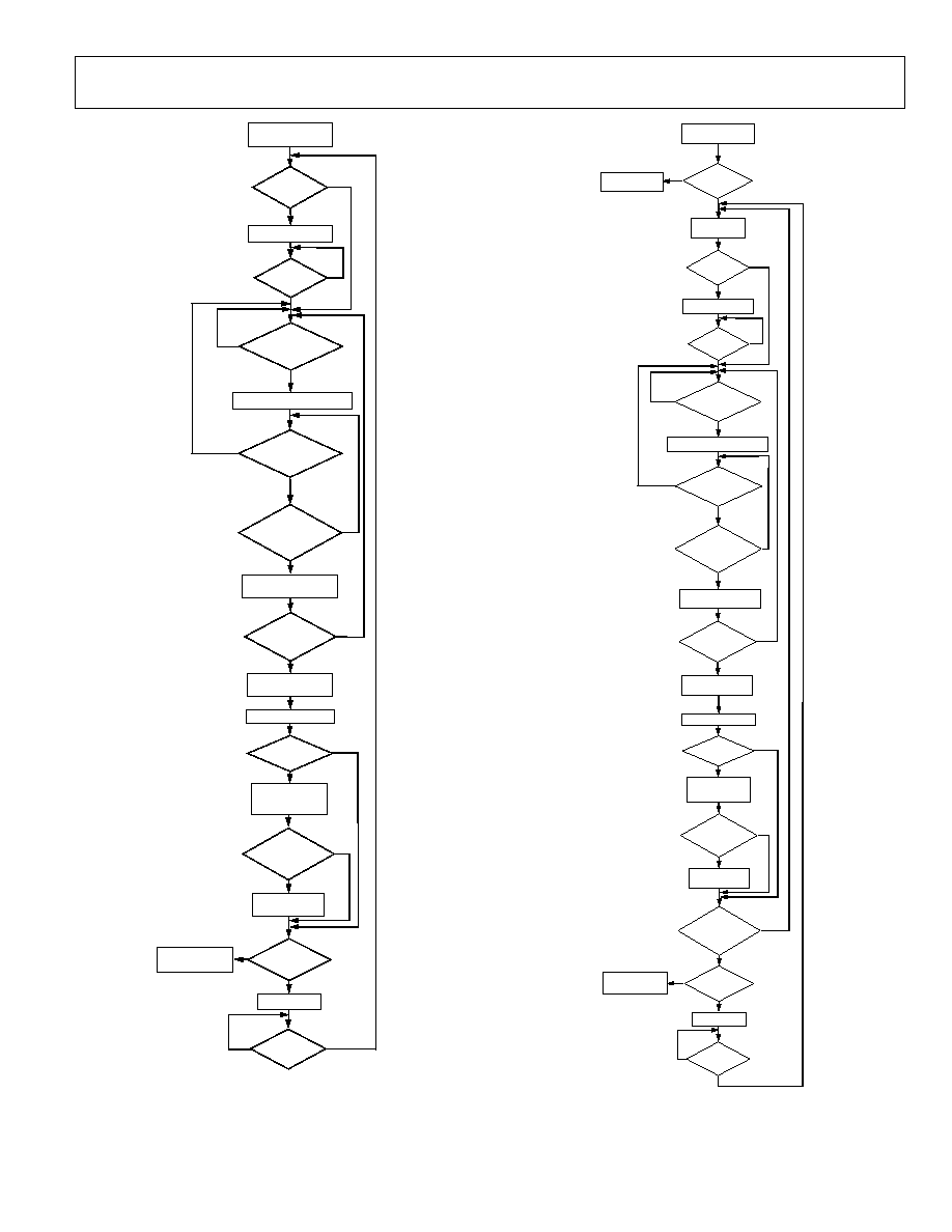
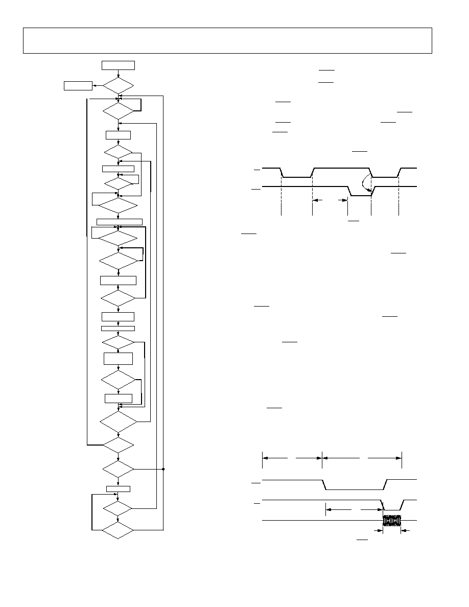
Figure 37. Single Channel Operation
03796-017
YES
NO
ONCE-ONLY
MODE?
GOTO MODE 00
TIMER
FINISHED?
START TIMER
NO
YES
*NOTE: SEE EXPLANATION IN TEXT
LIMIT COMPARISON
START FCD TIMER
UPDATE ALERT
ENABLE/STATUS
REGISTER
CONVERT
SELECTED CHANNEL
IS FCD
FINISHED?
HOST PROGRAMS
AD7877 IN MODE 10
NO
YES
NO
YES
NO
YES
YES
NO
IS AVERAGING
FINISHED?
WRITE RESULT TO
REGISTERS
ALERT
SOURCE
ENABLED?
IS ACQUISITION
TIME FINISHED?
IS FCD
REQUIRED?
START ACQUISITION TIMER
OUT-OF-LIMIT?
ASSERT ALERT
OUTPUT*
YES
NO
YES
NO
VALID
SEQUENCE 0?
SELECT NEXT
CHANNEL
GOTO MODE 00
LAST CHANNEL
IN SEQUENCE?
YES
NO
YES
IS STOPACQ
SIGNAL ACTIVE?
NO
YES
IS STOPACQ
SIGNAL ACTIVE?
YES
NO
NO
Figure 38. Slave Mode Sequencer Operation
AD7877
Rev. A | Page 24 of 44
03796-018
YES
NO
ONCE-ONLY
MODE?
TIMER
FINISHED?
START TIMER
NO
YES
*NOTE: SEE EXPLANATION IN TEXT
LIMIT COMPARISON
START FCD TIMER
UPDATE ALERT
ENABLE/STATUS
REGISTER
CONVERT
SELECTED CHANNEL
IS FCD
FINISHED?
NO
YES
NO
YES
NO
YES
YES
NO
IS AVERAGING
FINISHED?
WRITE RESULT TO
REGISTERS
ALERT
SOURCE
ENABLED?
IS ACQUISITION
TIME FINISHED?
IS FCD
REQUIRED?
START ACQUISITION TIMER
OUT-OF-LIMIT?
ASSERT ALERT
OUTPUT*
YES
NO
YES
NO
VALID
SEQUENCE 1?
SELECT NEXT
CHANNEL
GOTO MODE 00
LAST CHANNEL
IN SEQUENCE?
YES
IS
SCREEN
TOUCHED?
NO
YES
YES
NO
IS STOPACQ
SIGNAL ACTIVE?
IS STOPACQ
SIGNAL ACTIVE?
NO
YES
YES
NO
IS
SCREEN STILL
TOUCHED?
YES
IS
SCREEN STILL
TOUCHED?
YES
NO
NO
NO
HOST PROGRAMS
AD7877 IN MODE 11
Figure 39. Master Mode Sequencer Operation
INTERRUPTS
Data Available Output (DAV)
The data available output (DAV) indicates that new ADC data is
available in the results registers. While the ADC is idle or is
converting, DAV is high. Once the ADC has finished converting
and new data has been written to the results registers, DAV goes
low. Taking DAV low to read the registers resets DAV to a high
condition. DAV is also reset, if a new conversion is started by
the AD7877 because the timer expired. The host should attempt
to read the results registers only while DAV is low.
03796-019
CS
DAV
AD7877
STATUS
IDLE
SETUP
BY HOST
ADC
CONVERTING
NEW DATA
AVAILABLE
HOST READS
RESULTS
IDLE
t
CONV
Figure 40. Operation of DAV Output
DAV is useful as a host interrupt in master mode. In this mode,
the host can program the AD7877 to automatically perform a
sequence of conversions, and can be interrupted by DAV at the
end of each conversion sequence.
When the on-board timer is programmed to perform automatic
conversions, a limited time is available to the host to read the
results registers before another sequence of conversions begins.
The DAV signal is reset high when the timer expires, and the
host should not access the results registers while DAV is high.
Figure 41 shows the worst-case timings for reading the results
registers after DAV has gone low. The timer is set at a minimum,
and the conversion sequence includes all eleven possible ADC
channels. t
1
is the time taken for acquisition and conversion on
one ADC channel. t
2
shows the minimum timer delay, which is
1024 clock periods. t
3
is the time taken to read all 11 result
registers. If the host wants to read all 11 registers, then it must
do so before the timer expires. t
4
is the maximum time allowable
between DAV going low and the host beginning to read the
results registers. If t
4
is exceeded, then all registers cannot be
read before the start of a new conversion, and incorrect data
could be read by the host.
03796-020
DOUT
AD7877
STATUS
CHANNEL 11
CONVERSION AND
ACQUISITION
TIMER INTERVAL
CHNL
1
t
1
t
2
t
3
t
4
CS
DAV
Figure 41. Timing for Reads after DAV Goes Low
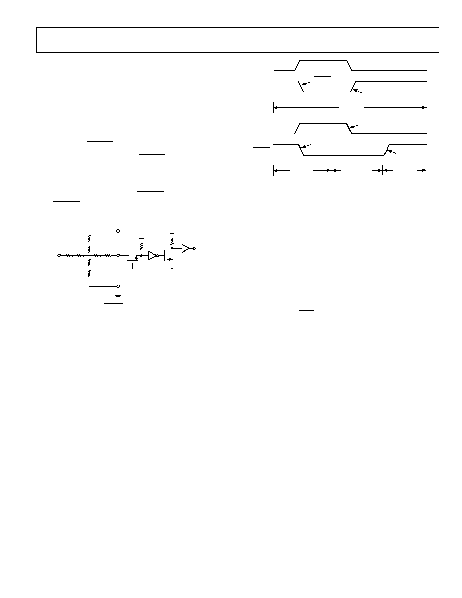
AD7877
Rev. A | Page 25 of 44
If
f
DCLK
= 20 MHz (maximum), then
t
DCLK
= 50 ns.
t
2
=
timer interval ◊ t
DCLK
= (1024 ◊ 50 ns) = 51.2 µs
T
WRITE
=
T
READ
= 16 clk period ◊
t
DCLK
= 800 ns
t
3
= maximum time taken to write read address and read
11 registers = 800 ns (write) + [800 ns (read) ◊ 11] = 9.6 µs.
t
4MAX
=
t
2
-
t
3
= 51.2 µs - 9.6 µs = 41.6 µs
Pen Interrupt (PENIRQ)
The pen interrupt request output (PENIRQ) goes low whenever
the screen is touched. The pen interrupt equivalent output
circuitry is outlined in Figure 42. This is a digital logic output
with an internal pull-up resistor of 50 k, which means it does
not need an external pull-up. The PENIRQ output idles high.
The PENIRQ circuitry is always enabled, except during
conversions.
03796-021
X+
TOUCH
SCREEN
Y+
50k
Y≠
X≠
PENIRQ
ENABLE
PENIRQ
V
CC
V
CC
Figure 42. PENIRQ Output Equivalent Circuit
When the screen is touched, PENIRQ goes low. This can be
used to generate an interrupt request to the host. When the
screen touch ends, PENIRQ goes high immediately, if the ADC
is idle. If the ADC is converting, PENIRQ goes high when the
ADC becomes idle. The PENIRQ operation for these two
conditions is shown in Figure 43.
03796-
022
SCREEN
PENIRQ
ADC
STATUS
TOUCHED
NOT
TOUCHED
NOT
TOUCHED
NOT
TOUCHED
NOT
TOUCHED
ADC IDLE
SCREEN
PENIRQ
ADC
STATUS
TOUCHED
ADC IDLE
ADC
CONVERTING
ADC IDLE
RELEASE NOT
DETECTED
PENIRQ
DETECTS
RELEASE
PENIRQ
DETECTS
RELEASE
PENIRQ
DETECTS
TOUCH
PENIRQ
DETECTS
TOUCH
Figure 43. PENIRQ Operation for ADC Idle and ADC Converting
SYNCRONIZING THE AD7877 TO THE HOST CPU
The two suggested methods for synchronizing the AD7877 to
its host CPU are slave mode, in which the mode bits can be
either 01b or 10b, and master mode, in which the mode bits
are 11b.
In slave mode, PENIRQ can be used as an interrupt to the host.
When PENIRQ goes low to indicate that the screen has been
touched, the host is awakened. The host can then program the
AD7877 to begin converting in either mode 01b or 10b, and can
read the result registers after the conversions have completed.
In master mode, DAV can also be used as an interrupt to the
host. However, the host should first initialize the AD7877 in
mode 11b. The host can then go into sleep mode to conserve
power. The wake-up on touch feature of the AD7877 is active in
this mode, so, when the screen is touched, the programmed
sequence of conversions begins automatically. When the DAV
signal asserts, the host reads the new data available in the
AD7877 results registers and returns to sleep mode. This
method can significantly reduce the load on the host.
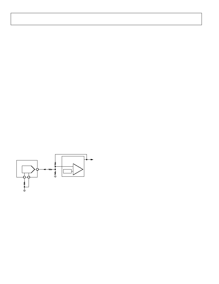
AD7877
Rev. A | Page 26 of 44
8-BIT DAC
The AD7877 features an on-chip 8-bit DAC for LCD contrast
control. The DAC can be configured for voltage output by
clearing Bit 2 of the DAC register (Address 1110b), or for
current output by setting this bit.
The output voltage range can be set to 0 - V
CC
/2 by clearing
Bit 0 of the DAC register, or to 0 - V
CC
by setting this bit. In
current mode, the output range is selectable by an external
resistor, R
RNG
, connected between the ARNG pin and GND. This
sets the full-scale output current according to the following
equations:
I
FS
=
V
CC
/(
R
RNG
◊ 6)
so
R
RNG
=
V
CC
/(
I
FS
◊ 6)
In current mode, the DAC sinks current, that is, positive current
flows into ground. The maximum output current is 1000 µA.
The DAC is updated by writing to Address 1110b of the DAC
register. The 8 MSBs of the data-word are used for DAC data.
The most effective way to control LCD contrast with the DAC is
to use it to control the feedback loop of the dc-dc converter that
supplies the LCD bias voltage, as shown in Figure 44. The bias
voltage for graphic LCDs is typically in the range of 20 V to
25 V, and the dc≠dc converter usually has a feedback loop that
attenuates the output voltage and compares it with an internal
reference voltage.
03796-023
DC-DC
CONVERTER
V
FB
V
OUT
TO LCD
8-BIT
DAC
AD7877
ARNG
R
RNG
1
GND
NOTES:
1
R
RNG
IS REQUIRED ONLY IF DAC IS IN CURRENT MODE.
2
R1 IS REQUIRED ONLY IF DAC IS IN VOLTAGE MODE.
AOUT
R1
2
I
OUT
R3
R2
COMP
VREF
Figure 44. Using the DAC to Adjust LCD Contrast
The circuit operates as follows. If the DAC is in current mode
when the DAC output is zero, it has no effect on the feedback
loop. Irrespective of what the DAC does, the feedback loop
maintains the voltage across R4, V
FB
, equal to V
REF
, and the
output voltage V
OUT
is
V
REF
◊ (
R2 + R3)/R3
As the DAC output is increased, it increases the feedback
current, so the voltage across R2 and, therefore, the output
voltage also increase. Note that the voltage across R3 does not
change. This is important for calculation of the adjustment
range.
In current mode, it is quite easy to calculate the resistor values
to give the required adjustment range in V
OUT
:
1.
Find the required maximum and minimum values of V
OUT
from the LCD manufacturer's data.
2.
Decide on the current around the feedback loop, which for
reasonable accuracy of the output voltage should be at least
100 times the input bias current of the dc≠dc converter's
comparator.
3.
Calculate R3 using the following equation:
R3 = V
FB
/
I
FB
=
V
REF
/
I
FB
4.
Calculate R2 for the minimum value of V
OUT
, when the
DAC has no effect:
R2 = R3(V
OUT(MIN)
-
V
REF
)/
V
REF
5.
Because the voltage across R3 does not change, subtract
V
REF
from V
OUTMAX
and V
OUTMIN
to get the maximum and
minimum voltages across R2.
6.
Calculate the change in feedback current between
minimum and maximum output voltages:
I = V
R2(MAX)
/
R2 - V
R2(MIN)
/
R2
This is the required full-scale current of the DAC.
7.
Calculate R
RNG
from the equation given previously.
Example:
1.
V
CC
= 5 V.
V
OUT(MIN)
is 20 V and
V
OUT(MAX)
is 25 V.
V
REF
is
1.25 V.
2.
Allow 100 µA around the feedback loop.
3.
R3 = 1.25 V/100 µA = 12.5 k. Use the nearest preferred
value of 12 k and recalculate the feedback current as
I
FB
= 1.25 V/12 k = 104 µA
4.
R2 = (20 V - 1.25 V)/104 µA = 180 k.
5.
I = 23.75 V/180 k - 18.75 V/180 k = 28 µA.
6.
R
RNG
= 5 V/(6 ◊ 28 µA) = 30 k.
In voltage mode, the circuit operation depends on whether the
maximum output voltage of the DAC exceeds the dc≠dc
converter V
REF
.
When the DAC output voltage is zero, it sinks the maximum
current through R1. The feedback current, and, therefore, V
OUT
are at their maximum. As the DAC output voltage increases, the
sink current and, therefore, the feedback current decrease, and

AD7877
Rev. A | Page 27 of 44
V
OUT
falls. If the DAC output exceeds V
REF
, it starts to source
current, and V
OUT
has to further decrease to compensate. When
the DAC output is at full scale, V
OUT
is at its minimum.
Note that the effect of the DAC on V
OUT
is opposite in voltage
mode to that in current mode. In current mode, increasing DAC
code increases the sink current, so V
OUT
increases with
increasing DAC code. In voltage mode, increasing DAC code
increases the DAC output voltage, reducing the sink current.
Calculate the resistor values as follows:
1.
Decide on the feedback current as before.
2.
Calculate the parallel combination of R1 and R3 when the
DAC output is zero:
R
P
=
V
REF
/
I
FB
3.
Calculate R2 as before, but use R
P
and V
OUTMAX
:
R2 = R
P
(
V
OUT(MAX)
-
V
REF
)/
V
REF
4.
Calculate the change in feedback current between
minimum and maximum output voltages as before using
I = V
R2(MAX)
/
R2 - V
R2(MIN)
/
R2
This is equal to the change in current through R1 between
zero output and full scale, which is also given by
I = current at zero - current at full scale
=
V/R1 - (V
REF
-
V)/R1
=
V/R1
5.
R1 = V
FS
/
.
6.
Calculate R3 from R1 and R using
R3 = (R1 ◊ R
P
)/(
R1 - R
P
)
Example:
1.
V
CC
= 5 V and
V
FS
=
V
CC
.
V
OUT(MIN)
is 20 V and
V
OUT(MAX)
is
25 V.
V
REF
is 1.25 V. Allow 100 µA around the feedback
loop.
2.
R
P
= 1.25 V/100 µA = 12.5 k.
3.
R2 = 12.5 k ◊ (25 - 1.25 )/1.25 = 237 k.
Use nearest preferred value of 240 k.
4.
I = 25 V/240 k - 20 V/240 k = 21 µA.
5.
R1 = 5 V/21 µA = 238 k.
Use nearest preferred value of 250 k.
6.
R3 = (180 k ◊ 12.5 k)/(180 k - 12.5 k) =13.4 k.
Use nearest preferred value of 13 k.
The actual adjustment range using these values is 21 V to 26 V.
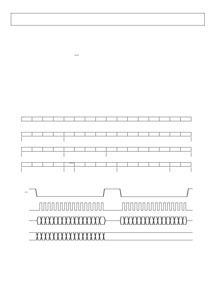
AD7877
Rev. A | Page 28 of 44
SERIAL INTERFACE
The AD7877 is controlled via a 3-wire serial peripheral interface
(SPI). The SPI has a data input pin (DIN) for inputting data to
the device, a data output pin (DOUT) for reading data back
from the device, and a data clock pin (DCLK) for clocking data
into and out of the device. A chip-select pin (CS) enables or
disables the serial interface.
WRITING DATA
Data is written to the AD7877 in 16-bit words. The first four
bits of the word are the register address, which tells the AD7877
which register to write to. The next 12 bits are data. How the
AD7877 handles the data bits depends on the register address.
Register Address 0000b is a dummy address, which does
nothing. Register addresses from 0010b to 1110b are 12-bit
registers that perform various functions as described in the
register map.
Register Address 1111b is not a physical register, but enables an
extended writing mode that allows writing to the GPIO
configuration registers. When the register address is 1111b, the
next four bits of the data-word are the address of a GPIO
configuration register and the eight LSBs are the GPIO configu-
ration data. For details on the configuration of the GPIO pins,
see the General-Purpose I/O Pins section.
Register Address 0001b is a physical register, Control Register 1,
but this is a special register. It contains data for setting up the
ADC channel and operating mode, but Bits 20 to 6 are the
register address for reading. These define which register is read
back during the next read operation. Control Register 1 should
be the last register in the AD7877 to be programmed before
starting a conversion. The three types of data-words used for
writing are shown in Figure 45.
03796-024
D15
D14
D13
D12
D11
D10
D9
D8
D7
D6
D5
D4
D3
D2
D1
D0
16-BIT DATA-WORD
WADD3
WADD2
WADD1
WADD0
D11
D10
D9
D8
D7
D6
D5
D4
D3
D2
D1
D0
WRITING TO A REGISTER
12 BITS DATA
4-BIT REGISTER WRITE ADDRESS
1
1
1
1
EADD3
EADD2
EADD1
EADD0
D7
D6
D5
D4
D3
D2
D1
D0
EXTENDED WRITE OPERATION TO GPIO REGISTERS
8 BITS GPIO DATA
4-BIT EXTENDED ADDRESS
0
0
0
0
SER/DFR CHADD3 CHADD2 CHADD1 CHADD0 RADD4
RADD3
RADD2
RADD1
RADD0
MODE 1 MODE 0
WRITING TO CONTROL REGISTER 1 TO SET ADC CHANNEL, MODE, AND READ REGISTER ADDRESS
ADC CHANNEL ADDRESS
5-BIT READ REGISTER ADDRESS
OPERATING
MODE
EXTENDED WRITE ADDRESS
CONTROL REGISTER 1 ADDRESS
NORMAL (SINGLE-ENDED)/
RATIOMETRIC (DIFFERENTIAL)
CONVERSION
Figure 45. Designation of Data-Word Bits in AD7877 Write Operations
0
3796-025
DCLK
DOUT
1
DIN
2
CS
NOTES:
1
DATA IS CLOCKED OUT ON THE FALLING EDGE OF DCLK.
2
INPUT DATA IS SAMPLED ON THE RISING EDGE OF DCLK.
3
FOR 8-BIT REGISTERS, 8 LEADING ZEROS PRECEDE 8 BITS OF DATA.
4
REGISTER READ ADDRESS INCREMENTS AUTOMATICALLY, PROVIDED THAT A NEW ADDRESS IS NOT WRITTEN TO CONTROL REGISTER 1.
HIGH-Z
HIGH-Z
1
16
1
REGISTER n + 1 DATA
4
REGISTER n DATA
4
0000 + 12-BIT DATA
3
0000 + 12-BIT DATA
3
4-BIT ADDRESS + 12-BIT DATA
D15
D0
D15
D0
D15
D0
16
Figure 46. Overall Read/Write Timing

AD7877
Rev. A | Page 29 of 44
WRITE TIMING
No serial interface operations can take place while CS is high.
To write to the AD7877, CS must be taken low. To write to the
device, a burst of 16 clock pulses is input to DCLK while the
write data is input to DIN. Data is clocked in on the rising edge
of DCLK. If multiple write operations are to be performed, CS
must be taken high after the end of each write operation before
another write operation can be performed by taking CS low
again.
READING DATA
Data is available on the DOUT pin following the falling edge of
CS, when the device is being clocked. The MSB is clocked out
on the falling edge of CS, with subsequent data bits clocked out
on the falling edge of DCLK.
After CS is taken low and the device is clocked, the AD7877
outputs data from the register whose read address is currently
stored in Control Register 1. Once this data has been output, the
address increments automatically. CS must be taken high
between reads. When CS is taken low again, reading continues
from the register whose read address is in Control Register 1,
provided that a write operation does not change the address. If
the register read address reaches 11111b, it is then reset to zero.
This feature allows all registers to be read out in sequence
without having to explicitly write all their addresses to the
device.
Note that because data-words are 16 bits long, but the data
registers are only 12 bits long, or 8 bits in the case of GPIO
registers, the first four bits of a readback data-word are zeros, or
the first 8 bits in the case of a GPIO register.
V
DRIVE
PIN
The supply voltage to all pins associated with the serial interface
(DAV, DIN, DOUT, DCLK, CS, PENIRQ, and ALERT) is
separate from the main V
CC
supply and is connected to the
V
DRIVE
pin. This allows the AD7877 to be connected directly to
processors whose supply voltage is less than the minimum
operating voltage of the AD7877, in fact, as low as 1.7 V.

AD7877
Rev. A | Page 30 of 44
GENERAL-PURPOSE I/O PINS
The AD7877 has one dedicated general-purpose logic input/
output pin (GPIO4), and any or all of the three auxiliary analog
inputs can also be reconfigured as GPIOs. Associated with the
GPIOs are two 8-bit control registers and one 8-bit data register,
which are accessed using the extended write mode.
As mentioned previously, GPIO registers are written to using
the extended writing mode. The first four bits of the data-word
must be 1111b to access the extended writing map, and the next
four bits are the GPIO register address. This leaves 8 bits for the
GPIO register data, because all GPIO registers are 8 bits.
The GPIO control registers are located at Extended Writing
Map Addresses 0000b and 0001b, and the GPIO data register is
at Address 0010b. GPIO registers are read in the same way as
other registers, by writing a 5-bit address to Control Register 1.
The GPIO registers are located at Read Addresses 11011b to
11101b.
GPIO CONFIGURATION
Each GPIO pin is configured by four bits in one of the GPIO
control registers and has a data bit in the GPIO data register.
The GPIO configuration bits are described in the following
sections and in Table 12. Also see the Detailed Register
Descriptions section.
Enable--EN
These bits enable or disable the GPIO pins. When EN = 0, the
corresponding GPIO pin is configured as the alternate function
(AUX input). The other GPIO configuration bits have no effect,
if the particular GPIO is not enabled. When EN = 1, the pin is
configured as a GPIO pin. GPIO4, which does not have an
alternate function, does not have an EN bit; it is always enabled.
Direction--DIR
These bits set the direction of the GPIO pins. When DIR = 0,
the pin is an output. Setting or clearing the relevant bit in the
GPIO data register outputs a value on the corresponding GPIO
pin. The output value depends on the POL bit.
When DIR = 1, the pin is an input. An input value on the
relevant GPIO pin sets or clears the corresponding bit in the
GPIO data register, depending on the POL bit. A GPIO data
register bit is read-only when DIR = 1 for that GPIO.
Polarity--POL
When POL = 0, the GPIO pin is active low. When POL = 1, the
GPIO pin is active high. How this bit affects the GPIO opera-
tion also depends on the DIR bit.
If POL = 1 and DIR = 1, a 1 at the input pin sets the corre-
sponding GPIO data register bit to 1. A 0 at the input pin clears
the corresponding GPIO data bit to 0.
If POL = 1 and DIR = 0, a 1 in the GPIO data register bit puts a
1 on the corresponding GPIO output pin. A 0 in the GPIO data
register bit puts a 0 on the GPIO output pin.
If POL = 0 and DIR = 1, a 1 at the input pin sets the corre-
sponding GPIO data bit to 0. A 0 at the input pin clears the
corresponding GPIO data bit to 1.
If POL = 0 and DIR = 0, a 1 in the GPIO data register bit puts a
0 on the corresponding GPIO output pin. A 0 in the GPIO data
register bit puts a 1 on the GPIO output pin.
Alert Enable--ALEN
GPIOs can operate as interrupt sources to trigger the ALERT
output. This is controlled by the alert enable (ALEN) bits in the
GPIO configuration registers. When ALEN = 1, the correspond-
ing GPIO can trigger an ALERT. When ALEN = 0, the corre-
sponding GPIO cannot cause the ALERT output to assert.
ALERT is asserted low, if any GPIO data register bit is set when
the GPIO is configured as an input. The GPIO data bit is set, if a
1 appears on the GPIO input pin when POL = 1, or if a 0
appears on the GPIO input pin when POL = 0. Note that
ALERT is triggered only when the GPIO is configured as an
input, that is, when DIR = 1. ALERT can never be triggered by a
GPIO that is configured as an output, that is, DIR = 0.
ALERT Output
The ALERT pin is an alarm or interrupt output that goes low, if
any one of a number of interrupt sources is asserted. The results
of high and low limit comparisons on the AUX1, BAT1, BAT2,
and TEMP1 channels are interrupt sources. An out-of-limit
comparison sets a status bit in the alert status/mask register
(Address 00011b).There are separate status bits for both the
high and low limits on each channel to indicate which limit was
exceeded. The interrupt sources can be masked out by clearing
the corresponding enable bit in this register. There is one enable
bit per channel.
ALERT is also asserted, if an input on a GPIO pin sets a bit in
the GPIO data register, as explained in the previous section.
GPIO interrupts can be disabled by clearing the corresponding
ALEN bit in the GPIO control registers.
The interrupt source can be identified by reading the GPIO data
register and the alert status/enable register. ALERT remains
asserted until the source of the interrupt has been masked out
or removed.
If the ALERT source is a GPIO, then masking out the interrupt
by clearing the corresponding ALEN bit to 0 or removing the
source of the interrupt on the GPIO pin causes ALERT to go
high again.

AD7877
Rev. A | Page 31 of 44
If the ALERT source is an out-of-limit measurement, writing a 0
to the corresponding status bit in the alert status/enable register
causes ALERT to go high. However, the status bit is set to 1
again on the next measurement cycle, if the measurement
remains out of limit. The ALERT source can also be masked by
clearing the relevant bit in the alert status/enable register to 0.
Table 12. GPIO Configuration
EN
DIR
POL
ALEN
Data Bit
1
Pin Voltage
2
ALERT
0 X X X X X X
1 0 0 0 0 1 1
1 0 0 0 1 0 1
1 0 0 1 0 1 1
1 0 0 1 1 0 1
1 0 1 0 0 0 1
1 0 1 0 1 1 1
1 0 1 1 0 0 1
1 0 1 1 1 1 1
1 1 0 0 1 0 1
1 1 0 0 0 1 1
1 1 0 1 1 0 0
1 1 0 1 0 1 1
1 1 1 0 0 0 1
1 1 1 0 1 1 1
1 1 1 1 0 0 1
1 1 1 1 1 1 0
1
Shaded data values indicate that a change in input voltage on the pin causes a change in the data register bit.
2
Shaded pin voltage values indicate that a change in the data register causes a change in the output voltage on the pin.
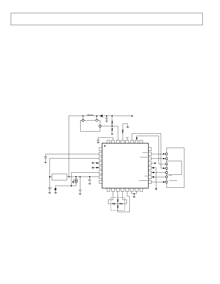
AD7877
Rev. A | Page 32 of 44
GROUNDING AND LAYOUT
It is recommended that the ground pins, AGND and DGND, be
shorted together as close as possible to the device itself on the
user's PCB.
For more information on grounding and layout considerations
for the AD7877, refer to the
Layout and Grounding Recommen-
dations for Touch Screen Digitizers Technical Note.
PCB DESIGN GUIDELINES FOR CHIP SCALE
PACKAGES
The lands on the chip scale package (CP-32) are rectangular.
The printed circuit board pad for these should be 0.1 mm
longer than the package land length and 0.05 mm wider than
the package land width. The land should be centered on the pad.
This ensures that the solder joint size is maximized.
The bottom of the chip scale package has a central thermal pad.
The thermal pad on the printed circuit board should be at least
as large as this exposed pad. On the printed circuit board, there
should be a clearance of at least 0.25 mm between the thermal
pad and the inner edges of the pad pattern. This ensures that
shorting is avoided.
Thermal vias can be used on the printed circuit board thermal
pad to improve thermal performance of the package. If vias are
used, they should be incorporated in the thermal pad at a
1.2 mm pitch grid. The via diameter should be between 0.3 mm
and 0.33 mm and the via barrel should be plated with 1 oz.
copper to plug the via.
The user should connect the printed circuit board thermal pad
to AGND.
03796-026
HOST
NC = NO CONNECT
AD7877
24
NC
21
GPIO4
20
STOPACQ
19
DIN
17
PENIRQ
18
CS
22
ALERT
23
DAV
NC
1
BAT2
2
BAT1
3
AUX3/GPIO3
4
AUX2/GPIO2
5
AUX1/GPIO1
6
V
CC
7
NC
8
NC
32
V
RE
F
31
AOUT
30
ARNG
29
V
DRIV
E
28
DOUT
27
DCLK
26
NC
25
NC
9
X≠
10
Y≠
11
X+
12
Y+
13
AGND
14
DGND
15
NC
16
INT1
SPI
INTE
RFACE
INT2
SCLK
MISO
MOSI
PENIRQ
CS
GPIO
HSYNC SIGNAL
FROM LCD
V
CC
R
RNG
0.1
µ
F
DC-DC
CONVERTER
V
IN
OUT
FB
TO LCD
BACKLIGHT
TOUCH
SCREEN
0.1
µ
F
1.0
µ
F≠10
µ
F
(OPTIONAL)
VOLTAGE
REGULATOR
TEMPERATURE
MEASUREMENT
DIODE
MAIN
BATTERY
SECONDARY
BATTERY
FROM AUDIO
REMOTE CONTROL
FROM
HOTSYNC INPUTS
Figure 47. Typical Application Circuit
AD7877
Rev. A | Page 33 of 44
REGISTER MAPS
Table 13. Write Register Map
Register Address
Binary
WADD3 WADD2 WADD1 WADD0 HEX
Register Name
Description
0
0
0
0
0
None
Unused. Writing to this address has no effect.
0
0
0
1
1
Control Register 1
Contains ADC channel address, register read address, and ADC
mode.
0
0
1
0
2
Control Register 2
Contains ADC averaging, acquisition time, power manage-
ment, first conversion delay, STOPACQ polarity, and reference
and timer settings.
0
0
1
1
3
Alert
Status/Enable
Register
Contains status of high/low limit comparisons for TEMP1, BAT1,
BAT2, and AUX1, and enable bits to allow these channels to
become interrupt sources.
0
1
0
0
4
AUX1 High Limit
User-programmable AUX1 upper limit.
0
1
0
1
5
AUX1 Low Limit
User-programmable AUX1 lower limit.
0
1
1
0
6
BAT1 High Limit
User-programmable BAT1 upper limit.
0
1
1
1
7
BAT1 Low Limit
User-programmable BAT1 lower limit.
1
0
0
0
8
BAT2 High Limit
User-programmable BAT2 upper limit.
1
0
0
1
9
BAT2 Low Limit
User-programmable BAT2 lower limit.
1
0
1
0
A
TEMP1 Low Limit
User-programmable TEMP1 lower limit.
1
0
1
1
B
TEMP1 High Limit
User-programmable TEMP1 upper limit.
1
1
0
0
C
Sequencer
Register 0
Contains channel selection data for slave mode (software)
sequencing.
1
1
0
1
D
Sequencer
Register 1
Contains channel selection data for master mode (hardware)
sequencing.
1
1
1
0
E
DAC Register
Contains DAC data and setup information.
1
1
1
1
F
Extended Write
Not a physical register. Enables writing to extended writing
map.
Table 14. Extended Writing Map
Register Address
Binary
EADD3 EADD2
EADD1
EADD0 HEX
Register Name
Description
0
0
0
0
0
GPIO Control
Register 1
Contains polarity, direction, enabling, and interrupt enabling
settings for GPIO1 and GPIO2.
0
0
0
1
1
GPIO Control
Register 2
Contains polarity, direction, enabling, and interrupt enabling
settings for GPIO3 and GPIO4.
0
0
1
0
2
GPIO Data
Contains GPIO1 to GPIO4 data.

AD7877
Rev. A | Page 34 of 44
Table 15. Read Register Map
Register
Address
Binary
RADD4 RADD3 RADD2 RADD1 RADD0
HEX
Register Name
Description
0
0
0
0
0
00
None
Reads back all zeros.
0
0
0
0
1
01
Control Register 1
See Table 13.
0
0
0
1
0
02
Control Register 2
See Table 13.
0
0
0
1
1
03
Alert Status/Enable
Register
See Table 13.
0
0
1
0
0
04
AUX1 High Limit
See Table 13.
0
0
1
0
1
05
AUX1 Low Limit
See Table 13.
0
0
1
1
0
06
BAT1 High Limit
See Table 13.
0
0
1
1
1
07
BAT1 Low Limit
See Table 13.
0
1
0
0
0
08
BAT2 High Limit
See Table 13.
0
1
0
0
1
09
BAT2 Low Limit
See Table 13.
0
1
0
1
0
0A
TEMP1 Low Limit
See Table 13.
0
1
0
1
1
0B
TEMP1 High Limit
See Table 13.
0
1
1
0
0
0C
Sequencer Register 0
See Table 13.
0
1
1
0
1
0D
Sequencer Register 1
See Table 13.
0
1
1
1
0
0E
DAC Register
See Table 13.
0
1
1
1
1
0F
None
Factory use only.
1
0
0
0
0
10
X+
Measurement at X+ input for Y position.
1
0
0
0
1
11
Y+
Measurement at Y+ input for X position.
1
0
0
1
0
12
Y- (Z2)
Measurement at Y- input for touch-pressure
calculation Z2.
1
0
0
1
1
13
AUX1
Auxiliary Input 1 measurement.
1
0
1
0
0
14
AUX2
Auxiliary Input 2 measurement.
1
0
1
0
1
15
AUX3
Auxiliary Input 3 measurement.
1
0
1
1
0
16
BAT1
Battery Input 1 measurement.
1
0
1
1
1
17
BAT2
Battery Input 1 measurement.
1
1
0
0
0
18
TEMP1
Single-ended temperature measurement.
1
1
0
0
1
19
TEMP2
Differential temperature measurement.
1
1
0
1
0
1A
X+ (Z1)
Measurement at X+ input for touch-pressure
calculation Z1.
1
1
0
1
1
1B
GPIO Control
Register 1
See Table 13.
1
1
1
0
0
1C
GPIO Control
Register 2
See Table 13.
1
1
1
0
1
1D
GPIO Data Register
See Table 13.
1
1
1
1
0
1E
None
Factory use only.
1
1
1
1
1
1F
None
Factory use only.

AD7877
Rev. A | Page 35 of 44
DETAILED REGISTER DESCRIPTIONS
Register Name: Control Register 1
Write Address: 0001; Read Address: 00001; Default Value: 0x000; Type: Read/Write.
Table 16.
Bit
Name
Read/
Write
Description
0
MODE0
R/W
LSB of ADC mode code
1
MODE1
R/W
MSB of ADC mode code
00 = No conversion
01 = Single conversion
10 = Conversion sequence (slave mode)
11 = Conversion sequence (master mode)
2
RD0
R/W
LSB of register read address. To read a register, its address must first be written to Control Register 1.
3
RD1
R/W
Bit 1 of register read address. To read a register, its address must first be written to Control Register 1.
4
RD2
R/W
Bit 2 of register read address. To read a register, its address must first be written to Control Register 1.
5
RD3
R/W
Bit 3 of register read address. To read a register, its address must first be written to Control Register 1.
6
RD4
R/W
MSB of register read address. To read a register, its address must first be written to Control Register 1.
7
CHADD0
R/W
LSB of ADC channel address
8
CHADD1
R/W
Bit 1 of ADC channel address
9
CHADD2
R/W
Bit 2 of ADC channel address
10
CHADD3
R/W
MSB of ADC channel address
0000 = X+ input (Y position)
0001 = Y+ input (X position)
0010 = Y- (Z2) input (used for touch-pressure calculation)
0011 = Auxiliary Input 1 (AUX1)
0100 = Auxiliary Input 2 (AUX2)
0101 = Auxiliary Input 3 (AUX3)
0110 = Battery Monitor Input 1 (BAT1)
0111 = Battery Monitor Input 2 (BAT2)
1000 = Temperature Measurement 1 (used for single conversion)
1001 = Temperature Measurement 2 (used for differential measurement method)
1010 = X+ (Z1) input (used for touch-pressure calculation)
11
SER/DFR
R/W
Selects normal (single-ended) or ratiometric (differential) conversion
0 = Ratiometric (differential)
1 = Normal (single-ended)

AD7877
Rev. A | Page 36 of 44
Register Name: Control Register 2
Write Address: 0010; Read Address: 00010; Default Value: 0x000.
Table 17.
Bit Name
Read/
Write
Description
0
TMR0
R/W
LSB of conversion interval timer
1
TMR1
R/W
MSB of conversion interval timer
00 = Convert only once
01 = Every 1024 clock periods (512 µs)
10 = Every 2048 clock periods (1.024 ms)
11 = Every 16384 clock periods (8.19 ms)
2
REF
R/W
Selects internal or external reference
0 = Internal reference
1 = External reference
3
POL
R/W
Indicates polarity of signal on STOPACQ pin
0 = Active low
1 = Active high
4
FCD0
R/W
LSB of first conversion delay
5
FCD1
R/W
MSB of first conversion delay
This delay occurs before the first conversion after powering up the ADC, before converting the X and Y
coordinate channels to allow settling, and after the last conversion to allow PENIRQ precharge.
00 = 1 clock period delay (500 ns)
01 = 256 clock periods delay (128 µs)
10 = 2048 clock periods delay (1.024 ms)
11 = 16384 clock periods delay (8.19 ms)
6
PM0
R/W
LSB of ADC power management code
7
PM1
R/W
MSB of ADC power management code
00 = ADC and reference powered down continuously
01 = ADC and reference* powered down when not converting
10 = ADC and reference* powered up continuously
11 = ADC powered down when not converting, reference* powered up
*Irrespective of PM bits, reference is always powered down, if REF bit is 1.
8
ACQ0
R/W
LSB of ADC acquisition time
9
ACQ1
R/W
MSB of ADC acquisition time
00 = 4 clock periods (2 µs)
01 = 8 clock periods (4 µs)
10 = 16 clock periods (8 µs)
11 = 32 clock periods (16 µs)
10
AVG0
R/W
LSB of ADC averaging code
11
AVG1
R/W
MSB of ADC averaging code
00 = No averaging (1 conversion per channel)
01 = 4 measurements per channel averaged
10 = 8 measurements per channel averaged
11 = 16 measurements per channel averaged
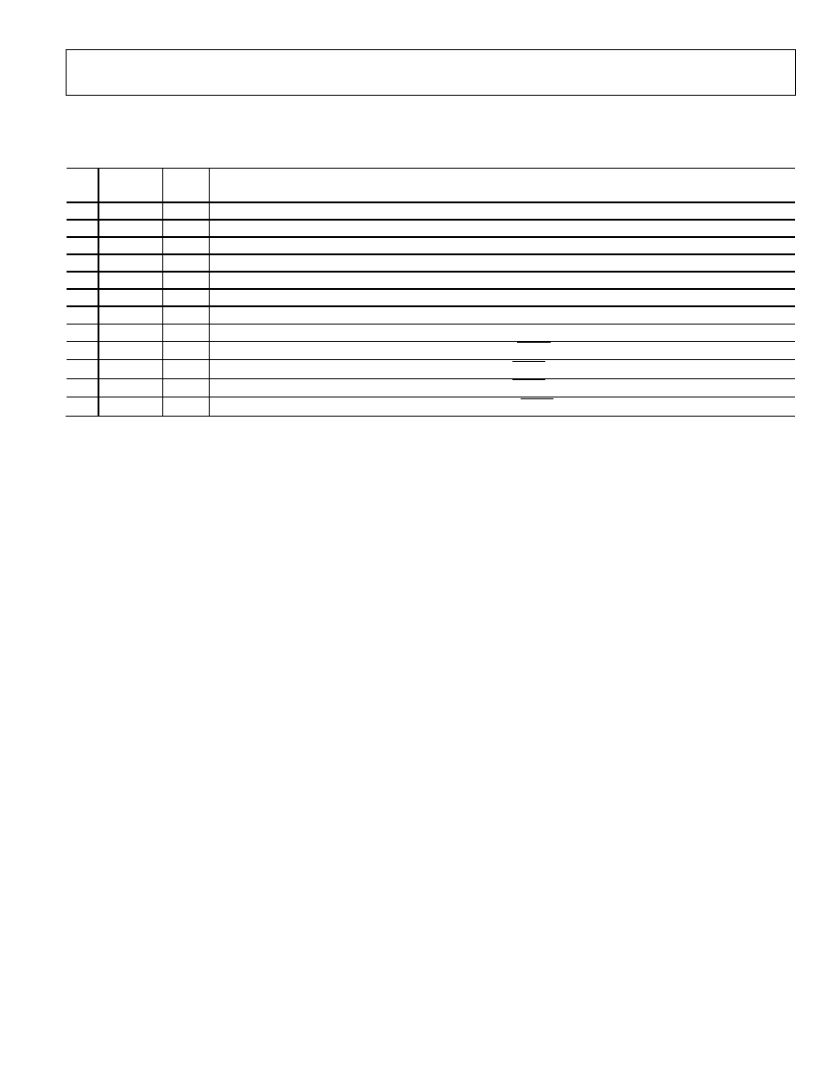
AD7877
Rev. A | Page 37 of 44
Register Name: Alert Status/Enable Register
Write Address: 0011; Read Address: 00011; Default Value: 0x000.
Table 18.
Bit
Name
Read/
Write
Description
0
AUX1LO
R/W
When this bit is 1, the AUX1 channel is below its low limit.
1
BAT1LO
R/W
When this bit is 1, the BAT1 channel is below its low limit.
2
BAT2LO
R/W
When this bit is 1, the BAT2 channel is below its low limit.
3
TEMP1HI
R/W
When this bit is 1, the TEMP1 channel is below its high limit.
4
AUX1HI
R/W
When this bit is 1, the AUX1 channel is above its high limit.
5
BAT1HI
R/W
When this bit is 1, the BAT1 channel is above its high limit.
6
BAT2HI
R/W
When this bit is 1, the BAT2 channel is above its high limit.
7
TEMP1LO R/W
When this bit is 1, the TEMP1 channel is above its low limit.
8
AUX1EN
R/W
Setting this bit enables AUX1 as an interrupt source to the ALERT output.
9
BAT1EN
R/W
Setting this bit enables BAT1 as an interrupt source to the ALERT output.
10
BAT2EN
R/W
Setting this bit enables BAT2 as an interrupt source to the ALERT output.
11
TEMP1EN R/W
Setting this bit enables TEMP1 as an interrupt source to the ALERT output.
Register Name: AUX1 High Limit
Write Address: 0100; Read Address: 00100; Default Value: 0x000; Type: Read/Write.
This register contains the 12-bit high limit for Auxiliary Input 1.
Register Name: AUX1 Low Limit
Write Address: 0101; Read Address: 00101; Default Value: 0x000; Type: Read/Write.
This register contains the 12-bit low limit for Auxiliary Input 1.
Register Name: BAT1 High Limit
Write Address: 0110; Read Address: 00110; Default Value: 0x000; Type: Read/Write.
This register contains the 12-bit high limit for Battery Monitoring Input 1.
Register Name: BAT1 Low Limit
Write Address: 0111; Read Address: 00111; Default Value: 0x000; Type: Read/Write.
This register contains the 12-bit low limit for Battery Monitoring Input 1.
Register Name: BAT2 High Limit
Write Address: 1000; Read Address: 01000; Default Value: 0x000; Type: Read/Write.
This register contains the 12-bit high limit for Battery Monitoring Input 2.
Register Name: BAT2 Low Limit
Write Address: 1001; Read Address: 01001; Default Value: 0x000; Type: Read/Write.
This register contains the 12-bit low limit for Battery Monitoring Input 2.
Register Name: TEMP1 Low Limit
Write Address: 1010; Read Address: 01010; Default Value: 0x000; Type: Read/Write.
This register contains the 12-bit low limit for temperature measurement.
Register Name: TEMP1 High Limit
Write Address: 1011; Read Address: 01011; Default Value: 0x000; Type: Read/Write.
This register contains the 12-bit high limit for temperature measurement.

AD7877
Rev. A | Page 38 of 44
Register Name: Sequencer Register 0
Write Address: 1100; Read Address: 01100; Default Value: 0x000.
Table 19.
Bit Name
Read/
Write
Description
0
Not Used
R/W
This bit is not used.
1
Z1_SS
R/W
Setting this bit includes the Z1 touch-pressure measurement (X+ input) in a slave mode sequence.
2
TEMP2_SS R/W
Setting this bit includes a temperature measurement using differential conversion in a slave mode sequence.
3
TEMP1_SS R/W
Setting this bit includes a temperature measurement using single-ended conversion in a slave mode
sequence.
4
BAT2_SS
R/W
Setting this bit includes measurement of Battery Monitor Input 2 in a slave mode sequence.
5
BAT1_SS
R/W
Setting this bit includes measurement of Battery Monitor Input 1 in a slave mode sequence.
6
AUX3_SS
R/W
Setting this bit includes measurement of Auxiliary Input 3 in a slave mode sequence.
7
AUX2_SS
R/W
Setting this bit includes measurement of Auxiliary Input 2 in a slave mode sequence.
8
AUX1_SS
R/W
Setting this bit includes measurement of Auxiliary Input 1 in a slave mode sequence.
9
Z2_SS
R/W
Setting this bit includes the Z2 touch-pressure measurement (Y- input) in a slave mode sequence.
10
XPOS_SS
R/W
Setting this bit includes measurement of the X position (Y+ input) in a slave mode sequence.
11
YPOS_SS
R/W
Setting this bit includes measurement of the Y position (X+ input) in a slave mode sequence.
Register Name: Sequencer Register 1
Write Address: 1101; Read Address: 01101; Default Value: 0x000.
Table 20.
Bit Name
Read/
Write
Description
0
Not Used
R/W
This bit is not used.
1
Z1_MS
R/W
Setting this bit includes the Z1 touch-pressure measurement (X+ input) in a master mode sequence.
2
TEMP2_MS R/W
Setting this bit includes a temperature measurement using differential conversion in a master mode
sequence.
3
TEMP1_MS R/W
Setting this bit includes a temperature measurement using single-ended conversion in a master mode
sequence.
4
BAT2_MS
R/W
Setting this bit includes measurement of Battery Monitor Input 2 in a master mode sequence.
5
BAT1_MS
R/W
Setting this bit includes measurement of Battery Monitor Input 1 in a master mode sequence.
6
AUX3_MS
R/W
Setting this bit includes measurement of Auxiliary Input 3 in a master mode sequence.
7
AUX2_MS
R/W
Setting this bit includes measurement of Auxiliary Input 2 in a master mode sequence.
8
AUX1_MS
R/W
Setting this bit includes measurement of Auxiliary Input 1 in a master mode sequence.
9
Z2_MS
R/W
Setting this bit includes the Z2 touch-pressure measurement (Y- input) in a master mode sequence.
10
XPOS_MS
R/W
Setting this bit includes measurement of the X position (Y+ input) in a master mode sequence.
11
YPOS_MS
R/W
Setting this bit includes measurement of the Y position (X+ input) in a master mode sequence.
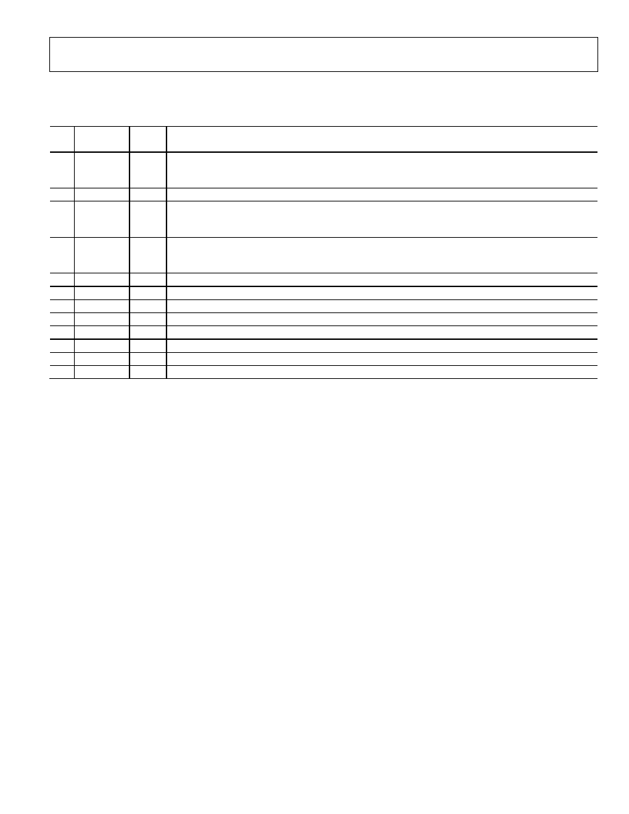
AD7877
Rev. A | Page 39 of 44
Register Name: DAC Register
Write Address: 1110; Read Address: 01110; Default Value: 0x000.
Table 21.
Bit
Name
Read/
Write
Description
0
RANGE
R/W
Output range of the DAC in voltage mode
0 = 0 to V
CC
/2
1 = 0 to V
CC
1
Not Used
R/W
This bit is not used.
2
V/I
R/W
Voltage output and current output
0 = Voltage
1 = Current
3
PD
R/W
DAC power-down
0 = DAC on
1 = DAC powered down
4
DAC0
LSB of DAC data
5
DAC1
Bit 1 of DAC data
6
DAC2
Bit 2 of DAC data
7
DAC3
Bit 3 of DAC data
8
DAC4
Bit 4 of DAC data
9
DAC5
Bit 5 of DAC data
10
DAC6
Bit 6 of DAC data
11
DAC7
MSB of DAC data
Register Name: Y Position
Write Address: N/A; Read Address: 10000; Default Value: 0x000; Type: Read Only.
This register contains the 12-bit result of the measurement at the X+ input with Y layer excited (Y position measurement).
Register Name: X Position
Write Address: N/A; Read Address: 10001; Default Value: 0x000; Type: Read Only.
This register contains the 12-bit result of the measurement at the Y+ input with X layer excited (X position measurement).
Register Name: Z2
Write Address: N/A; Read Address: 10010; Default Value: 0x000; Type: Read Only.
This register contains the 12-bit result of the measurement at the Y- input with excitation voltage applied to Y+ and X- (used for touch-
pressure calculation).
Register Name: AUX1
Write Address: N/A; Read Address: 10011; Default Value: 0x000; Type: Read Only.
This register continues the 12-bit result of the measurement at Auxiliary Input 1.
Register Name: AUX2
Write Address: N/A; Read Address: 10100; Default Value: 0x000; Type: Read Only.
This register continues the 12-bit result of the measurement at Auxiliary Input 2.
Register Name: AUX3
Write Address: N/A; Read Address: 10101; Default Value: 0x000; Type: Read Only.
This register continues the 12-bit result of the measurement at Auxiliary Input 3.

AD7877
Rev. A | Page 40 of 44
Register Name: BAT1
Write Address: N/A; Read Address: 10110; Default Value: 0x000; Type: Read Only.
This register continues the 12-bit result of the measurement at Battery Monitor Input 1.
Register Name: BAT2
Write Address: N/A; Read Address: 10111; Default Value: 0x000; Type: Read Only.
This register continues the 12-bit result of the measurement at Battery Monitor Input 2.
Register Name: TEMP1
Write Address: N/A; Read Address: 11000; Default Value: 0x000; Type: Read Only.
This register continues the 12-bit result of a temperature measurement using single-ended conversion.
Register Name: TEMP2
Write Address: N/A; Read Address: 11001; Default Value: 0x000; Type: Read Only.
This register continues the 12-bit result of a temperature measurement using a differential conversion.
Register Name: Z1
Write Address: N/A; Read Address: 11010; Default Value: 0x000; Type: Read Only.
This register continues the 12-bit result of a measurement at the X+ input with excitation voltage applied to Y+ and X- (used for touch-
pressure calculation).
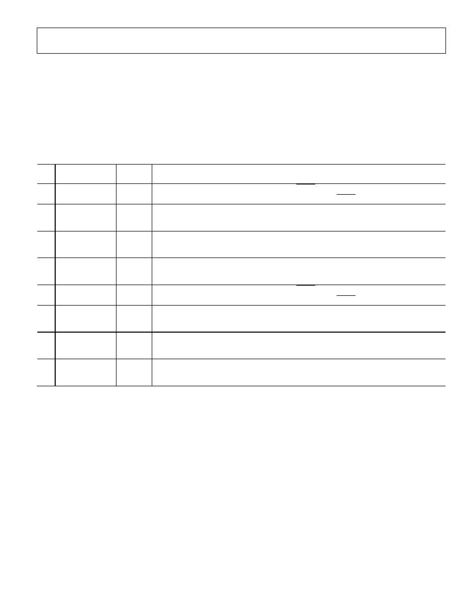
AD7877
Rev. A | Page 41 of 44
GPIO REGISTERS
GPIO registers are written to using an extended 8-bit address.
The first four bits of the data-word are always 1111b to access
the extended writing map. The next four bits are the register
address. This leaves 8 bits for the GPIO data.
GPIO registers are read like all other registers, by writing a 5-bit
address to Control Register 1, then reading DOUT.
See the GPIO Configuration section for information on
configuring the GPIOs.
Register Name: GPIO Control Register 1
Write Address: [1111] 0000; Read Address: 11011; Default Value: 0x000.
Table 22.
Bit
Name
Read/
Write
Description
0
GPIO2_ALEN
R/W
If this bit is 1, GPIO2 is an interrupt source for the ALERT output.
Clearing this bit masks out GPIO2 as an interrupt source for the ALERT output.
1
GPIO2_DIR
R/W
This bit sets the direction of GPIO2.
0 = Output
1 = Input
2
GPIO2_POL
R/W
This bit determines if GPIO2 is active high or low.
0 = Active low
1 = Active high
3
GPIO2_EN
R/W
This bit selects the function of AUX2/GPIO2.
0 = AUX2
1 = GPIO2
4
GPIO1_ALEN
R/W
If this bit is 1, GPIO1 is an interrupt source for the ALERT output.
Clearing this bit masks out GPIO1 as an interrupt source for the ALERT output.
5
GPIO1_DIR
R/W
This bit sets the direction of GPIO1.
0 = Output
1 = Input
6
GPIO1_POL
R/W
This bit determines if GPIO1 is active high or low.
0 = Active low
1 = Active high
7
GPIO1_EN
R/W
This bit selects the function of AUX1/GPIO1.
0 = AUX1
1 = GPIO1
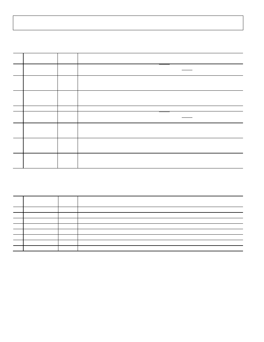
AD7877
Rev. A | Page 42 of 44
Register Name: GPIO Control Register 2
Write Address: [1111] 0001; Read Address: 11100; Default Value: 0x000.
Table 23.
Bit
Name
Read/
Write
Description
0
GPIO4_ALEN
R/W
If this bit is 1, GPIO4 is an interrupt source for the ALERT output.
Clearing this bit masks out GPIO3 as an interrupt source for the ALERT output.
1
GPIO4_DIR
R/W
This bit sets the direction of GPIO4.
0 = Output
1 = Input
2
GPIO4_POL
R/W
This bit determines if GPIO4 is active high or low.
0 = Active low
1 = Active high
3
Not Used
This bit is not used.
4
GPIO3_ALEN
R/W
If this bit is 1, GPIO3 is an interrupt source for the ALERT output.
Clearing this bit masks out GPIO4 as an interrupt source for the ALERT output.
5
GPIO3_DIR
R/W
This bit sets the direction of GPIO3.
0 = Output
1 = Input
6
GPIO3_POL
R/W
This bit determines if GPIO3 is active high or low.
0 = Active low
1 = Active high
7
GPIO3_EN
R/W
This bit selects the function of AUX3/GPIO3.
0 = AUX3
1 = GPIO3
Register Name: GPIO Data Register
Write Address: [1111] 0010; Read Address: 11101; Default Value: 0x000.
Table 24.
Bit
Name
Read/
Write
Description
0
Not Used
This bit is not used.
1
Not Used
This bit is not used.
2
Not Used
This bit is not used.
3
Not Used
This bit is not used.
4
GPIO4_DAT
R/W
GPIO4 data bit.
5
GPIO3_DAT
R/W
GPIO3 data bit.
6
GPIO2_DAT
R/W
GPIO2 data bit.
7
GPIO1_DAT
R/W
GPIO1 data bit.
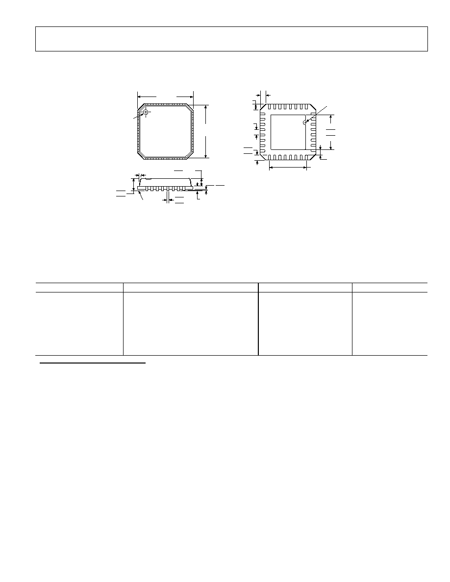
AD7877
Rev. A | Page 43 of 44
OUTLINE DIMENSIONS
COMPLIANT TO JEDEC STANDARDS MO-220-VHHD-2
0.30
0.23
0.18
0.20 REF
0.80 MAX
0.65 TYP
0.05 MAX
0.02 NOM
12∞ MAX
1.00
0.85
0.80
SEATING
PLANE
COPLANARITY
0.08
1
32
8
9
25
24
16
17
0.50
0.40
0.30
3.50 REF
0.50
BSC
PIN 1
INDICATOR
TOP
VIEW
5.00
BSC SQ
4.75
BSC SQ
3.25
3.10 SQ
2.95
PIN 1
INDICATOR
0.60 MAX
0.60 MAX
0.25 MIN
EXPOSED
PAD
(BOTTOM VIEW)
Figure 48. 32-Lead Lead Frame Chip Scale Package [LFCSP]
5 mm ◊ 5 mm Body
(CP-32-2)
Dimensions shown in millimeters
ORDERING GUIDE
Model
Operating Temperature Range
Package Description
Package Option
AD7877ACP-REEL
-40∞C to +85∞C
32-Lead LFCSP
CP-32-2
AD7877ACP-REEL7
-40∞C to +85∞C
32-Lead LFCSP
CP-32-2
AD7877ACP-500RL7
-40∞C to +85∞C
32-Lead LFCSP
CP-32-2
AD7877ACPZ-REEL
1
-40∞C to +85∞C
32-Lead LFCSP
CP-32-2
AD7877ACPZ-REEL7
1
-40∞C to +85∞C
32-Lead LFCSP
CP-32-2
AD7877ACPZ-500RL7
1
-40∞C to +85∞C
32-Lead LFCSP
CP-32-2
EVAL-AD7877EB
Evaluation Board
1
Z = Pb-free part.

AD7877
Rev. A | Page 44 of 44
NOTES
© 2004 Analog Devices, Inc. All rights reserved. Trademarks and
registered trademarks are the property of their respective owners.
D03796≠0≠11/04(A)