Äîêóìåíòàöèÿ è îïèñàíèÿ www.docs.chipfind.ru
2-Channel, 2.35 V to 5.25 V
250 kSPS, 10-/12-Bit ADCs
AD7911/AD7921
Rev. 0
Information furnished by Analog Devices is believed to be accurate and reliable.
However, no responsibility is assumed by Analog Devices for its use, nor for any
infringements of patents or other rights of third parties that may result from its use.
Specifications subject to change without notice. No license is granted by implication
or otherwise under any patent or patent rights of Analog Devices. Trademarks and
registered trademarks are the property of their respective owners.
One Technology Way, P.O. Box 9106, Norwood, MA 02062-9106, U.S.A.
Tel: 781.329.4700
www.analog.com
Fax: 781.326.8703
© 2004 Analog Devices, Inc. All rights reserved.
FEATURES
Fast throughput rate: 250 kSPS
Specified for V
DD
of 2.35 V to 5.25 V
Low power:
4 mW typ at 250 kSPS with 3 V supplies
13.5 mW typ at 250 kSPS with 5 V supplies
Wide input bandwidth:
71 dB minimum SNR at 100 kHz input frequency
Flexible power/serial clock speed management
No pipeline delays
High speed serial interface:
SPI®/QSPITM/MICROWIRETM/DSP compatible
Standby mode: 1 µA maximum
8-lead TSOT package
8-lead MSOP package
APPLICATIONS
Battery-powered systems:
Personal digital assistants
Medical instruments
Mobile communications
Instrumentation and control systems
Data acquisition systems
High speed modems
Optical sensors
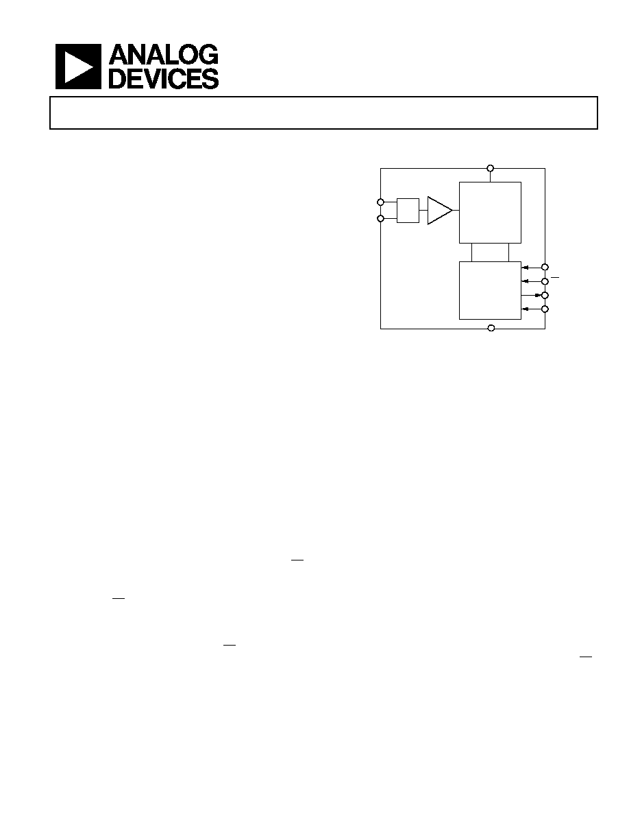
GENERAL DESCRIPTION
The AD7911/AD7921
1
are 10-bit and 12-bit, high speed, low
power, 2-channel successive approximation ADCs, respectively.
The parts operate from a single 2.35 V to 5.25 V power supply
and feature throughput rates of up to 250 kSPS. The parts
contain a low noise, wide bandwidth track-and-hold amplifier,
which can handle input frequencies in excess of 6 MHz. The
conversion process and data acquisition are controlled using CS
and the serial clock, allowing the devices to interface with
microprocessors or DSPs. The input signal is sampled on the
falling edge of CS, and the conversion is also initiated at this
point. There are no pipeline delays associated with the part.
The channel to be converted is selected through the DIN pin,
and the mode of operation is controlled by CS. The serial data
stream from the DOUT pin has a channel identifier bit, which
provides information about the converted channel.
1
Protected by U.S. Patent Number 6,681,332.
FUNCTIONAL BLOCK DIAGRAM
04350-0-001
T/H
CONTROL LOGIC
10-/12-BIT
SUCCESSIVE
APPROXIMATION
ADC
GND
V
DD
AD7911/AD7921
V
IN0
V
IN1
SCLK
DOUT
CS
DIN
MUX
Figure 1.
The AD7911/AD7921 use advanced design techniques to
achieve very low power dissipation at high throughput rates.
The reference for the part is taken internally from V
DD
, thereby
allowing the widest dynamic input range to the ADC. The
analog input range for the part, therefore, is 0 to V
DD
. The
conversion rate is determined by the SCLK signal.
PRODUCT HIGHLIGHTS
1.
2-channel, 250 kSPS, 10-/12-bit ADCs in TSOT package.
2.
Low power consumption.
3.
Flexible power/serial clock speed management.
The conversion rate is determined by the serial clock;
conversion time is reduced when the serial clock speed is
increased. The parts also feature a power-down mode to
maximize power efficiency at lower throughput rates.
Average power consumption is reduced when the power-
down mode is used while not converting. Current
consumption is 1 µA maximum and 50 nA typically when
in power-down mode.
4.
Reference derived from the power supply.
5.
No pipeline delay.
The parts feature a standard successive approximation
ADC with accurate control of the sampling instant via a CS
input and once-off conversion control.

AD7911/AD7921
Rev. 0 | Page 2 of 28
TABLE OF CONTENTS
Specifications..................................................................................... 3
AD7911 Specifications................................................................. 3
AD7921 Specifications................................................................. 5
Timing Specifications .................................................................. 7
Timing Diagrams.......................................................................... 7
Timing Examples.......................................................................... 8
Absolute Maximum Ratings............................................................ 9
ESD Caution.................................................................................. 9
Pin Configurations and Function Descriptions ......................... 10
Terminology .................................................................................... 11
Typical Performance Characteristics ........................................... 13
Circuit Information ........................................................................ 15
Converter Operation.................................................................. 15
ADC Transfer Function............................................................. 15
Typical Connection Diagram ................................................... 16
Analog Input ............................................................................... 16
Digital Inputs .............................................................................. 17
DIN Input .................................................................................... 17
DOUT Output ............................................................................ 17
Modes of Operation ....................................................................... 18
Normal Mode.............................................................................. 18
Power-Down Mode .................................................................... 18
Power-Up Time .......................................................................... 19
Power vs. Throughput Rate....................................................... 20
Serial Interface ................................................................................ 21
Microprocessor Interfacing....................................................... 22
Application Hints ........................................................................... 24
Grounding and Layout .............................................................. 24
Outline Dimensions ....................................................................... 25
Ordering Guide .......................................................................... 25
REVISION HISTORY
Revision 0: Initial Version
AD7911/AD7921
Rev. 0 | Page 3 of 28
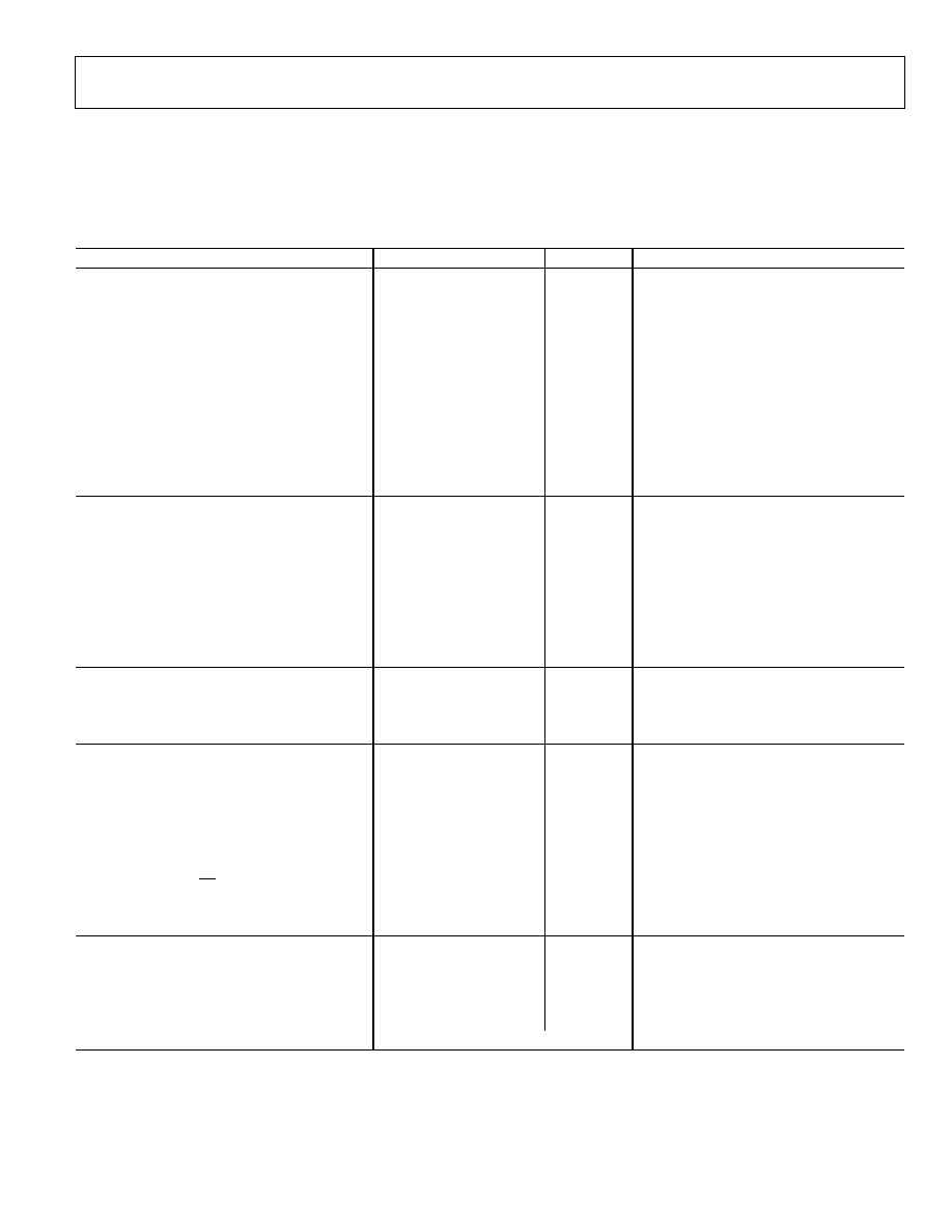
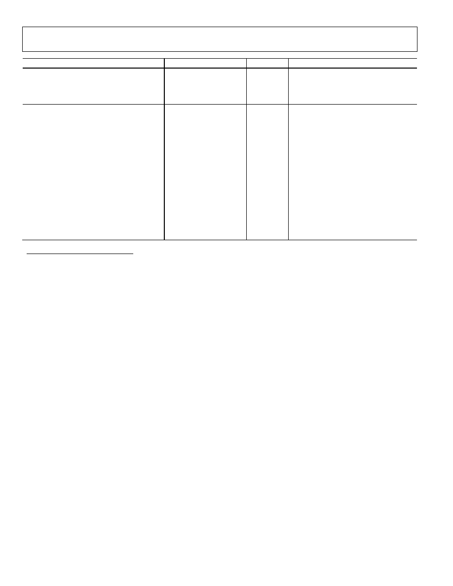
SPECIFICATIONS
AD7911 SPECIFICATIONS
Temperature range for A Grade from -40°C to +85°C.
V
DD
= 2.35 V to 5.25 V, f
SCLK
= 5 MHz, f
SAMPLE
= 250 kSPS; T
A
= T
MIN
to T
MAX
, unless otherwise noted.
Table 1.
Parameter
A Grade
1
Unit
Test Conditions/Comments
DYNAMIC PERFORMANCE
f
IN
= 100 kHz sine wave
Signal-to- Noise and Distortion (SINAD)
2
61
dB min
Total Harmonic Distortion (THD)
2
-71
dB max
Peak Harmonic or Spurious Noise (SFDR)
2
-72
dB max
Intermodulation Distortion (IMD)
2
Second-Order Terms
-82
dB typ
fa = 100.73 kHz, fb = 90.7 kHz
Third-Order Terms
-83
dB typ
fa = 100.73 kHz, fb = 90.7 kHz
Aperture Delay
10
ns typ
Aperture Jitter
30
ps typ
Channel-to-Channel Isolation
2
-90
dB typ
Full Power Bandwidth
8.5
MHz typ
@ 3 dB
1.5
MHz typ
@ 0.1 dB
DC ACCURACY
Resolution
10
Bits
Integral Nonlinearity
2
±0.5
LSB max
Differential Nonlinearity
2
±0.5
LSB max
Guaranteed no missed codes to 10 bits
Offset Error
2
±0.5
LSB max
Offset Error Match
2, 3
±0.3
LSB max
Gain Error
2
±0.5
LSB max
Gain Error Match
2, 3
±0.3
LSB max
Total Unadjusted Error (TUE)
2
±0.5
LSB max
ANALOG INPUT
Input Voltage Ranges
0 to V
DD
V
DC Leakage Current
±0.3
µA max
Input Capacitance
20
pF typ
LOGIC INPUTS
Input High Voltage, V
INH
0.7
(V
DD
)
V min
2.35 V V
DD
2.7 V
2
V min
2.7 V < V
DD
5.25 V
Input Low Voltage, V
INL
0.3
V max
V
DD
= 2.35 V
0.2
(V
DD
)
V max
2.35 V < V
DD
2.7 V
0.8
V max
2.7 V < V
DD
5.25 V
Input Current, I
IN
, SCLK Pin
±0.3
µA max
V
IN
= 0 V or V
DD
Input Current, I
IN
, CS Pin
±0.3 µA
max
Input Current, I
IN
, DIN Pin
±0.3
µA max
Input Capacitance, C
IN
5
pF max
LOGIC OUTPUTS
Output High Voltage, V
OH
V
DD
- 0.2
V min
I
SOURCE
= 200 µA, V
DD
= 2.35 V to 5.25 V
Output Low Voltage, V
OL
0.2
V max
I
SINK
= 200 µA
Floating-State Leakage Current
±0.3
µA max
Floating-State Output Capacitance
3
5
pF max
Output Coding
Straight (natural) binary
See notes at end of table.
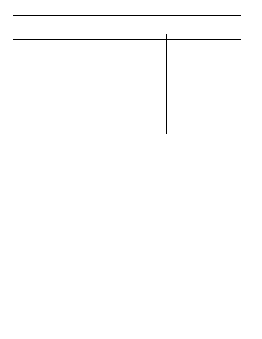
AD7911/AD7921
Rev. 0 | Page 4 of 28
Parameter
A Grade
1
Unit
Test Conditions/Comments
CONVERSION RATE
Conversion Time
2.8
µs max
14 SCLK cycles with SCLK at 5 MHz
Track-and-Hold Acquisition Time
2
290
ns max
Throughput Rate
250
kSPS max
POWER REQUIREMENTS
V
DD
2.35/5.25
V min/max
I
DD
Digital I/Ps = 0 V or V
DD
Normal Mode (Static)
3
mA typ
V
DD
= 4.75 V to 5.25 V, SCLK on or off
1.5
mA typ
V
DD
= 2.35 V to 3.6 V, SCLK on or off
Normal Mode (Operational)
4
mA max
V
DD
= 4.75 V to 5.25 V, f
SAMPLE
= 250 kSPS
2
mA max
V
DD
= 2.35 V to 3.6 V, f
SAMPLE
= 250 kSPS
Full Power-Down Mode (Static)
1
µA max
SCLK on or off, typically 50 nA
Full Power-Down Mode (Dynamic)
0.38
mA typ
V
DD
= 5 V, f
SCLK
= 5 MHz, f
SAMPLE
= 25 kSPS
0.2
mA typ
V
DD
= 3 V, f
SCLK
= 5 MHz, f
SAMPLE
= 25 kSPS
Power Dissipation
4
Normal Mode (Operational)
20
mW max
V
DD
= 5 V, f
SAMPLE
= 250 kSPS
6
mW max
V
DD
= 3 V, f
SAMPLE
= 250 kSPS
Full Power-Down
5
µW max
V
DD
= 5 V
1
Operational from V
DD
= 2 V, with V
IH
= 1.9 V minimum and V
IL
= 0.1 V maximum.
2
See the Terminology section.
3
Guaranteed by characterization.
4
See the Power vs. Throughput Rate section.
AD7911/AD7921
Rev. 0 | Page 5 of 28
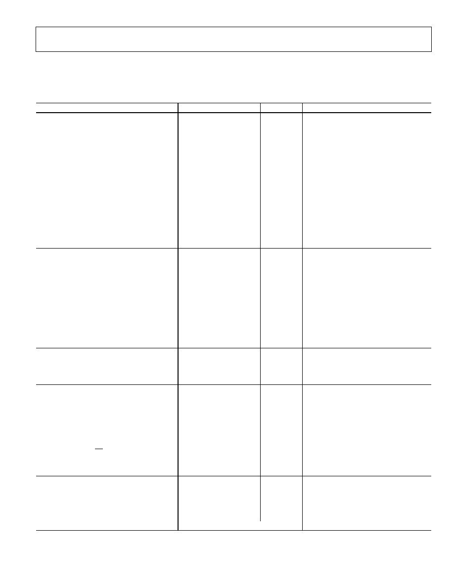
AD7921 SPECIFICATIONS
Temperature range for A Grade from -40°C to +85°C.
V
DD
= 2.35 V to 5.25 V, f
SCLK
= 5 MHz, f
SAMPLE
= 250 kSPS; T
A
= T
MIN
to T
MAX
, unless otherwise noted.
Table 2.
Parameter A
Grade
1
Unit
Test Conditions/Comments
DYNAMIC PERFORMANCE
f
IN
= 100 kHz sine wave
Signal-to-Noise and Distortion (SINAD)
2
70
dB min
72
dB typ
Signal-to-Noise Ratio (SNR)
2
71
dB min
72.5
dB typ
Total Harmonic Distortion (THD)
2
-81
dB typ
Peak Harmonic or Spurious Noise (SFDR)
2
-84
dB typ
Intermodulation Distortion (IMD)
2
Second-Order Terms
-84
dB typ
fa = 100.73 kHz, fb = 90.72 kHz
Third-Order Term
-86
dB typ
fa = 100.73 kHz, fb = 90.72 kHz
Aperture Delay
10
ns typ
Aperture Jitter
30
ps typ
Channel-to-Channel Isolation
2
-90
dB typ
Full Power Bandwidth
8.5
MHz typ
@ 3 dB
1.5
MHz typ
@ 0.1 dB
DC ACCURACY
Resolution 12
Bits
Integral Nonlinearity
2
±1.5
LSB max
Differential Nonlinearity
2
-0.9/+1.5
LSB max
Guaranteed no missed codes to 12 bits
Offset Error
2
±1.5
LSB max
±0.5
LSB
typ
Offset Error Match
2, 3
±0.5
LSB max
Gain Error
2
± 2
LSB max
±0.3
LSB
typ
Gain Error Match
2, 3
±1 LSB
max
Total Unadjusted Error (TUE)
2
±1.5
LSB max
ANALOG INPUT
Input Voltage Ranges
0 to V
DD
V
DC Leakage Current
±0.3
µA max
Input Capacitance
20
pF typ
LOGIC INPUTS
Input High Voltage, V
INH
0.7 (V
DD
)
V min
2.35 V V
DD
2.7 V
2
V min
2.7 V < V
DD
5.25 V
Input Low Voltage, V
INL
0.3
V max
V
DD
= 2.35 V
0.2
(V
DD
)
V max
2.35 V < V
DD
2.7 V
0.8
V max
2.7 V < V
DD
5.25 V
Input Current, I
IN
, SCLK Pin
±0.3
µA max
V
IN
= 0 V or V
DD
Input Current, I
IN
, CS Pin
±0.3 µA
max
Input Current, I
IN
, DIN Pin
±0.3
µA max
Input Capacitance, C
IN
3
5
pF max
LOGIC OUTPUTS
Output High Voltage, V
OH
V
DD
- 0.2
V min
I
SOURCE
= 200 µA; V
DD
= 2.35 V to 5.25 V
Output Low Voltage, V
OL
0.2
V max
I
SINK
= 200 µA
Floating-State Leakage Current
±0.3
µA max
Floating-State Output Capacitance
3
5
pF max
Output Coding
Straight (natural) binary
See notes at end of table.
AD7911/AD7921
Rev. 0 | Page 6 of 28
Parameter A
Grade
1
Unit
Test Conditions/Comments
CONVERSION RATE
Conversion Time
3.2
µs max
16 SCLK cycles with SCLK at 5 MHz
Track-and-Hold Acquisition Time
2
290
ns
max
Throughput Rate
250
kSPS max
See the Serial Interface section
POWER REQUIREMENTS
V
DD
2.35/5.25
V min/max
I
DD
Digital I/Ps = 0 V or V
DD
Normal Mode (Static)
3
mA typ
V
DD
= 4.75 V to 5.25 V, SCLK on or off
1.5
mA typ
V
DD
= 2.35 V to 3.6 V, SCLK on or off
Normal Mode (Operational)
4
mA max
V
DD
= 4.75 V to 5.25 V, f
SAMPLE
= 250 kSPS
2
mA max
V
DD
= 2.35 V to 3.6 V, f
SAMPLE
= 250 kSPS
Full Power-Down Mode (Static)
1
µA max
SCLK on or off, typically 50 nA
Full Power-Down Mode (Dynamic)
0.4
mA typ
V
DD
= 5 V, f
SCLK
= 5 MHz, f
SAMPLE
= 25 kSPS
0.22
mA typ
V
DD
= 3 V, f
SCLK
= 5 MHz, f
SAMPLE
= 25 kSPS
Power Dissipation
4
Normal Mode (Operational)
20
mW max
V
DD
= 5 V, f
SAMPLE
= 250 kSPS
6
mW max
V
DD
= 3 V, f
SAMPLE
= 250 kSPS
Full Power-Down
5
µW max
V
DD
= 5 V
3
µW max
V
DD
= 3 V
1
Operational from V
DD
= 2 V, with V
IH
= 1.9 V minimum and V
IL
= 0.1 V maximum.
2
See the Terminology section.
3
Guaranteed by characterization.
4
See the Power vs. Throughput Rate section.
AD7911/AD7921
Rev. 0 | Page 7 of 28
TIMING SPECIFICATIONS
Guaranteed by characterization.
All input signals are specified with tr = tf = 5 ns (10% to 90% of V
DD
) and timed from a voltage level of 1.6 V.
V
DD
= 2.35 V to 5.25 V; T
A
= T
MIN
to T
MAX
, unless otherwise noted.
Table 3.
Parameter
Limit at T
MIN
, T
MAX
Unit
Description
f
SCLK
1
10
kHz min
2
5
MHz max
t
CONVERT
16 × t
SCLK
AD7921
14 × t
SCLK
AD7911
t
QUIET
30
ns min
Minimum quiet time required between bus relinquish and start of next conversion
t
1
15
ns min
Minimum CS pulse width
t
2
10
ns min
CS to SCLK setup time
t
3
3
30
ns max
Delay from CS until DOUT three-state is disabled
t
4
3
45
ns max
DOUT access time after SCLK falling edge
t
5
0.4 t
SCLK
ns min
SCLK low pulse width
t
6
0.4 t
SCLK
ns min
SCLK high pulse width
t
7
4
10
ns min
SCLK to DOUT valid hold time
t
8
5
ns min
DIN setup time prior to SCLK falling edge
t
9
6
ns min
DIN hold time after SCLK falling edge
t
10
5
30
ns max
SCLK falling edge to DOUT three-state
10
ns min
SCLK falling edge to DOUT three-state
t
POWER-UP
6
1
µs max
Power-up time from full power-down
1
Mark/space ratio for SCLK input is 40/60 to 60/40.
2
Minimum f
SCLK
at which specifications are guaranteed.
3
Measured with the load circuit in Figure 2 and defined as the time required for the output to cross V
IH
or V
IL
voltage.
4
Measured with a 50 pF load capacitor.
5
T
10
is derived from the measured time taken by the data outputs to change 0.5 V when loaded with the circuit in Figure 2. The measured number is then extrapolated
back to remove the effects of charging or discharging the 50 pF capacitor. This means that the time, t
10
, quoted in the timing characteristics is the true bus relinquish
time of the part and is independent of the bus loading.
6
See the Power-Up Time section.
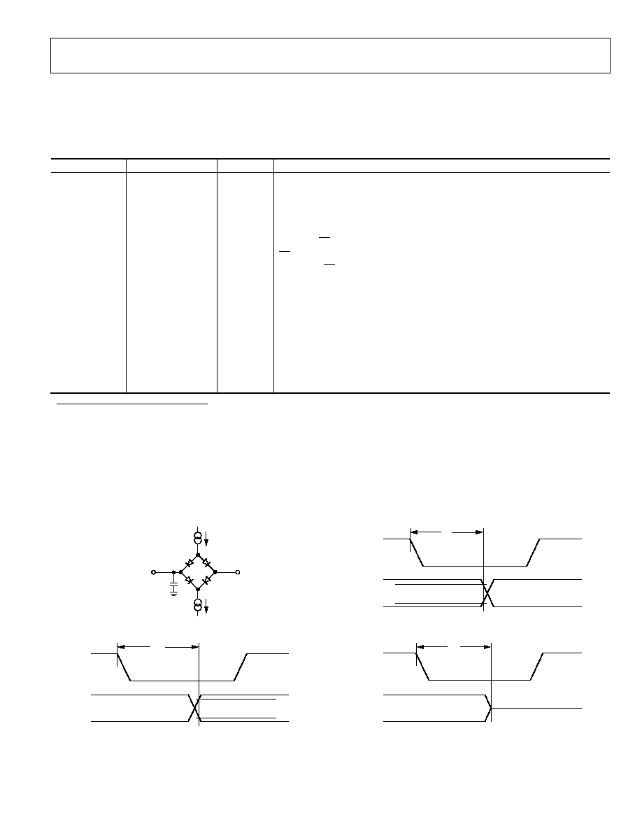
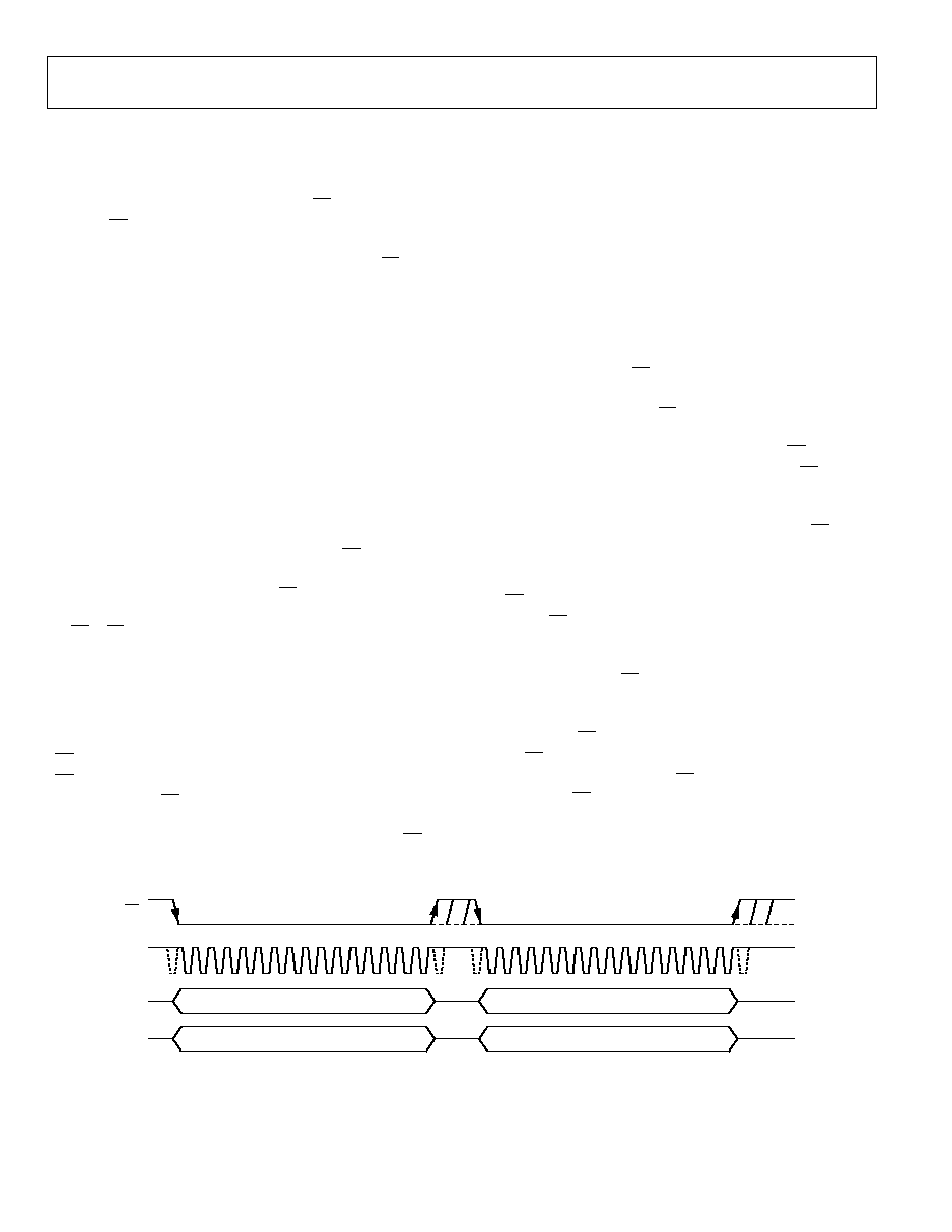
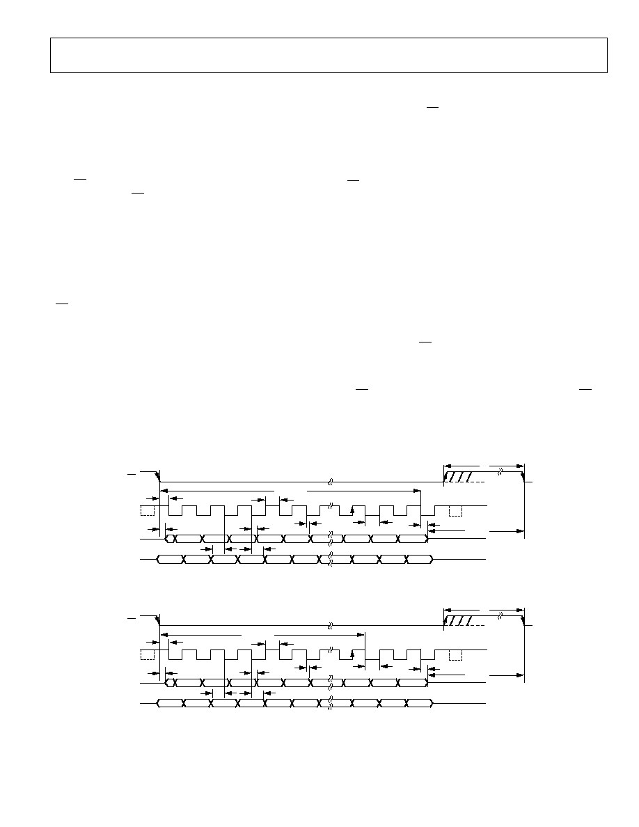
TIMING DIAGRAMS
04350-0-002
200
µ
A
I
OL
200
µ
A
I
OH
1.6V
TO OUTPUT
PIN
C
L
50pF
Figure 2. Load Circuit for Digital Output Timing Specifications
04350-0-003
SCLK
V
IH
V
IL
DOUT
t
4
Figure 3. Access Time after SCLK Falling Edge
04350-0-004
SCLK
V
IH
V
IL
DOUT
t
7
Figure 4. Hold Time after SCLK Falling Edge
04350-0-005
SCLK
1.6V
DOUT
t
10
Figure 5. SCLK Falling Edge to DOUT Three-State
AD7911/AD7921
Rev. 0 | Page 8 of 28
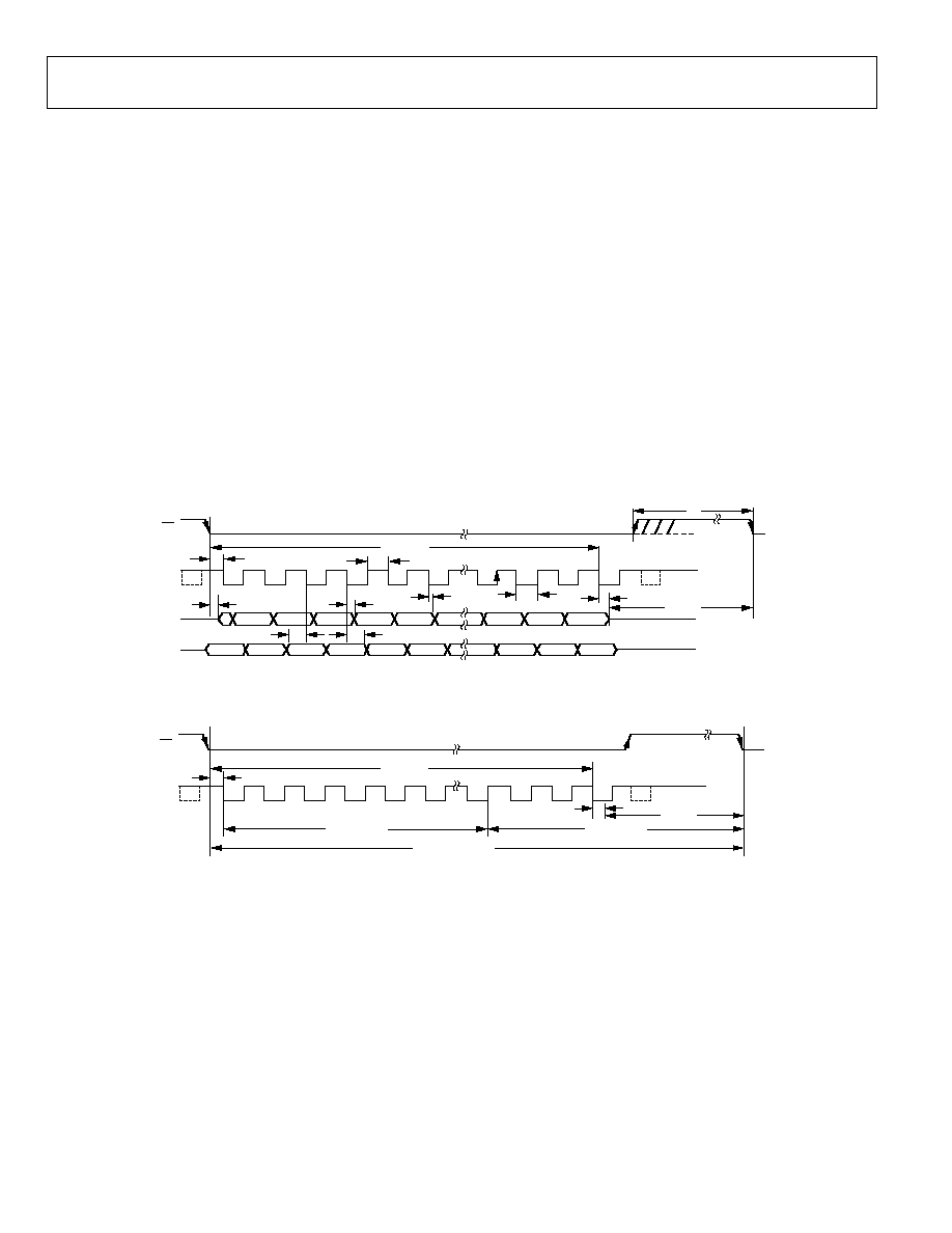
TIMING EXAMPLES
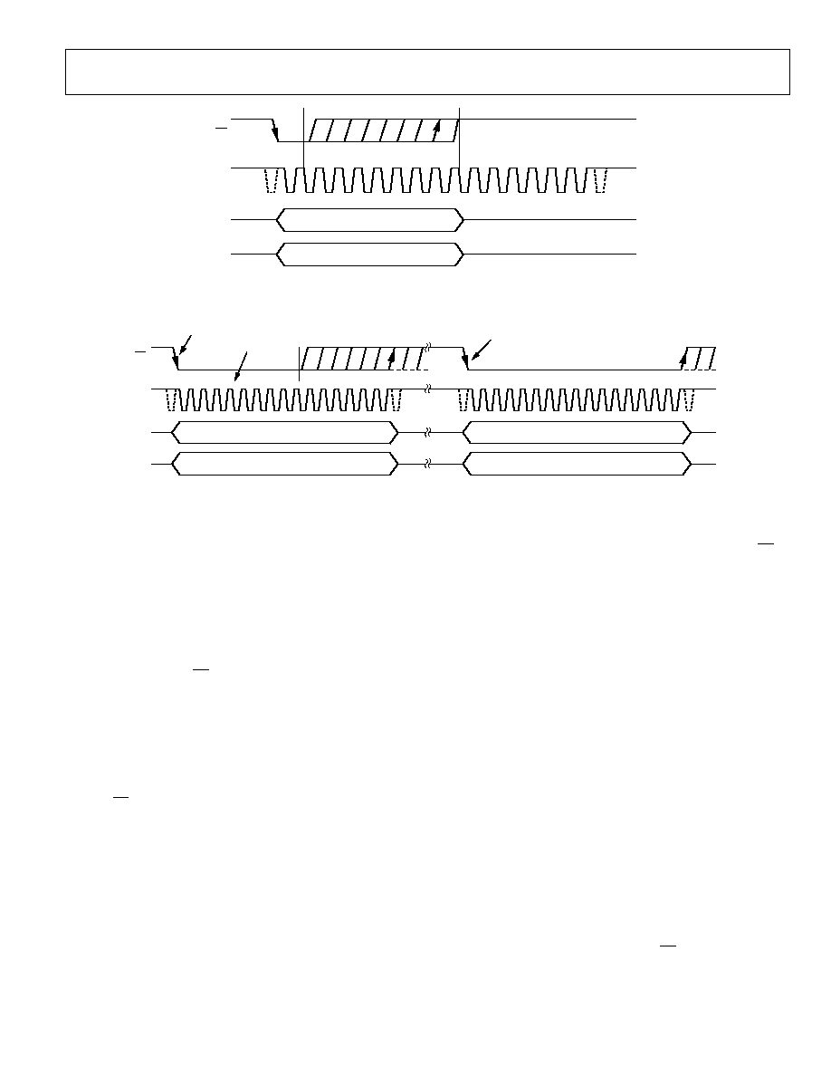
Figure 6 and Figure 7 show some of the timing parameters from
the Timing Specifications section.
Timing Example 1
As shown in Figure 7, when f
SCLK
= 5 MHz and the throughput is
250 kSPS, the cycle time is
t
2
+ 12.5(1/f
SCLK
) + t
ACQ
= 4 µs
With t
2
= 10 ns minimum, then t
ACQ
is 1.49 µs, which satisfies
the requirement of 290 ns for t
ACQ
.
In Figure 7, t
ACQ
is comprised of 2.5(1/f
SCLK
) + t
10
+ t
QUIET
, where
t
10
= 30 ns maximum. This allows a value of 960 ns for t
QUIET
,
satisfying the minimum requirement of 30 ns.
Timing Example 2
The AD7921 can also operate with slower clock frequencies. As
shown in Figure 7, when f
SCLK
= 2 MHz and the throughput rate
is 100 KSPS, the cycle time is
t
2
+ 12.5(1/f
SCLK
) + t
ACQ
= 10 µs
With t
2
= 10 ns minimum, then t
ACQ
is 3.74 µs, which satisfies
the requirement of 290 ns for t
ACQ
.
In Figure 7, t
ACQ
is comprised of 2.5(1/f
SCLK
) + t
10
+ t
QUIET
, where
t
10
= 30 ns maximum. This allows a value of 2.46 µs for t
QUIET
,
satisfying the minimum requirement of 30 ns.
In this example, as with other slower clock values, the signal
might already be acquired before the conversion is complete,
but it is still necessary to leave 30 ns minimum t
QUIET
between
conversions. In this example, the signal should be fully acquired
at approximately point C in Figure 7.
04350-0-006
ZERO
X
1
2
3
4
5
13
14
15
16
X
CHN
X
X
X
X
X
X
CHN
X
DB11
DB10
DB2
DB1
DB0
Z
t
2
t
6
t
4
t
8
t
9
t
3
t
7
t
5
t
10
t
1
t
QUIET
t
CONVERT
SCLK
CS
DOUT
THREE-STATE
THREE-STATE
DIN
B
Figure 6. AD7921 Serial Interface Timing Diagram
04350-0-007
1
2
3
4
5
13
14
15
16
t
QUIET
t
ACQUISITION
1/THROUGHPUT
12.5(1/f
SCLK
)
t
CONVERT
B
C
SCLK
CS
t
10
t
2
Figure 7. Serial Interface Timing Example
AD7911/AD7921
Rev. 0 | Page 9 of 28
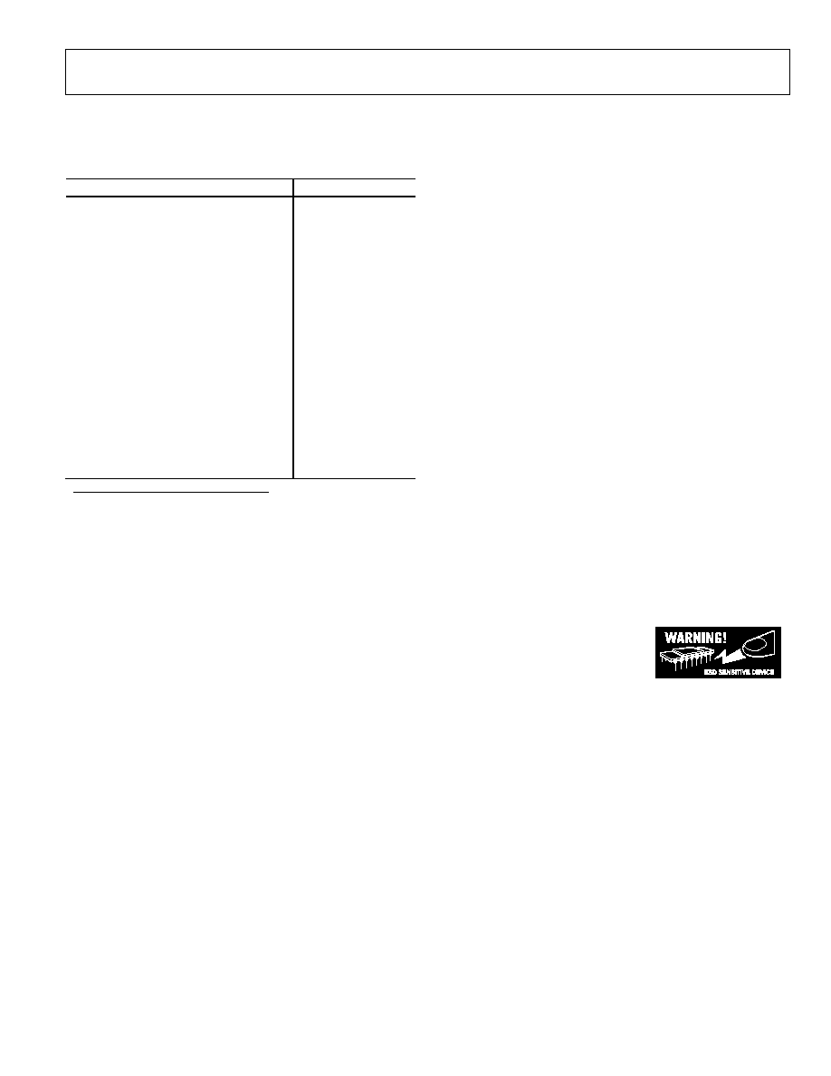
ABSOLUTE MAXIMUM RATINGS
T
A
= 25°C, unless otherwise noted.
Table 4.
Parameter Rating
V
DD
to GND
-0.3 V to +7 V
Analog Input Voltage to GND
-0.3 V to V
DD
+ 0.3 V
Digital Input Voltage to GND
-0.3 V to +7 V
Digital Output Voltage to GND
-0.3 V to V
DD
+ 0.3 V
Input Current to Any Pin except Supplies
1
±10 mA
Operating Temperature Range
Commercial (A Grade)
-40°C to +85°C
Storage Temperature Range
-65°C to +150°C
Junction Temperature
150°C
TSOT Package
JA
Thermal Impedance
207°C/W
MSOP Package
JA
Thermal Impedance
205.9°C/W
JC
Thermal Impedance
43.74°C/W
Lead Temperature Soldering
Reflow (10 s to 30 s)
235 (0/+5)°C
ESD 2
kV
1
Transient currents of up to 100 mA do not cause SCR latch-up.
Stresses above those listed under Absolute Maximum Ratings
may cause permanent damage to the device. This is a stress
rating only and functional operation of the device at these or
any other conditions above those indicated in the operational
section of this specification is not implied. Exposure to absolute
maximum rating conditions for extended periods may affect
device reliability.
ESD CAUTION
ESD (electrostatic discharge) sensitive device. Electrostatic charges as high as 4000 V readily accumulate on
the human body and test equipment and can discharge without detection. Although this product features
proprietary ESD protection circuitry, permanent damage may occur on devices subjected to high energy
electrostatic discharges. Therefore, proper ESD precautions are recommended to avoid performance
degradation or loss of functionality.
AD7911/AD7921
Rev. 0 | Page 10 of 28
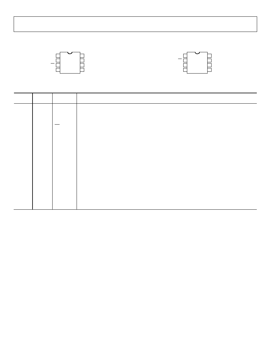
PIN CONFIGURATIONS AND FUNCTION DESCRIPTIONS
04350-0-008
V
IN1
V
IN0
GND
V
DD
8
7
6
5
DIN
1
SCLK
2
CS
3
DOUT
4
AD7911/
AD7921
8-LEAD TSOT
TOP VIEW
(Not to Scale)
Figure 8. 8-Lead TSOT Pin Configuration
04350-0-034
V
DD
GND
V
IN0
V
IN1
8
7
6
5
DOUT
1
CS
2
SCLK
3
DIN
4
AD7911/
AD7921
8-LEAD MSOP
TOP VIEW
(Not to Scale)
Figure 9. 8-Lead MSOP Pin Configuration
Table 5. Pin Function Descriptions
TSOT
Pin No.
MSOP
Pin No.
Mnemonic Function
1 4 DIN
Data In. Logic input. The channel to be converted is provided on this input and is clocked into an
internal register on the falling edge of SCLK.
2 3 SCLK
Serial Clock. Logic input. SCLK provides the serial clock for accessing data from the part. This clock
input is also used as the clock source for the AD7911/AD7921's conversion process.
3 2 CS
Chip Select. Active low logic input. This input provides the dual function of initiating conversions on
the AD7911/AD7921 and framing the serial data transfer.
4 1 DOUT
Data Out. Logic output. The conversion result from the AD7911/AD7921 is provided on this output as a
serial data stream. The bits are clocked out on the falling edge of the SCLK signal.
For the AD7921, the data stream consists of two leading zeros; the channel identifier bit, which
identifies the channel that the conversion result corresponds to; followed by an invalid bit that
matches up to the channel identifier bit; followed by the 12 bits of conversion data, with MSB first.
For the AD7911, the data stream consists of two leading zeros; the channel identifier bit, which
identifies the channel that the conversion result corresponds to; followed by an invalid bit that
matches up to the channel identifier bit; followed by the 10 bits of conversion data, with MSB first and
two trailing zeros.
5 8 V
DD
Power Supply Input. The V
DD
range for the AD7911/AD7921 is from 2.35 V to 5.25 V.
6 7 GND
Analog Ground. Ground reference point for all circuitry on the AD7911/AD7921. All analog input
signals should be referred to this GND voltage.
7, 8
6, 5
V
IN0
, V
IN1
Analog Inputs. These two single-ended analog input channels are multiplexed into the on-chip track-
and-hold amplifier. The analog input channel to be converted is selected by writing to the third MSB
on the DIN pin. The input range is 0 to V
DD
.

AD7911/AD7921
Rev. 0 | Page 11 of 28
TERMINOLOGY
Integral Nonlinearity
The maximum deviation from a straight line passing through
the endpoints of the ADC transfer function. For the AD7911/
AD7921, the endpoints of the transfer function are zero scale, a
point 1 LSB below the first code transition, and full scale, a
point 1 LSB above the last code transition.
Differential Nonlinearity
The difference between the measured and the ideal 1 LSB
change between any two adjacent codes in the ADC.
Offset Error
The deviation of the first code transition (00...000) to
(00...001) from the ideal, that is, AGND + 1 LSB.
Offset Error Match
The difference in offset error between any two channels.
Gain Error
The deviation of the last code transition (111...110) to
(111...111) from the ideal, that is, V
REF
- 1 LSB after the offset
error has been adjusted out.
Gain Error Match
The difference in gain error between any two channels.
Total Unadjusted Error
A comprehensive specification that includes gain error, linearity
error, and offset error.
Channel-to-Channel Isolation
A measure of the level of crosstalk between channels. It is
measured by applying a full-scale sine wave signal of 20 kHz to
500 kHz to the nonselected input channel and determining how
much that signal is attenuated in the selected channel with a
10 kHz signal. The figure is given worst case across both
channels for the AD7911/AD7921.
Track-and-Hold Acquisition Time
The time required for the output of the track-and-hold
amplifier to reach its final value within ±1 LSB after the end of
conversion. The track-and-hold amplifier returns to track mode
at the end of conversion. See the Serial Interface section for
more details.
Signal-to-Noise and Distortion Ratio (SINAD)
The measured ratio of signal-to-noise and distortion at the
output of the A/D converter. The signal is the rms value of the
sine wave, and noise is the rms sum of all nonfundamental
signals up to half the sampling frequency (fs/2), including
harmonics but excluding dc.
Signal-to-Noise Ratio (SNR)
The measured ratio of signal to noise at the output to the A/D
converter. The signal is the rms value of the sine wave input.
Noise is the rms quantization error within the Nyquist
bandwidth (fs/2). The rms value of a sine wave is one-half its
peak-to-peak value divided by 2, and the rms value for the
quantization noise is q/12. The ratio is dependent on the
number of quantization levels in the digitization process; the
more levels, the smaller the quantization noise. For an ideal
N-bit converter, the SNR is defined as
dB
76
1
02
6
.
N
.
SNR
+
=
Therefore, for a 12-bit converter, SNR is 74 dB; for a 10-bit
converter, SNR is 62 dB.
However, various error sources in the ADC cause the measured
SNR to be less than the theoretical value. These errors occur due
to integral and differential nonlinearities, internal ac noise
sources, and so on.
Total Harmonic Distortion (THD)
The ratio of the rms sum of harmonics to the fundamental,
which is defined as
1
2
6
2
5
2
4
2
2
2
V
V
V
V
V
V
THD
+
+
+
+
=
3
log
20
)
dB
(
where:
V
1
is the rms amplitude of the fundamental.
V
2
, V
3
, V
4
, V
5
, and V
6
are the rms amplitudes of the second
through the sixth harmonics.
Peak Harmonic or Spurious Noise
The ratio of the rms value of the next largest component in the
ADC output spectrum (up to fs/2 and excluding dc) to the rms
value of the fundamental. Normally, the value of this specifica-
tion is determined by the largest harmonic in the spectrum, but
for ADCs where the harmonics are buried in the noise floor, it is
a noise peak.

AD7911/AD7921
Rev. 0 | Page 12 of 28
Intermodulation Distortion
With inputs consisting of sine waves at two frequencies, fa and
fb, any active device with nonlinearities creates distortion
products at sum and difference frequencies of mfa ± nfb, where
m, n = 0, 1, 2, 3, and so on. Intermodulation distortion terms are
those for which neither m nor n is equal to zero. For example,
the second-order terms include (fa + fb) and (fa - fb), while the
third-order terms include (2fa + fb), (2fa - fb), (fa + 2fb), and
(fa - 2fb).
The AD7911/AD7921 are tested using the CCIF standard,
where two input frequencies are used (see fa and fb in the
Specifications section). In this case, the second-order terms are
usually distanced in frequency from the original sine waves,
while the third-order terms are usually at a frequency close to
the input frequencies. As a result, the second-order and third-
order terms are specified separately. The calculation of the
intermodulation distortion is as in the THD specification,
where it is defined as the ratio of the rms sum of the individual
distortion products to the rms amplitude of the sum of the
fundamentals expressed in dB.
AD7911/AD7921
Rev. 0 | Page 13 of 28
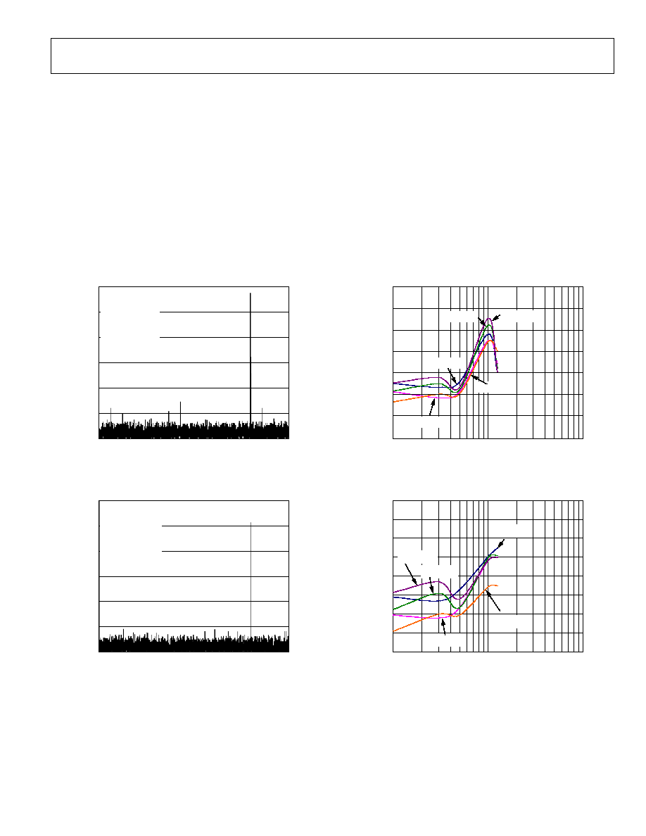
TYPICAL PERFORMANCE CHARACTERISTICS
Figure 10 and Figure 11 show typical FFT plots for the AD7921
and AD7911, respectively, at a 250 kSPS sample rate and
100 kHz input frequency.
Figure 12 shows the SINAD ratio performance versus the input
frequency for various supply voltages while sampling at
250 kSPS with a SCLK frequency of 5 MHz for the AD7921.
Figure 13 shows the SNR ratio performance versus the input
frequency for various supply voltages while sampling at
250 kSPS with an SCLK frequency of 5 MHz for the AD7921.
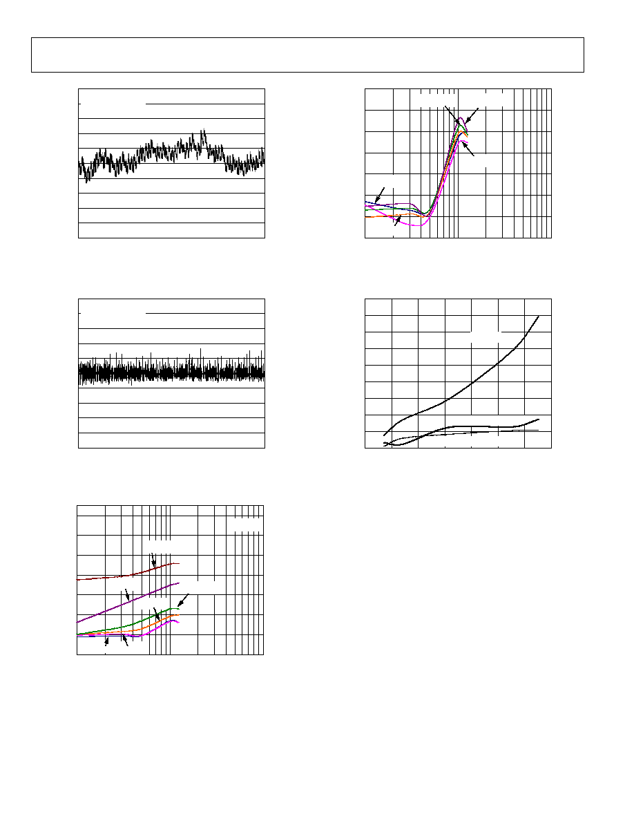
Figure 14 and Figure 15 show INL and DNL performance for
the AD7921.
Figure 16 shows a graph of the total harmonic distortion versus
the analog input frequency for different source impedances
when using a supply voltage of 3.6 V and a sampling rate of
250 kSPS. See the Analog Input section.
Figure 17 shows a graph of the total harmonic distortion versus
the analog input frequency for various supply voltages while
sampling at 250 kSPS with an SCLK frequency of 5 MHz.
Figure 18 shows the shutdown current versus the voltage supply
for different operating temperatures.
5
115
95
75
55
35
15
0
20
40
60
80
100
120
04350-0-009
FREQUENCY (kHz)
S
NR (dB)
8192 POINT FFT
V
DD
= 2.7V
F
SAMP
= 250kSPS
F
IN
= 100kHz
SNR = 73.13dB
SINAD = 72.73dB
THD = 83.30dB
SFDR = 86.15dB
Figure 10. AD7921 Dynamic Performance at 250 kSPS
8192 POINT FFT
V
DD
= 2.7V
F
SAMP
= 250kSPS
F
IN
= 100kHz
SNR = 73.13dB
SINAD = 72.73dB
THD = 83.30dB
SFDR = 86.15dB
5
115
95
75
55
35
15
0
20
40
60
80
100
120
04350-0-010
FREQUENCY (kHz)
S
NR (dB)
8192 POINT FFT
V
DD
= 2.7V
F
SAMP
= 250kSPS
F
IN
= 100kHz
SNR = 61.75dB
SINAD = 61.74dB
THD = 86.24dB
SFDR = 84.46dB
Figure 11. AD7911 Dynamic Performance at 250 kSPS
70.5
74.0
73.5
73.0
72.5
72.0
71.5
71.0
10
100
1k
04350-0-011
FREQUENCY (kHz)
S
I
NAD (dB)
V
DD
= 3.6V
V
DD
= 5.25V
V
DD
= 4.75V
V
DD
= 2.35V
V
DD
= 2.7V
Figure 12. AD7921 SINAD vs. Input Frequency at 250 kSPS
72.0
73.6
73.4
73.2
73.0
72.8
72.4
72.2
72.6
10
100
1k
04350-0-012
FREQUENCY (kHz)
S
NR (dB)
V
DD
= 2.35V
V
DD
= 3.6V
V
DD
= 5.25V
V
DD
= 4.75V
V
DD
= 2.7V
Figure 13. AD7921 SNR vs. Input Frequency at 250 kSPS
AD7911/AD7921
Rev. 0 | Page 14 of 28
1.0
1.0
0.8
0.6
0.4
0.2
0
0.2
0.4
0.6
0.8
0
4096
3584
3072
2560
2048
1536
1024
512
04350-0-013
CODE
INL E
R
ROR (LS
B
)
V
DD
= 2.7V
F
SAMP
= 250kSPS
TEMPERATURE = 25
°
C
Figure 14. AD7921 INL Performance
1.0
1.0
0.8
0.6
0.4
0.2
0
0.2
0.4
0.6
0.8
0
4096
3584
3072
2560
2048
1536
1024
512
04350-0-014
CODE
DNL E
R
ROR (LS
B
)
V
DD
= 2.7V
F
SAMP
= 250kSPS
TEMPERATURE = 25
°
C
Figure 15. AD7921 DNL Performance
95
85
75
65
55
35
25
45
10
100
1k
04350-0-015
FREQUENCY (kHz)
THD (dB)
R
IN
= 1k
R
IN
= 500
R
IN
= 100
R
IN
= 50
R
IN
= 10
R
IN
= 0
V
DD
= 3.6V
Figure 16. THD vs. Analog Input Frequency for Various Source Impedances
74
76
78
80
82
84
86
88
10
100
1k
04350-0-016
FREQUENCY (kHz)
THD (dB)
V
DD
= 2.35V
V
DD
= 3.6V
V
DD
= 5.25V
V
DD
= 4.75V
V
DD
= 2.7V
Figure 17. THD vs. Analog Input Frequency for Various Supply Voltages
180
160
0
20
40
60
80
100
120
140
2.0
5.5
5.0
4.5
4.0
3.5
3.0
2.5
04350-0-017
SUPPLY VOLTAGE (V)
S
HUTDOWN CURRE
NT (nA)
TEMPERATURE = +25
°
C
TEMPERATURE = +85
°
C
TEMPERATURE = 40
°
C
Figure 18. Shutdown Current vs. Supply Voltage
AD7911/AD7921
Rev. 0 | Page 15 of 28
CIRCUIT INFORMATION
The AD7911/AD7921 are fast, 2-channel, 10-/12-bit, single
supply, analog-to-digital converters (ADCs), respectively. The
parts can be operated from a 2.35 V to 5.25 V supply. When
operated from either a 5 V supply or a 3 V supply, the
AD7911/AD7921 are capable of throughput rates of 250 kSPS
when provided with a 5 MHz clock.
The AD7911/AD7921 provide the user with an on-chip track-
and-hold, an ADC, and a serial interface, all housed in a tiny 8-
lead TSOT package or an 8-lead MSOP package, which offer the
user considerable space-saving advantages over alternative
solutions. The serial clock input accesses data from the parts,
controls the transfer of data written to the ADC, and provides
the clock source for the successive approximation ADC. The
analog input range is 0 to V
DD
. An external reference is not
required for the ADC, and neither is there a reference on-chip.
The reference for the AD7911/AD7921 is derived from the
power supply and, therefore, gives the widest dynamic input
range.
The AD7911/AD7921 feature a power-down option that allows
power saving between conversions. The power-down feature is
implemented across the standard serial interface as described in
the Modes of Operation section.
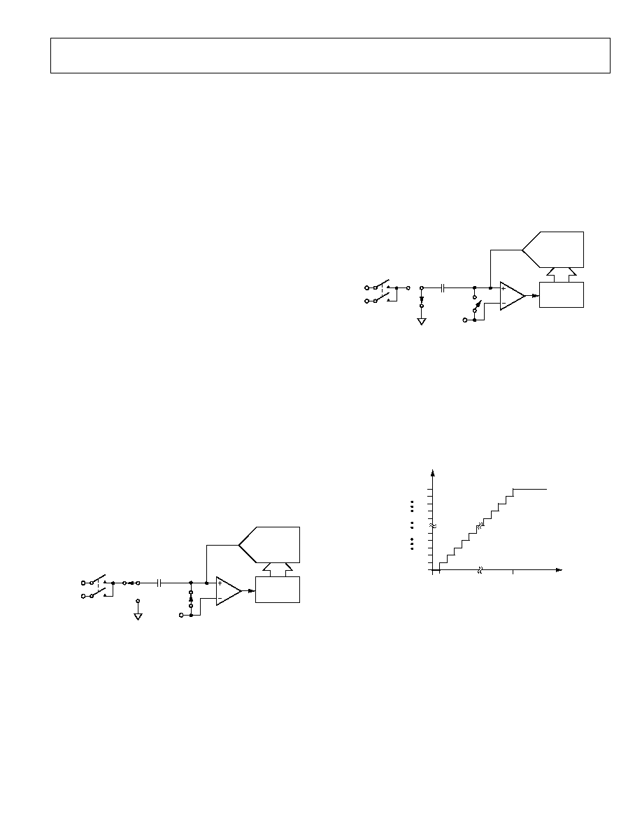
CONVERTER OPERATION
The AD7911/AD7921 are 10-/12-bit successive approximation
ADCs based around a charge redistribution DAC. Figure 19 and
Figure 20 show simplified schematics of the ADC. Figure 19
shows the ADC during its acquisition phase. SW2 is closed and
SW1 is in Position A, the comparator is held in a balanced
condition, and the sampling capacitor acquires the signal on the
selected V
IN
channel.
04350-0-018
COMPARATOR
ACQUISITION
PHASE
V
DD
/2
SW2
SW1
V
IN0
V
IN1
SAMPLING
CAPACITOR
AGND
A
B
CHARGE
REDISTRIBUTION
DAC
CONTROL
LOGIC
Figure 19. ADC Acquisition Phase
When the ADC starts a conversion (see Figure 20), SW2 opens
and SW1 moves to Position B, causing the comparator to
become unbalanced. The control logic and the charge
redistribution DAC are used to add and subtract fixed amounts
of charge from the sampling capacitor to bring the comparator
back into a balanced condition. When the comparator is
rebalanced, the conversion is complete. The control logic
generates the ADC output code. Figure 21 shows the ADC
transfer function.
04350-0-019
COMPARATOR
CONVERSION
PHASE
V
DD
/2
SW2
SW1
V
IN0
V
IN1
SAMPLING
CAPACITOR
AGND
A
B
CHARGE
REDISTRIBUTION
DAC
CONTROL
LOGIC
Figure 20. ADC Conversion Phase
ADC TRANSFER FUNCTION
The output coding of the AD7911/AD7921 is straight binary.
The designed code transitions occur at the successive integer
LSB values, that is, 1 LSB, 2 LSB, and so on. The LSB size is
V
DD
/4096 for the AD7921 and V
DD
/1024 for the AD7911. The
ideal transfer characteristic for the AD7911/AD7921 is shown
in Figure 21.
04350-0-020
000...000
0V
ADC CODE
ANALOG INPUT
111...111
000...001
111...000
011...111
111...110
000...010
1LSB = V
DD
/4096 (AD7921)
1LSB = V
DD
/1024 (AD7911)
+V
DD
1LSB
1LSB
Figure 21. AD7911/AD7921 Transfer Characteristic
AD7911/AD7921
Rev. 0 | Page 16 of 28
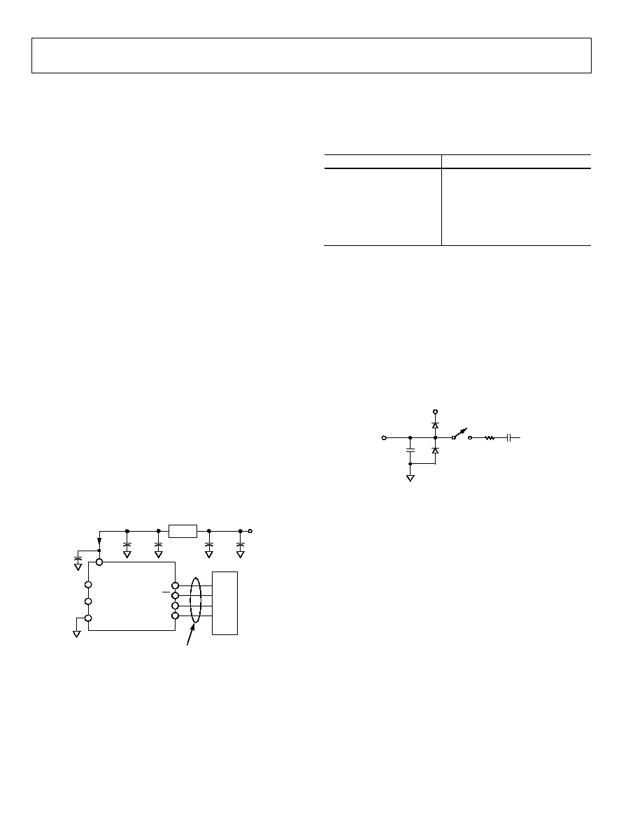
TYPICAL CONNECTION DIAGRAM
Figure 22 shows a typical connection diagram for the AD7911/
AD7921. V
REF
is taken internally from V
DD
and as such V
DD
should be well decoupled. This provides an analog input range
of 0 V to V
DD
. The conversion result is output in a 16-bit word
with two leading zeros, followed by the channel identifier bit
that identifies the channel converted, followed by an invalid bit
that matches up to the channel converted, followed by the MSB
of the 12-bit or 10-bit result. For the AD7911, the 10-bit result is
followed by two trailing zeros. See the Serial Interface section.
Alternatively, because the supply current required by the
AD7911/AD7921 is so low, a precision reference can be used as
the supply source to the AD7911/AD7921. A REF19x voltage
reference (REF195 for 5 V or REF193 for 3 V) can be used to
supply the required voltage to the ADC (see Figure 22). This
configuration is especially useful, if the power supply is quite
noisy or if the system supply voltages are at some value other
than 5 V or 3 V (for example, 15 V). The REF19x outputs a
steady voltage to the AD7911/AD7921. If the low dropout
REF193 is used, the current it needs to supply to the AD7911/
AD7921 is typically 1.5 mA. When the ADC is converting at a
rate of 250 kSPS, the REF193 needs to supply a maximum of
2 mA to the AD7911/AD7921. The load regulation of the
REF193 is typically 10 ppm/mA (REF193, V
S
= 5 V), which
results in an error of 20 ppm (60 µV) for the 2 mA drawn from
it. This corresponds to a 0.082 LSB error for the AD7921 with
V
DD
= 3 V from the REF193 and a 0.061 LSB error for the
AD7911.
For applications where power consumption is a concern, the
power-down mode of the ADC and the sleep mode of the
REF19x reference should be used to improve power perform-
ance. See the Modes of Operation section.
04350-0-021
AD7911/
AD7921
V
DD
V
IN0
SERIAL
INTERFACE
0V TO V
DD
INPUT
µ
C/
µ
P
V
IN1
GND
SCLK
CS
DIN
DOUT
0.1
µ
F
10
µ
F
1
µ
F
TANT
0.1
µ
F
680nF
3V
5V
SUPPLY
1.5mA
REF193
Figure 22. REF193 as Power Supply to AD7911/AD7921
Table 6 provides some typical performance data with various
references used as a V
DD
source and a 50 kHz input tone under
the same setup conditions.
Table 6. AD7921 Performance for Various Voltage
References IC
Reference Tied to V
DD
AD7921 SNR Performance (dB)
AD780 at 3 V
-73
REF193 -72.42
ADR433 -72.9
AD780 at 2.5 V
-72.86
REF192 -72.27
ADR421 -72.75
ANALOG INPUT
Figure 23 shows an equivalent circuit of the analog input
structure of the AD7911/AD7921. The two diodes, D1 and D2,
provide ESD protection for the analog input. Care must be
taken to ensure that the analog input signal never exceeds the
supply rails by more than 300 mV, because this would cause
these diodes to become forward biased and start conducting
current into the substrate. The maximum current these diodes
can conduct without causing irreversible damage to the part is
10 mA.
04350-0-022
C1
6pF
C2
20pF
R1
D1
D2
CONVERSION PHASE--SWITCH OPEN
TRACK PHASE--SWITCH CLOSED
V
DD
V
IN
Figure 23. Equivalent Analog Input Circuit
The capacitor C1 in Figure 23 is typically about 6 pF and can
primarily be attributed to pin capacitance. The resistor R1 is a
lumped component made up of the on resistance of a track-
and-hold switch and also includes the on resistance of the input
multiplexer. This resistor is typically about 100 . The capacitor
C2 is the ADC sampling capacitor and has a capacitance of
20 pF typically.
For ac applications, removing high frequency components from
the analog input signal is recommended using a band-pass filter
on the relevant analog input pin. In applications where
harmonic distortion and signal-to-noise ratio are critical, the
analog input should be driven from a low impedance source.
Large source impedances can significantly affect the ac
performance of the ADC. This might necessitate the use of an
input buffer amplifier. The choice of the op amp is a function of
the particular application.
AD7911/AD7921
Rev. 0 | Page 17 of 28
Table 7 provides some typical performance data with various
op amps used as the input buffer, and a 50 kHz input tone under
the same setup conditions.
Table 7. AD7921 Performance for Various Input Buffers
Op Amp in the Input
Buffer
AD7921 SNR Performance (dB)
50 kHz Input , V
DD
= 3.6 V
Single op amps
AD8038
-72.79
AD8510
-72.35
AD8021
-72.2
Dual op amps
AD712
-72.68
AD8022
-72.88
When no amplifier is used to drive the analog input, the source
impedance should be limited to low values. The maximum
source impedance depends on the amount of total harmonic
distortion (THD) that can be tolerated. The THD increases as
the source impedance increases and performance degrades (see
Figure 16).
DIGITAL INPUTS
The digital inputs applied to the AD7911/AD7921 are not
limited by the maximum ratings that limit the analog input.
Instead, the digital inputs applied can go to 7 V and are not
restricted by the V
DD
+ 0.3 V limit as on the analog input. For
example, if the AD7911/AD7921 are operated with a V
DD
of 3 V,
then 5 V logic levels could be used on the digital inputs. How-
ever, it is important to note that the data output on DOUT still
has 3 V logic levels when V
DD
= 3 V. Another advantage of
SCLK, DIN, and CS not being restricted by the V
DD
+ 0.3 V limit
is that power supply sequencing issues are avoided. If CS, DIN,
or SCLK are applied before V
DD
, then there is no risk of latch-up
as there would be on the analog inputs, if a signal greater than
0.3 V were applied prior to V
DD
.
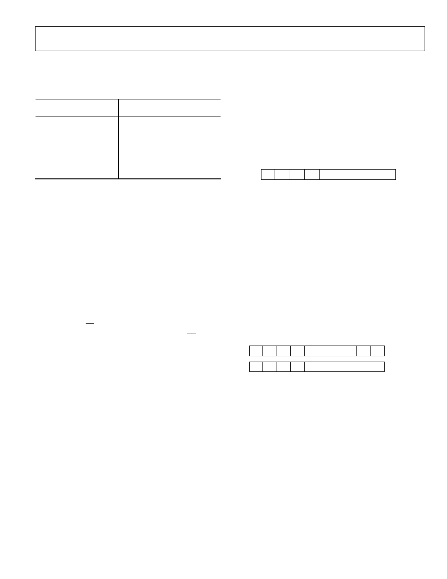
DIN INPUT
The channel to be converted on in the next conversion is
selected by writing to the DIN pin. Data on the DIN pin is
loaded into the AD7911/AD7921 on the falling edge of SCLK.
The data is transferred into the part on the DIN pin at the same
time that the conversion result is read from the part.
Only the third bit of the DIN word is used; the rest are ignored
by the ADC. The third MSB is the channel identifier bit, which
identifies the channel to be converted on in the next conversion,
V
IN0
(CHN = 0) or V
IN1
(CHN = 1).
04350-0-023
LSB
MSB
X
X
CHN
X
DON'T CARE
Figure 24. AD7911/AD7921 DIN Word
DOUT OUTPUT
The conversion result from the AD7911/AD7921 is provided on
this output as a serial data stream. The bits are clocked out on
the SCLK falling edge at the same time that the conversion is
taking place.
The serial data stream for the AD7921 consists of two leading
zeros followed by the bit that identifies the channel converted,
an invalid bit that matches up to the channel identifier bit, and
the 12-bit conversion result with MSB provided first.
For the AD7911, the serial data stream consists of two leading
zeros followed by the bit that identifies the channel converted,
an invalid bit that matches up to the channel identifier bit, and
the 10-bit conversion result with MSB provided first, followed
by two trailing zeros.
04350-0-024
LSB
AD7911
MSB
0
0
0
0
CHN
X
CONVERSION RESULT
AD7921
0
0
CHN
X
CONVERSION RESULT
Figure 25. AD7911/AD7921 DOUT Word
AD7911/AD7921
Rev. 0 | Page 18 of 28
MODES OF OPERATION
The two modes of operation of the AD7911/AD7921 are
normal mode and power-down mode. The mode of operation is
selected by controlling the logic state of the CS signal. The point
at which CS is pulled high after the conversion has been initi-
ated determines whether the AD7911/AD7921 enter power-
down mode. Similarly, if already in power-down mode, CS can
control whether the device returns to normal operation or
remains in power-down mode.
Power-down mode is designed to provide flexible power
management options and to optimize the ratio of power
dissipation to throughput rate for different application
requirements.
NORMAL MODE
Normal mode is intended for the fastest throughput rate
performance. The user does not have to worry about any
power-up time, because the AD7911/AD7921 remain fully
powered all the time. Figure 26 shows the operation of the
AD7911/AD7921 in this mode.
The conversion is initiated on the falling edge of CS, as
described in the Serial Interface section. To ensure that the part
remains fully powered up at all times, CS must remain low until
at least 10 SCLK falling edges have elapsed after the falling edge
of CS. If CS is brought high any time after the 10th SCLK falling
edge but before the end of t
CONVERT
, the part remains powered-
up, but the conversion is terminated and DOUT goes back into
three-state. For the AD7911/AD7921, a minimum of 14 and
16 serial clock cycles, respectively, are needed to complete the
conversion and access the complete conversion result.
CS can idle high until the next conversion or can idle low until
CS returns high sometime prior to the next conversion
(effectively idling CS low). Once a data transfer is complete
(DOUT has returned to three-state), another conversion can be
initiated after the quiet time, t
QUIET
, has elapsed by bringing CS
low again.
POWER-DOWN MODE
Power-down mode is intended for use in applications where
slower throughput rates are required. Either the ADC is
powered down between each conversion, or a series of
conversions can be performed at a high throughput rate and
then the ADC is powered down for a relatively long duration
between these bursts of several conversions. When the
AD7911/AD7921 are in power-down mode, all analog circuitry
is powered down.
To enter power-down mode, the conversion process must be
interrupted by bringing CS high any time after the second
falling edge of SCLK and before the 10th falling edge of SCLK,
as shown in Figure 27. Once CS has been brought high in this
window of SCLKs, then the part enters power-down mode, the
conversion that was initiated by the falling edge of CS is
terminated, and DOUT goes back into three-state. If CS is
brought high before the second SCLK falling edge, then the part
remains in normal mode and does not power down. This helps
to avoid accidental power-down due to glitches on the CS line.
To exit this mode of operation and power the AD7911/AD7921
up again, a dummy conversion is performed. On the falling edge
of CS, the device begins to power up and continues to power up
as long as CS is held low until after the falling edge of the 10th
SCLK. The device is fully powered up once 16 SCLKs have
elapsed and valid data results from the next conversion, as
shown in Figure 28. If CS is brought high before the 10th falling
edge of SCLK, then the AD7911/AD7921 go back into power-
down mode. This helps to avoid accidental power-up due to
glitches on the CS line or an inadvertent burst of 8 SCLK cycles
while CS is low. Therefore, although the device might begin to
power up on the falling edge of CS, it powers down again on the
rising edge of CS, as long as this occurs before the 10th SCLK
falling edge.
04350-0-025
CS
1
10
12
14
16
1
10
12
14
16
AD7911/AD7921
SCLK
DIN
DOUT
CHANNEL FOR NEXT CONVERSION
CHANNEL FOR NEXT CONVERSION
CONVERSION RESULT
CONVERSION RESULT
Figure 26. Normal Mode Operation
AD7911/AD7921
Rev. 0 | Page 19 of 28
04350-0-026
INVALID DATA
THREE-STATE
INVALID DATA
THREE-STATE
1
CS
SCLK
DIN
DOUT
2
10
16
Figure 27. Entering Power- Down Mode
04350-0-027
1
10
THE PART BEGINS
TO POWER UP
THE PART GOES
INTO TRACK
THE PART IS FULLY
POWERED UP WITH V
IN
FULLY ACQUIRED
5
A
16
1
16
SCLK
CS
DIN
CHANNEL FOR NEXT CONVERSION
CHANNEL FOR NEXT CONVERSION
DOUT
INVALID DATA
CONVERSION RESULT
Figure 28. Exiting Power-Down Mode
POWER-UP TIME
The power-up time of the AD7911/AD7921 is 1 µs, which
means that with any frequency of SCLK up to 5 MHz, one
dummy cycle is always sufficient to allow the device to power
up. Once the dummy cycle is complete, the ADC is fully
powered up and the input signal is acquired properly. The quiet
time, t
QUIET
, must still be allowed from the point at which the
bus goes back into three-state after the dummy conversion to
the next falling edge of CS. When running at a 250 kSPS
throughput rate, the AD7911/AD7921 power up and acquire a
signal within ±1 LSB in one dummy cycle.
When powering up from power-down mode with a dummy
cycle, as in Figure 28, the track-and-hold that was in hold mode
while the part was powered down returns to track mode on the
fifth SCLK falling edge that the part receives after the falling
edge of CS. This is shown as point A in Figure 28. At this point,
the part starts to acquire the signal on the channel selected in
the current dummy conversion.
Although at any SCLK frequency one dummy cycle is sufficient
to power up the device and acquire V
IN
, it does not necessarily
mean that a full dummy cycle of 16 SCLKs must always elapse
to power up the device and acquire V
IN
fully. 1µs is sufficient to
power up the device and acquire the input signal. For example,
if a 5 MHz SCLK frequency was applied to the ADC, the cycle
time would be 3.2 µs. In one dummy cycle, 3.2 µs, the part
would be powered up and V
IN
acquired fully. However, after 1 µs
with a 5 MHz SCLK, only 5 SCLK cycles would have elapsed. At
this stage, the ADC would be fully powered up. In this case, CS
can be brought high after the 10th SCLK falling edge and
brought low again after a time, t
QUIET
, to initiate the conversion.
When power supplies are first applied to the AD7911/AD7921,
the ADC can power up in either power-down mode or normal
mode. Because of this, it is best to allow a dummy cycle to
elapse to ensure that the part is fully powered up before
attempting a valid conversion. Likewise, if the user wants to
keep the part in power-down mode while not in use and to
power up in power-down mode, then the dummy cycle can be
used to ensure that the device is in power-down mode by
executing a cycle such as that shown in Figure 27.
Once supplies are applied to the AD7911/AD7921, the power-
up time is the same as when powering up from the power-down
mode. It takes the part approximately 1 µs to power up fully in
normal mode. It is not necessary to wait 1 µs before executing a
dummy cycle to ensure the desired mode of operation. Instead,
the dummy cycle can occur directly after power is supplied to
the ADC. If the first valid conversion is then performed directly
after the dummy conversion, care must be taken to ensure that
adequate acquisition time has been allowed. When the ADC
powers up initially after supplies are applied, the track-and-hold
is in hold. It returns to track on the fifth SCLK falling edge that
the part receives after the falling edge of CS.
AD7911/AD7921
Rev. 0 | Page 20 of 28
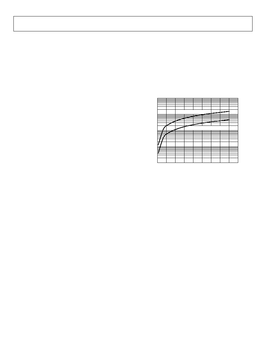
POWER VS. THROUGHPUT RATE
By using the power-down mode on the AD7911/AD7921 when
not converting, the average power consumption of the ADC
decreases at lower throughput rates. Figure 29 shows how, as the
throughput rate is reduced, the device remains in its power-
down state longer and the average power consumption over
time drops accordingly.
For example, if the AD7911/AD7921 are operating in a
continuous sampling mode with a throughput rate of 50 kSPS
and a SCLK of 5 MHz (V
DD
= 5 V) and the devices are placed in
power-down mode between conversions, then the power
consumption is calculated as follows. The power dissipation
during normal operation is 20 mW (V
DD
= 5 V). If one dummy
cycle powers up the part between conversions (3.2 µs), and the
remaining conversion time is another cycle (3.2 µs), then the
AD7911/AD7921 dissipate 20 mW for 6.4 µs during each
conversion cycle. If the throughput rate is 50 kSPS and the cycle
time is 20 µs, then the average power dissipated during each
cycle is
(6.4/20) × (20 mW) = 6.4 mW
If V
DD
= 3 V, SCLK= 5 MHz, and the device is again in power-
down mode between conversions, then the power dissipation
during normal operation is 6 mW. The AD7911/AD7921 now
dissipate 6 mW for 6.4 µs during each conversion cycle. With a
throughput rate of 50 kSPS, the average power dissipated during
each cycle is
(6.4/20) × (6 mW) = 1.92 mW
In the previous examples, the power dissipation when the part is
in power-down mode has not been taken into account, because
the shutdown current is so low that it does not have any effect
on the overall power dissipation value. Figure 29 shows the
power consumption versus throughput rate when using the
power-down mode between conversions with both 5 V and 3 V
supplies.
Power-down mode is intended for use with throughput rates of
approximately 120 kSPS and under, because higher sampling
rates do not have a power saving in power-down mode.
0.01
100
10
1
0.1
0
135
120
105
90
75
60
45
30
15
04350-0-035
THROUGHPUT (kSPS)
P
O
WE
R (mW)
V
DD
= 5V, SCLK = 5MHz
V
DD
= 3V, SCLK = 5MHz
Figure 29. Power Consumption vs. Throughput Rate
AD7911/AD7921
Rev. 0 | Page 21 of 28
SERIAL INTERFACE
Figure 30 and Figure 31 show the detailed timing diagrams for
serial interfacing to the AD7921 and AD7911, respectively. The
serial clock provides the conversion clock and also controls the
transfer of information from the AD7911/AD7921 during
conversion.
The CS signal initiates the data transfer and conversion process.
The falling edge of CS puts the track-and-hold into hold mode,
takes the bus out of three-state, the analog input is sampled at
this point, and the conversion is initiated.
For the AD7921, the conversion requires 16 SCLK cycles to
complete. Once 13 SCLK falling edges have elapsed, the track-
and-hold goes back into track on the next SCLK rising edge, as
shown in Figure 30 at Point B. On the 16th SCLK falling edge,
the DOUT line goes back into three-state. If the rising edge of
CS occurs before 16 SCLKs have elapsed, then the conversion is
terminated and the DOUT line goes back into three-state.
Otherwise, DOUT returns to three-state on the 16th SCLK
falling edge, as shown in Figure 30. Sixteen serial clock cycles
are required to perform the conversion process and to access
data from the AD7921.
For the AD7911, the conversion requires 14 SCLK cycles to
complete. Once 13 SCLK falling edges have elapsed, the track-
and-hold goes back into track on the next SCLK rising edge, as
shown in Figure 31 at Point B.
If the rising edge of CS occurs before 14 SCLKs have elapsed,
then the conversion is terminated and the DOUT line goes back
into three-state. If 16 SCLKs are considered in the cycle, DOUT
returns to three-state on the 16th SCLK falling edge, as shown
in Figure 31.
CS going low clocks out the first leading zero to be read in by
the microcontroller or DSP. The remaining data is then clocked
out by subsequent SCLK falling edges beginning with the
second leading zero. Therefore, the first falling clock edge on
the serial clock has the first leading zero provided and also
clocks out the second leading zero. The final bit in the data
transfer is valid on the 16th falling edge, having been clocked
out on the previous (15th) falling edge.
In applications with a slower SCLK, it is possible to read in data
on each SCLK rising edge. In that case, the first falling edge of
SCLK clocks out the second leading zero and it can be read in
the first rising edge. However, the first leading zero that is
clocked out when CS goes low is missed, unless it is not read in
the first falling edge. The 15th falling edge of SCLK clocks out
the last bit and it can be read in the 15th rising SCLK edge.
If CS goes low just after the SCLK falling edge has elapsed, CS
clocks out the first leading zero as before and it can be read in
the SCLK rising edge. The next SCLK falling edge clocks out
the second leading zero and it can be read in the following
rising edge.
04350-0-029
ZERO
X
1
2
3
4
5
13
14
15
16
X
CHN
X
X
X
X
X
X
CHN
X
DB11
DB10
DB2
DB1
DB0
Z
t
2
t
6
t
4
t
8
t
9
t
3
t
7
t
5
t
10
t
1
t
QUIET
t
CONVERT
SCLK
CS
DOUT
THREE-STATE
THREE-STATE
DIN
B
Figure 30. AD7921 Serial Interface Timing Diagram
04350-0-030
ZERO
X
1
2
3
4
5
13
14
15
16
X
CHN
X
X
X
X
X
X
CHN
X
DB9
DB8
DB0
ZERO
ZERO
Z
t
2
t
6
t
4
t
8
t
9
t
3
t
7
t
5
t
10
t
1
t
QUIET
t
CONVERT
SCLK
CS
DOUT
THREE-STATE
THREE-STATE
TWO TRAILING ZEROS
DIN
B
Figure 31. AD7911 Serial Interface Timing Diagram
AD7911/AD7921
Rev. 0 | Page 22 of 28
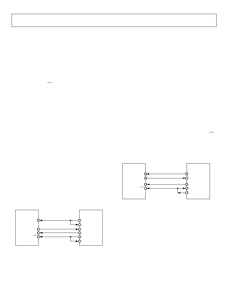
MICROPROCESSOR INTERFACING
The serial interface on the AD7911/AD7921 allows the parts to
be directly connected to a range of microprocessors. This
section explains how to interface the AD7911/AD7921 with
some of the more common microcontroller and DSP serial
interface protocols.
AD7911/AD7921 to TMS320C541 Interface
The serial interface on the TMS320C541 uses a continuous
serial clock and frame synchronization signals to synchronize
the data transfer operations with peripheral devices like the
AD7911/AD7921. The CS input allows easy interfacing between
the TMS320C541 and the AD7911/AD7921 without any glue
logic required. The serial port of the TMS320C541 is set up to
operate in burst mode (FSM = 1 in the serial port control
register, SPC) with the internal serial clock CLKX (MCM = 1 in
the SPC register) and the internal frame signal (TXM = 1 in the
SPC register); therefore, both pins are configured as outputs. For
the AD7921, the word length should be set to 16 bits (FO = 0 in
the SPC register). This DSP allows frames with a word length of
16 bits or 8 bits only. In the AD7911, therefore, where 14 bits are
required, the FO bit should be set up to 16 bits, and 16 SCLKs
are needed. For the AD7911, two trailing zeros are clocked out
in the last two clock cycles.
The values in the SPC register are as follows:
FO = 0
FSM = 1
MCM = 1
TXM = 1
To implement the power-down mode on the AD7911/AD7921,
the format bit, FO, can be set to 1, which sets the word length to
8 bits.
The connection diagram is shown in Figure 32. Note that, for
signal processing applications, the frame synchronization signal
from the TMS320C541 must provide equidistant sampling.
AD7911/
AD7921*
TMS320C541*
CLKX
DR
FSX
FSR
SCLK
DOUT
CS
CLKR
DX
DIN
04350-0-031
*ADDITIONAL PINS OMITTED FOR CLARITY
Figure 32. Interfacing to the TMS320C541
AD7911/AD7921 to ADSP-218x
The ADSP-218x family of DSPs are interfaced directly to the
AD7911/AD7921 without any glue logic required. The SPORT
control register should be set up as follows:
TFSW = RFSW = 1, alternate framing
INVRFS = INVTFS = 1, active low frame signal
DTYPE = 00, right-justify data
ISCLK = 1, internal serial clock
TFSR = RFSR = 1, frame every word
IRFS = 0, set up RFS as an input
ITFS = 1, set up TFS as an output
SLEN = 1111, 16 bits for the AD7921
SLEN = 1101, 14 bits for the AD7911
To implement the power-down mode, SLEN should be set to
0111 to issue an 8-bit SCLK burst. The connection diagram is
shown in Figure 33. The ADSP-218x has the TFS and RFS of the
SPORT tied together, with TFS set as an output and RFS set as
an input. The DSP operates in alternate framing mode and the
SPORT control register is set up as described previously. The
frame synchronization signal generated on the TFS is tied to CS
and, as with all signal processing applications, equidistant
sampling is necessary. However, in this example, the timer
interrupt is used to control the sampling rate of the ADC and,
under certain conditions, equidistant sampling might not be
achieved.
AD7911/
AD7921*
ADSP-218x*
SCLK
RFS
TFS
SCLK
CS
DR
DOUT
DT
DIN
04350-0-032
*ADDITIONAL PINS OMITTED FOR CLARITY
Figure 33. Interfacing to the ADSP-218x
The timer registers are loaded with a value that provides an
interrupt at the required sample interval. When an interrupt is
received, a value is transmitted with TFS/DT (ADC control
word). The TFS is used to control the RFS and, therefore, the
reading of data. The frequency of the serial clock is set in the
SCLKDIV register. When the instruction to transmit with TFS
is given, that is, TX0 = AX0, the state of the SCLK is checked.
The DSP waits until the SCLK has gone high, low, and high
again before transmission starts. If the timer and SCLK values
are chosen such that the instruction to transmit occurs on or
near the rising edge of SCLK, the data might be transmitted, or
it might wait until the next clock edge.
AD7911/AD7921
Rev. 0 | Page 23 of 28
For example, the ADSP-2189 has a master clock frequency of
40 MHz. If the SCLKDIV register is loaded with the value of 3,
then an SCLK of 5 MHz is obtained, and eight master clock
periods elapse for every one SCLK period. Depending on the
throughput rate selected, if the timer register is loaded with the
value 803 (803 + 1 = 804), then 100.5 SCLK occur between
interrupts and subsequently between transmit instructions. This
situation results in nonequidistant sampling, because the
transmit instruction occurs on a SCLK edge. If the number of
SCLKs between interrupts is a whole integer figure of N, then
equidistant sampling is implemented by the DSP.
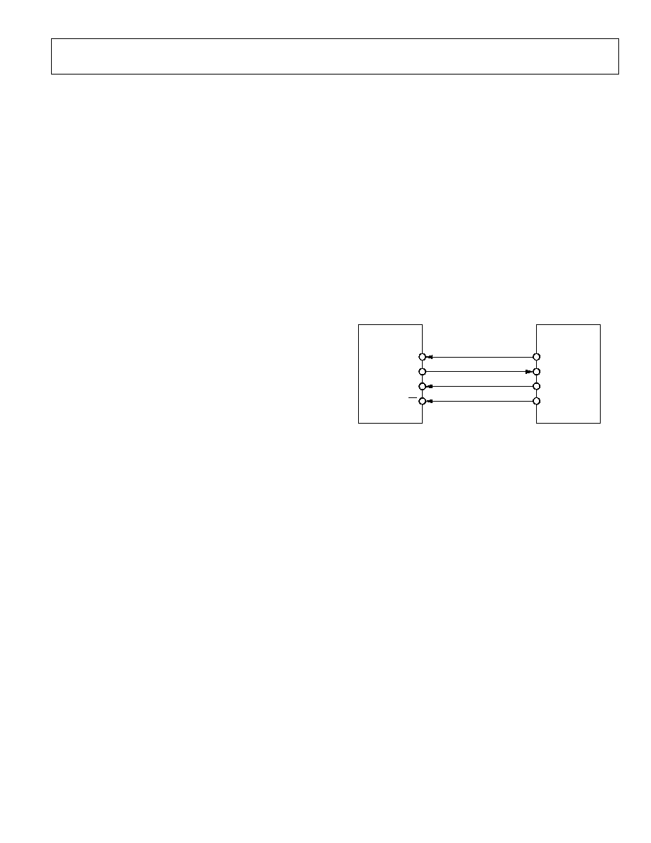
AD7911/AD7921 to DSP563xx Interface
The connection diagram in Figure 34 shows how the AD7911/
AD7921 can be connected to the SSI (synchronous serial
interface) of the DSP563xx family of DSPs from Motorola. The
SSI is operated in synchronous and normal mode (SYN = 1 and
MOD = 0 in the Control Register B, CRB) with internally
generated word frame sync for both Tx and Rx (Bits FSL1 = 0
and FSL0 = 0 in the CRB). Set the word length in the Control
Register A (CRA) to 16 by setting Bits WL2 = 0, WL1 = 1, and
WL0 = 0 for the AD7921. This DSP does not offer the option for
a 14-bit word length, so the AD7911 word length is set up to
16 bits like the AD7921. For the AD7911, the conversion process
uses 16 SCLK cycles, with the last two clock periods clocking
out two trailing zeros to fill the 16-bit word.
To implement the power-down mode on the AD7911/AD7921,
the word length can be changed to 8 bits by setting Bits
WL2 = 0, WL1 = 0, and WL0 = 0 in CRA. The FSP bit in the
CRB register can be set to 1, which means that the frame goes
low and a conversion starts. Likewise, by means of the Bits
SCD2, SCKD, and SHFD in the CRB register, the Pin SC2 (the
frame sync signal) and SCK in the serial port are configured as
outputs, and the MSB is shifted first.
The values are as follows:
MOD = 0
SYN = 1
WL2, WL1, WL0 depend on the word length
FSL1 = 0, FSL0 = 0
FSP = 1, negative frame sync
SCD2 = 1
SCKD = 1
SHFD = 0
Note that, for signal processing applications, the frame
synchronization signal from the DSP563xx must provide
equidistant sampling.
AD7911/
AD7921*
DSP563xx*
SCK
SCLK
SRD
DOUT
STD
DIN
SC2
CS
04350-0-033
*ADDITIONAL PINS OMITTED FOR CLARITY
Figure 34. Interfacing to the DSP563xx

AD7911/AD7921
Rev. 0 | Page 24 of 28
APPLICATION HINTS
GROUNDING AND LAYOUT
The printed circuit board that houses the AD7911/AD7921
should be designed such that the analog and digital sections are
separated and confined to certain areas of the board. This
facilitates the use of ground planes that can be separated easily.
A minimum etch technique is generally best for ground planes,
because it gives the best shielding. Digital and analog ground
planes should be joined at only one place. If the AD7911/
AD7921 is in a system where multiple devices require an
AGND-to-DGND connection, the connection should still be
made at one point only, a star ground point that should be
established as close as possible to the AD7911/AD7921.
Avoid running digital lines under the device, because these
couple noise onto the die. The analog ground plane should be
allowed to run under the AD7911/AD7921 to avoid noise
coupling. The power supply lines to the AD7911/AD7921
should use as large a trace as possible to provide low impedance
paths and reduce the effects of glitches on the power supply line.
Fast-switching signals like clocks should be shielded with digital
ground to avoid radiating noise to other sections of the board,
and clock signals should never be run near the analog inputs.
Avoid crossover of digital and analog signals. Traces on opposite
sides of the board should run at right angles to each other to
reduce the effects of feedthrough through the board. A micro-
strip technique is by far the best, but is not always possible with
a double-sided board. In this technique, the component side of
the board is dedicated to ground planes, while signals are placed
on the solder side.
Good decoupling is also very important. The analog supply
should be decoupled with 10 µF tantalum in parallel with 0.1 µF
capacitors to AGND. To achieve the best performance from
these decoupling components, the user should endeavor to keep
the distance between the decoupling capacitor and the V
DD
and
GND pins to a minimum with short track lengths connecting
the respective pins.
AD7911/AD7921
Rev. 0 | Page 25 of 28
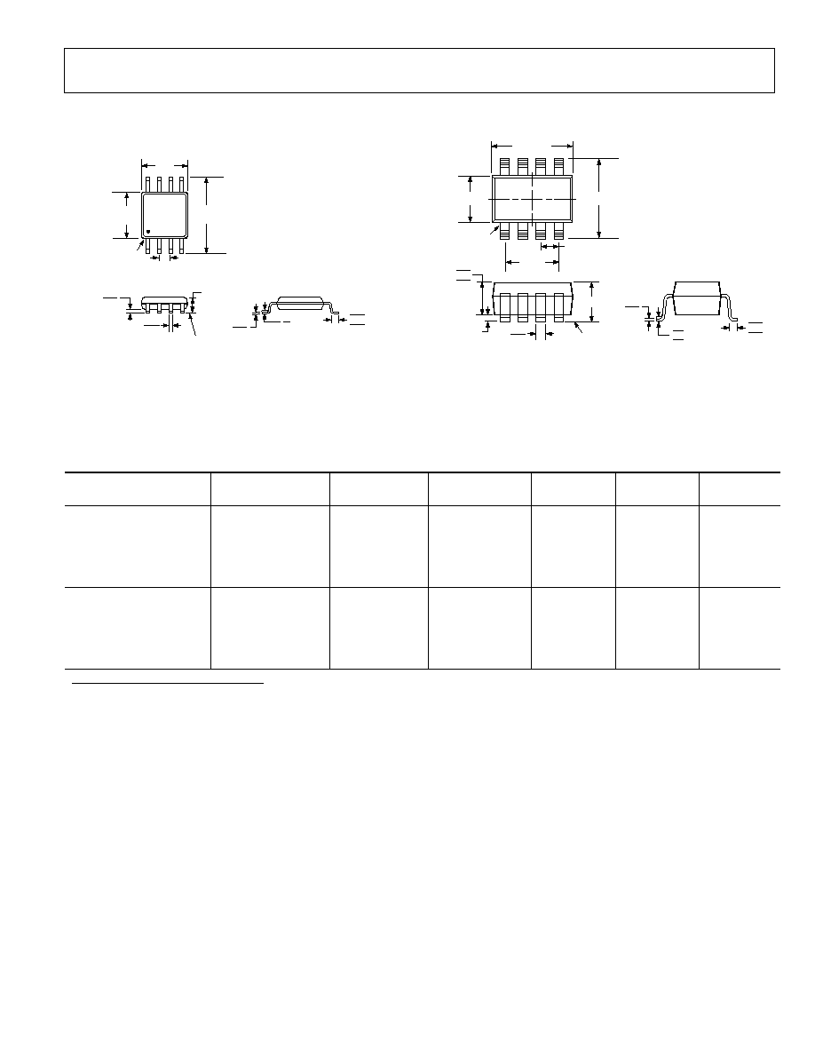
OUTLINE DIMENSIONS
0.80
0.60
0.40
8°
0°
4
8
5
4.90
BSC
PIN 1
0.65 BSC
3.00
BSC
SEATING
PLANE
0.15
0.00
0.38
0.22
1.10 MAX
3.00
BSC
COPLANARITY
0.10
0.23
0.08
COMPLIANT TO JEDEC STANDARDS MO-187AA
Figure 35. 8-Lead Mini Small Outline Package [MSOP]
(RM-8)
Dimensions shown in millimeters
1
3
5
6
2
8
4
7
2.90 BSC
PIN 1
1.60 BSC
1.95
BSC
0.65 BSC
0.38
0.22
0.10 MAX
0.90
0.87
0.84
SEATING
PLANE
1.00 MAX
0.20
0.08
0.55
0.45
0.35
8°
4°
0°
2.80 BSC
COMPLIANT TO JEDEC STANDARDS MO-193BA
Figure 36. 8-Lead Thin Small Outline Transistor Package [TSOT]
(UJ-8)
Dimensions shown in millimeters
ORDERING GUIDE
Model
Temperature
Range
Linearity
Error (LSB)
1
Package
Description
Package
Option
Branding
Quantity
AD7911ARM
-40°C to +85°C
±0.5 max
8-lead MSOP
RM-8
C1J
1
AD7911ARM-REEL
-40°C to +85°C
±0.5 max
8-lead MSOP
RM-8
C1J
3,000
AD7911ARM-REEL7
-40°C to +85°C
±0.5 max
8-lead MSOP
RM-8
C1J
1,000
AD7911AUJ-R2
-40°C to +85°C
±0.5 max
8-lead TSOT
UJ-8
C1J
250
AD7911AUJ-REEL7
-40°C to +85°C
±0.5 max
8-lead TSOT
UJ-8
C1J
3,000
AD7921ARM
-40°C to +85°C
±1.5 max
8-lead MSOP
RM-8
C1K
1
AD7921ARM-REEL
-40°C to +85°C
±1.5 max
8-lead MSOP
RM-8
C1K
3,000
AD7921ARM-REEL7
-40°C to +85°C
±1.5 max
8-lead MSOP
RM-8
C1K
1,000
AD7921AUJ-R2
-40°C to +85°C
±1.5 max
8-lead TSOT
UJ-8
C1K
250
AD7921AUJ-REEL7
-40°C to +85°C
±1.5 max
8-lead TSOT
UJ-8
C1K
3,000
1
Linearity error here refers to integral nonlinearity.

AD7911/AD7921
Rev. 0 | Page 26 of 28
NOTES

AD7911/AD7921
Rev. 0 | Page 27 of 28
NOTES

AD7911/AD7921
Rev. 0 | Page 28 of 28
NOTES
© 2004 Analog Devices, Inc. All rights reserved. Trademarks and
registered trademarks are the property of their respective owners.
D0435004/04(0)
Document Outline
- FEATURES
- APPLICATIONS
- GENERAL DESCRIPTION
- FUNCTIONAL BLOCK DIAGRAM
- PRODUCT HIGHLIGHTS
- þÿ
- þÿ
- þÿ
- þÿ
- þÿ
- þÿ
- þÿ
- þÿ
- þÿ
- þÿ