Äîêóìåíòàöèÿ è îïèñàíèÿ www.docs.chipfind.ru
High Common-Mode Voltage,
Single-Supply Difference Amplifier
AD8202
Rev. A
Information furnished by Analog Devices is believed to be accurate and reliable.
However, no responsibility is assumed by Analog Devices for its use, nor for any
infringements of patents or other rights of third parties that may result from its use.
Specifications subject to change without notice. No license is granted by implication
or otherwise under any patent or patent rights of Analog Devices. Trademarks and
registered trademarks are the property of their respective owners.
One Technology Way, P.O. Box 9106, Norwood, MA 02062-9106, U.S.A.
Tel: 781.329.4700
www.analog.com
Fax: 781.326.8703
© 2004 Analog Devices, Inc. All rights reserved.
FEATURES
High common-mode voltage range
-8 V to +28 V at a 5 V supply voltage
Operating temperature range: -40°C to +125°C
Supply voltage range: 3.5 V to 12 V
Low-pass filter (1-pole or 2-pole)
EXCELLENT AC AND DC PERFORMANCE
±1 mV voltage offset
±1 ppm/°C typ gain drift
80 dB CMRR min dc to 10 kHz
PLATFORMS
Transmission control
Diesel injection control
Engine management
Adaptive suspension control
Vehicle dynamics control
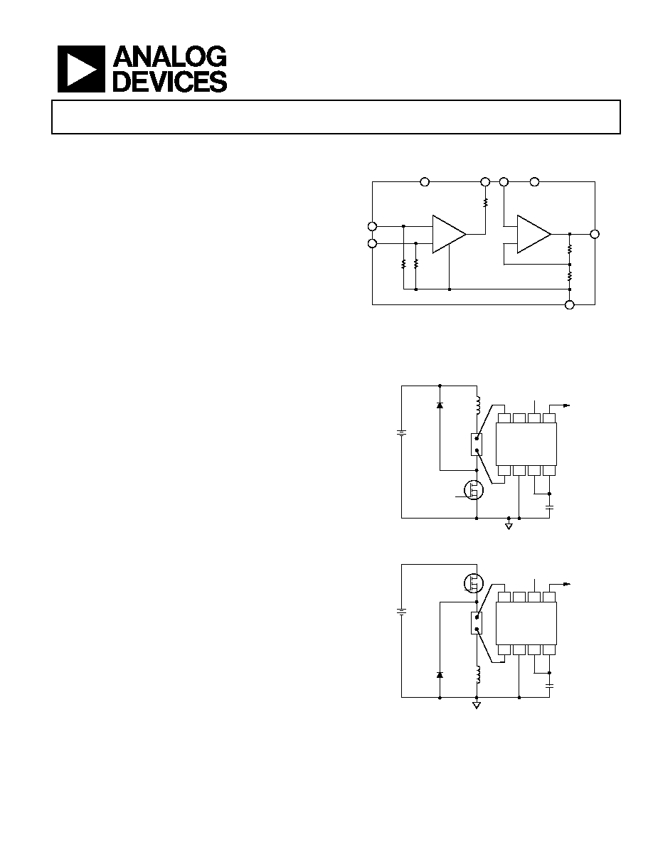
FUNCTIONAL BLOCK DIAGRAM
A1
+IN
IN
200k
200k
100k
A2
+IN
IN
G =
×
10
G =
×
2
AD8202
10k
10k
+IN
IN
GND
OUT
NC
A1
A2
+V
S
NC = NO CONNECT
2
5
6
4
7
8
1
3
04981-0-001
Figure 1. SOIC (R) Package Die Form
GENERAL DESCRIPTION
The AD8202 is a single-supply difference amplifier for amplifying
and low-pass filtering small differential voltages in the presence of a
large common-mode voltage. The input CMV range extends from
-8 V to +28 V at a typical supply voltage of 5 V.
The AD8202 is offered in die and packaged form. Both package
options are specified over a wide temperature range of -40°C to
+125°C, making the AD8202 well-suited for use in many auto-
motive platforms.
Automotive platforms demand precision components for better
system control. The AD8202 provides excellent ac and dc
performance, which keeps errors to a minimum in the user's
system. Typical offset and gain drift in the SOIC package are
5 µV/°C and 1 ppm/°C, respectively. The device also delivers a
minimum CMRR of 80 dB from dc to 10 kHz.
The AD8202 features an externally accessible 100 k resistor at
the output of the preamp A1, which can be used for low-pass
filter applications and for establishing gains other than 20.
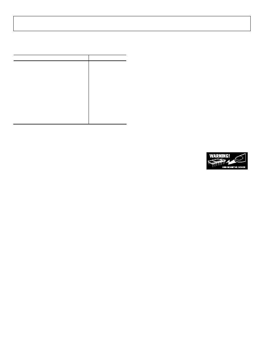
GND
NC
IN
+IN
A1
+V
S
A2
OUT
AD8202
5V
OUTPUT
INDUCTIVE
LOAD
POWER
DEVICE
4-TERM
SHUNT
CLAMP
DIODE
BATTERY
14V
COMMON
NC = NO CONNECT
04981-0-002
Figure 2. High-Line Current Sensor
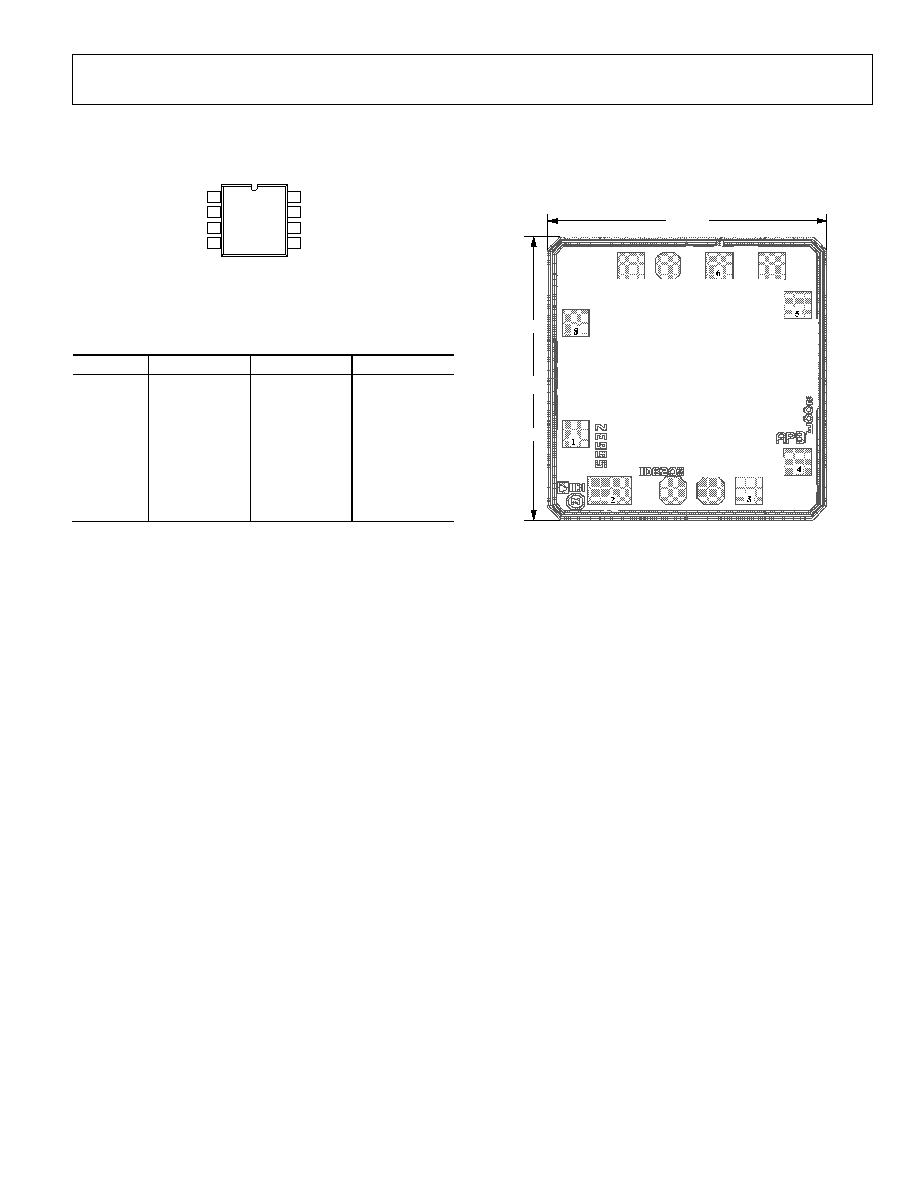
GND
NC
IN
+IN
A1
+V
S
A2
OUT
AD8202
5V
OUTPUT
INDUCTIVE
LOAD
POWER
DEVICE
4-TERM
SHUNT
CLAMP
DIODE
BATTERY
14V
COMMON
NC = NO CONNECT
04981-0-003
Figure 3. Low-Line Current Sensor

AD8202
Rev. A | Page 2 of 12
TABLE OF CONTENTS
Specifications--Single Supply ......................................................... 3
Absolute Maximum Ratings............................................................ 4
ESD Caution.................................................................................. 4
Pin Configuration and Function Descriptions............................. 5
Typical Performance Characteristics ............................................. 6
Theory of Operation ........................................................................ 8
Applications....................................................................................... 9
Current Sensing ............................................................................ 9
Gain Adjustment........................................................................... 9
Gain Trim .................................................................................... 10
Low-Pass Filtering...................................................................... 10
High-Line Current Sensing with LPF
and Gain Adjustment................................................................. 11
Driving Charge Redistribution ADCs ..................................... 11
Outline Dimensions ....................................................................... 12
Ordering Guide .......................................................................... 12
REVISION HISTORY
11/04--Rev. 0 to a Rev. A
Changes to the Features ................................................................... 1
Changes to the General Description.............................................. 1
Changes to Specifications (Table 1) ............................................... 3
Changes to Absolute Maximum Ratings (Table 2)....................... 4
Changes to Pin Function Descriptions (Table 3) ......................... 5
Changes to Figure 5.......................................................................... 5
Changes to Figure 9 and Figure 10................................................. 6
Updated Outline Dimensions ....................................................... 12
Changes to the Ordering Guide.................................................... 12
7/04--Revision 0: Initial Version

AD8202
Rev. A | Page 3 of 12
SPECIFICATIONS--SINGLE SUPPLY
T
A
= operating temperature range, V
S
= 5 V, unless otherwise noted.
Table 1.
AD8202 SOIC
AD8202 DIE
Parameter Conditions
Min
Typ
Max
Min
Typ
Max
Unit
SYSTEM
GAIN
Initial
20
20
V/V
Error
0.02 V
OUT
4.8 V dc
-0.3
+0.3
-0.3
+0.3
%
vs. Temperature
1
20
1
30
ppm/°C
VOLTAGE
OFFSET
Input Offset (RTI)
V
CM
= 0.15 V; 25°C
-1
+1
-1
+1
mV
vs. Temperature
-40°C to +125°C
-10 +0.3 +10 -10 +0.3 +10 µV/°C
-40°C to +150°C
-15
+5
+15
µV/°C
INPUT
Input
Impedance
Differential
260 325 390 260 325 390 k
Common-Mode
135 170 205 135 170 205 k
CMV Continuous
-8
+28
-8
+28
V
Common-Mode Rejection
1
V
CM
= 0 V to 10 V
f = DC
82
82
dB
f = 1 kHz
82
82
dB
f = 10 kHz
2
80
80
dB
PREAMPLIFIER
Gain
10
10
V/V
Gain Error
-0.3
+0.3
-0.3
+0.3
%
Output Voltage Range
0.02
4.8
0.02
4.8
V
Output Resistance
97
100
103
97
100
103
k
OUTPUT
BUFFER
Gain
2
2
V/V
Gain Error
0.02 V
OUT
4.8 V dc
-0.3
+0.3
-0.3
+0.3
%
Output Voltage Range
0.02
4.8
0.02
4.8
V
Input Bias Current
40
40
nA
Output Resistance
2
2
DYNAMIC
RESPONSE
System Bandwidth
V
IN
= 0.01 V dc, V
OUT
= 0.2 V p-p
30
50
30
50
kHz
Slew Rate
V
IN
= 0.2 V dc, V
OUT
= 4 V Step
0.28
0.28
V/µs
NOISE
0.1 Hz to 10 Hz
10
10
µV p-p
Spectral Density, 1 kHz (RTI)
275
275
nV/Hz
POWER
SUPPLY
Operating Range
3.5
12
3.5
12
V
Quiescent Current vs. Temperature
V
O
= 0.1 V dc
0.25
1.0
0.25
1.0
mA
PSRR V
S
= 3.5 V to 12 V
75
83
75
83
dB
TEMPERATURE
RANGE
For Specified Performance
-40
+125
-40
+150
°C
1
Source imbalance < 2 .
2
The AD8202 preamplifier exceeds 80 dB CMRR at 10 kHz. However, since the signal is available only by way of a 100 k resistor, even the small amount of pin-to-pin
capacitance between Pins 1, 8 and 3, 4 may couple an input common-mode signal larger than the greatly attenuated preamplifier output. The effect of pin-to-pin
coupling may be neglected in all applications by using filter capacitors at Node 3.
AD8202
Rev. A | Page 4 of 12
ABSOLUTE MAXIMUM RATINGS
Table 2.
Parameter Rating
Supply Voltage
12.5 V
Transient Input Voltage (400 ms)
44 V
Continuous Input Voltage
(Common Mode)
35 V
Reversed Supply Voltage Protection
0.3 V
Operating Temperature Range
Die
-40°C to +150°C
SOIC
-40°C to +125°C
Storage Temperature
-65°C to +150°C
Output Short-Circuit Duration Indefinite
Lead Temperature Range
(Soldering 10 sec)
300°C
Stresses above those listed under Absolute Maximum Ratings
may cause permanent damage to the device. This is a stress
rating only and functional operation of the device at these or
any other conditions above those indicated in the operational
section of this specification is not implied. Exposure to absolute
maximum rating conditions for extended periods may affect
device reliability.
ESD CAUTION
ESD (electrostatic discharge) sensitive device. Electrostatic charges as high as 4000 V readily accumulate on
the human body and test equipment and can discharge without detection. Although this product features
proprietary ESD protection circuitry, permanent damage may occur on devices subjected to high energy
electrostatic discharges. Therefore, proper ESD precautions are recommended to avoid performance
degradation or loss of functionality.
AD8202
Rev. A | Page 5 of 12
PIN CONFIGURATION AND FUNCTION DESCRIPTIONS
IN
1
GND
2
A1
3
A2
4
+IN
8
NC
7
+V
S
6
OUT
5
NC = NO CONNECT
AD8202
TOP VIEW
(Not to Scale)
04981-0-004
Figure 4. 8-Lead SOIC
Table 3. 8-Lead SOIC Pin Function Descriptions
Pin No.
Mnemonic
X
Y
1 -IN
-409.0 -205.2
2 GND -244.6 -413.0
3 A1
+229.4 -413.0
4 A2
+410.0 -308.6
5 OUT +410.0 +272.4
6 +Vs +121.0 +417.0
7 NC
NA
NA
8 +IN
-409.0 +205.2
04981-0-005
1036
µ
m
+V
S
1048
µ
m
A1
GND
OUT
A2
+IN
IN
Figure 5. Metallization Photograph
AD8202
Rev. A | Page 6 of 12
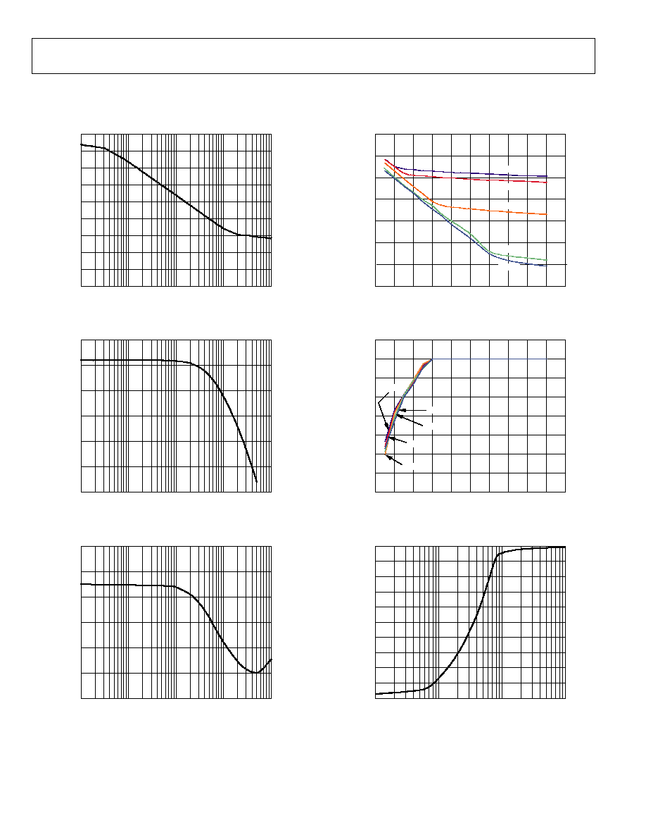
TYPICAL PERFORMANCE CHARACTERISTICS
T
A
= 25°C, V
S
= 5 V, V
CM
= 0 V, R
L
= 10 k, unless otherwise noted.
FREQUENCY (Hz)
P
S
RR (dB)
90
70
80
50
60
40
10
20
30
0
10
100
1k
10k
100k
04981-0-006
Figure 6. Power Supply Rejection Ratio vs. Frequency
FREQUENCY (Hz)
OUTP
UT (dB)
30
25
20
15
5
10
0
100
1k
10k
100k
1M
04981-0-007
Figure 7. AD8202 Bandwidth
FREQUENCY (Hz)
CMRR (dB)
100
95
90
85
75
80
70
10
100
1k
10k
100k
04981-0-008
Figure 8. Common-Mode Rejection Ratio vs. Frequency
POWER SUPPLY (V)
COMMON-MODE
V
O
LTAGE
(V
)
0
5
10
15
20
25
30
35
3
4
5
6
7
8
9
10
11
12
13
04981-0-009
55
°
C
40
°
C
+25
°
C
+125
°
C
+150
°
C
Figure 9. Negative Common-Mode Voltage vs. Voltage Supply
POWER SUPPLY (V)
COMMON-MODE
V
O
LTAGE
(V
)
40
35
25
30
20
5
10
15
0
3
6
5
4
8
7
10
9
11
12
04981-0-010
13
40
°
C
55
°
C
+25
°
C
+125
°
C
+150
°
C
Figure 10. Positive Common-Mode Voltage vs. Voltage Supply
LOAD RESISTANCE (
)
OUTPUT SW
ING (
V
)
5.0
4.0
4.5
3.5
3.0
2.5
0.5
1.0
1.5
2.0
0
10
100
1k
10k
04981-0-011
Figure 11. Output Swing vs. Load Resistance
AD8202
Rev. A | Page 7 of 12
13
SUPPLY VOLTAGE (V)
OUTP
UT MINUS
S
U
P
P
LY
(mV
)
0
10
20
30
40
50
60
70
3
6
5
4
8
7
10
9
11
12
04981-0-012
10k LOAD
INF LOAD
Figure 12. Swing Minus Supply vs. Supply Voltage
2
1
CH1 500mV
50mV
M 20
µ
s 2.5MS/s 400NS/PT
A CH1 1.73V
CH2
04981-0-013
OUTPUT
INPUT
Figure 13. Pulse Response
AD8202
Rev. A | Page 8 of 12
THEORY OF OPERATION
The AD8202 consists of a preamp and buffer arranged as shown
in Figure 14. Like-named resistors have equal values.
The preamp incorporates a dynamic bridge (subtractor) circuit.
Identical networks (within the shaded areas), consisting of R
A
,
R
B
, R
C
, and R
G
, attenuate input signals applied to Pins 1 and 8.
Note that when equal amplitude signals are asserted at inputs 1
and 8, and the output of A1 is equal to the common potential
(i.e., zero), the two attenuators form a balanced-bridge network.
When the bridge is balanced, the differential input voltage at A1,
and thus its output, is zero.
Any common-mode voltage applied to both inputs keeps the
bridge balanced and the A1 output at zero. Because the resistor
networks are carefully matched, the common-mode signal
rejection approaches this ideal state.
However, if the signals applied to the inputs differ, the result is a
difference at the input to A1. A1 responds by adjusting its output
to drive R
B
, by way of R
G
, to adjust the voltage at its inverting
input until it matches the voltage at its noninverting input.
By attenuating voltages at Pins 1 and 8, the amplifier inputs are
held within the power supply range, even if Pin 1 and Pin 8
input levels exceed the supply, or fall below common (ground).
The input network also attenuates normal (differential) mode
voltages. R
C
and R
G
form an attenuator that scales A1 feedback,
forcing large output signals to balance relatively small differen-
tial inputs. The resistor ratios establish the preamp gain at 10.
Because the differential input signal is attenuated and then
amplified to yield an overall gain of 10, Amplifier A1 operates at
a higher noise gain, multiplying deficiencies such as input offset
voltage and noise with respect to Pins 1 and 8.
A1
A3
R
CM
R
CM
(TRIMMED)
100k
R
A
IN
R
G
R
C
R
B
R
A
R
C
R
B
R
G
+IN
COM
A2
R
F
R
F
AD8202
5
4
3
1
2
8
04981-0-014
Figure 14. Simplified Schematic
To minimize these errors while extending the common-mode
range, a dedicated feedback loop is employed to reduce the
range of common-mode voltage applied to A1 for a given over-
all range at the inputs. By offsetting the range of voltage applied
to the compensator, the input common-mode range is also
offset to include voltages more negative than the power supply.
Amplifier A3 detects the common-mode signal applied to A1
and adjusts the voltage on the matched R
CM
resistors to reduce
the common-mode voltage range at the A1 inputs. By adjusting
the common voltage of these resistors, the common-mode input
range is extended while, at the same time, the normal mode
signal attenuation is reduced, leading to better performance
referred to input.
The output of the dynamic bridge taken from A1 is connected
to Pin 3 by way of a 100 k series resistor, provided for low-
pass filtering and gain adjustment. The resistors in the input
networks of the preamp and the buffer feedback resistors are
ratio trimmed for high accuracy.
The output of the preamp drives a gain-of-2 buffer amplifier,
A2, implemented with carefully matched feedback resistors R
F
.
The 2-stage system architecture of the AD8202 enables the user
to incorporate a low-pass filter prior to the output buffer. By
separating the gain into two stages, a full-scale, rail-to-rail signal
from the preamp can be filtered at Pin 3, and a half-scale signal,
resulting from filtering, can be restored to full scale by the
output buffer amp. The source resistance seen by the inverting
input of A2 is approximately 100 k to minimize the effects of
A2's input bias current. However, this current is quite small and
errors resulting from applications that mismatch the resistance
are correspondingly small.
AD8202
Rev. A | Page 9 of 12
APPLICATIONS
The AD8202 difference amplifier is intended for applications
where it is required to extract a small differential signal in the
presence of large common-mode voltages. The input resistance
is nominally 170 k, and the device can tolerate common-mode
voltages higher than the supply voltage and lower than ground.
The open collector output stage sources current to within
20 mV of ground and to within 200 mV of V
S
.
CURRENT SENSING
High-Line, High Current Sensing
Basic automotive applications making use of the large common-
mode range are shown in Figure 2 and Figure 3. The capability
of the device to operate as an amplifier in primary battery sup-
ply circuits is shown in Figure 2; Figure 3 illustrates the ability
of the device to withstand voltages below system ground.
Low Current Sensing
The AD8202 can also be used in low current sensing applications,
such as the 4 to 20 mA current loop shown in Figure 15. In such
applications, the relatively large shunt resistor can degrade the
common-mode rejection. Adding a resistor of equal value on the
low impedance side of the input corrects for this error.
5V
OUTPUT
10
1%
10
1%
NC = NO CONNECT
+
GND
NC
IN
+IN
A1
+V
S
A2
OUT
AD8202
04981-0-015
Figure 15. 4 to 20 mA Current Loop Receiver
GAIN ADJUSTMENT
The default gain of the preamplifier and buffer are ×10 and ×2,
respectively, resulting in a composite gain of ×20. With the
addition of external resistor(s) or trimmer(s), the gain may be
lowered, raised, or finely calibrated.
Gains Less than 20
Since the preamplifier has an output resistance of 100 k, an
external resistor connected from Pins 3 and 4 to GND decreases
the gain by a factor R
EXT
/(100 k + R
EXT
) (see Figure 16).
10k
10k
100k
A2
A1
GND
IN
OUT
+V
S
NC
+IN
AD8202
OUT
+V
S
R
EXT
V
CM
V
DIFF
2
GAIN =
20R
EXT
R
EXT
+ 100k
R
EXT
= 100k
GAIN
20 GAIN
V
DIFF
2
NC = NO CONNECT
04981-0-016
Figure 16. Adjusting for Gains Less than 20
The overall bandwidth is unaffected by changes in gain by using
this method, although there may be a small offset voltage due to
the imbalance in source resistances at the input to the buffer. In
many cases this can be ignored, but if desired, it can be nulled
by inserting a resistor equal to 100 k minus the parallel sum of
R
EXT
and 100 k, in series with Pin 4. For example, with R
EXT
=
100 k (yielding a composite gain of ×10), the optional offset
nulling resistor is 50 k.
Gains Greater than 20
Connecting a resistor from the output of the buffer amplifier to
its noninverting input, as shown in Figure 17, increases the gain.
The gain is now multiplied by the factor R
EXT
/(R
EXT
- 100 k);
for example, it is doubled for R
EXT
= 200 k. Overall gains as
high as 50 are achievable in this way. Note that the accuracy of
the gain becomes critically dependent on the resistor value at
high gains. Also, the effective input offset voltage at Pin 1 and
Pin 8 (about six times the actual offset of A1) limits the part's
use in high gain, dc-coupled applications.
10k
10k
100k
A2
A1
GND
IN
OUT
+V
S
NC
+IN
AD8202
OUT
+V
S
R
EXT
V
CM
V
DIFF
2
GAIN =
20R
EXT
R
EXT
100k
R
EXT
= 100k
GAIN
GAIN 20
V
DIFF
2
NC = NO CONNECT
04981-
0-
017
Figure 17. Adjusting for Gains Greater than 20
AD8202
Rev. A | Page 10 of 12
GAIN TRIM
Figure 18 shows a method for incremental gain trimming by
using a trim potentiometer and external resistor R
EXT
.
The following approximation is useful for small gain ranges.
G (10 M ÷ R
EXT
)%
Thus, the adjustment range is ±2% for R
EXT
= 5 M; ±10% for
R
EXT
= 1 M, and so on.
5V
OUT
R
EXT
GAIN TRIM
20k
MIN
V
CM
V
DIFF
2
V
DIFF
2
NC = NO CONNECT
GND
NC
IN
+IN
A1
+V
S
A2
OUT
AD8202
04981-0-018
Figure 18. Incremental Gain Trim
Internal Signal Overload Considerations
When configuring gain for values other than 20, the maximum
input voltage with respect to the supply voltage and ground
must be considered, since either the preamplifier or the output
buffer reaches its full-scale output (approximately V
S
0.2 V)
with large differential input voltages. The input of the AD8202
is limited to (V
S
0.2) ÷ 10 for overall gains 10, since the pre-
amplifier, with its fixed gain of ×10, reaches its full-scale output
before the output buffer. For gains greater than 10, the swing at
the buffer output reaches its full scale first and limits the
AD8202 input to (V
S
0.2) ÷ G, where G is the overall gain.
LOW-PASS FILTERING
In many transducer applications, it is necessary to filter the sig-
nal to remove spurious high frequency components including
noise, or to extract the mean value of a fluctuating signal with a
peak-to-average ratio (PAR) greater than unity. For example, a
full-wave rectified sinusoid has a PAR of 1.57, a raised cosine
has a PAR of 2, and a half-wave sinusoid has a PAR of 3.14.
Signals having large spikes may have PARs of 10 or more.
When implementing a filter, the PAR should be considered so
that the output of the AD8202 preamplifier (A1) does not clip
before A2, since this nonlinearity would be averaged and appear
as an error at the output. To avoid this error, both amplifiers
should be made to clip at the same time. This condition is
achieved when the PAR is no greater than the gain of the sec-
ond amplifier (2 for the default configuration). For example, if a
PAR of 5 is expected, the gain of A2 should be increased to 5.
Low-pass filters can be implemented in several ways by using
the features provided by the AD8202. In the simplest case, a
single-pole filter (20 dB/decade) is formed when the output of
A1 is connected to the input of A2 via the internal 100 k resis-
tor by strapping Pins 3 and 4 and a capacitor added from this
node to ground, as shown in Figure 19. If a resistor is added
across the capacitor to lower the gain, the corner frequency
increases; it should be calculated using the parallel sum of the
resistor and 100 k.
5V
V
CM
V
DIFF
2
V
DIFF
2
NC = NO CONNECT
C
GND
NC
IN
+IN
A1
+V
S
A2
OUT
AD8202
04981-0-019
OUTPUT
F
C
=
1
2
C10
5
C IN FARADS
Figure 19. Single-Pole, Low-Pass Filter Using the Internal 100 k Signal
If the gain is raised using a resistor, as shown in Figure 17, the
corner frequency is lowered by the same factor as the gain is
raised. Thus, using a resistor of 200 k (for which the gain
would be doubled), the corner frequency is now 0.796 Hz µF
(0.039 µF for a 20 Hz corner frequency.)
5V
V
CM
V
DIFF
2
V
DIFF
2
NC = NO CONNECT
C
GND
NC
IN
+IN
A1
+V
S
A2
OUT
AD8202
04981-0-020
OUT
C
255k
FC = 1Hz
µ
F
Figure 20. 2-Pole, Low-Pass Filter
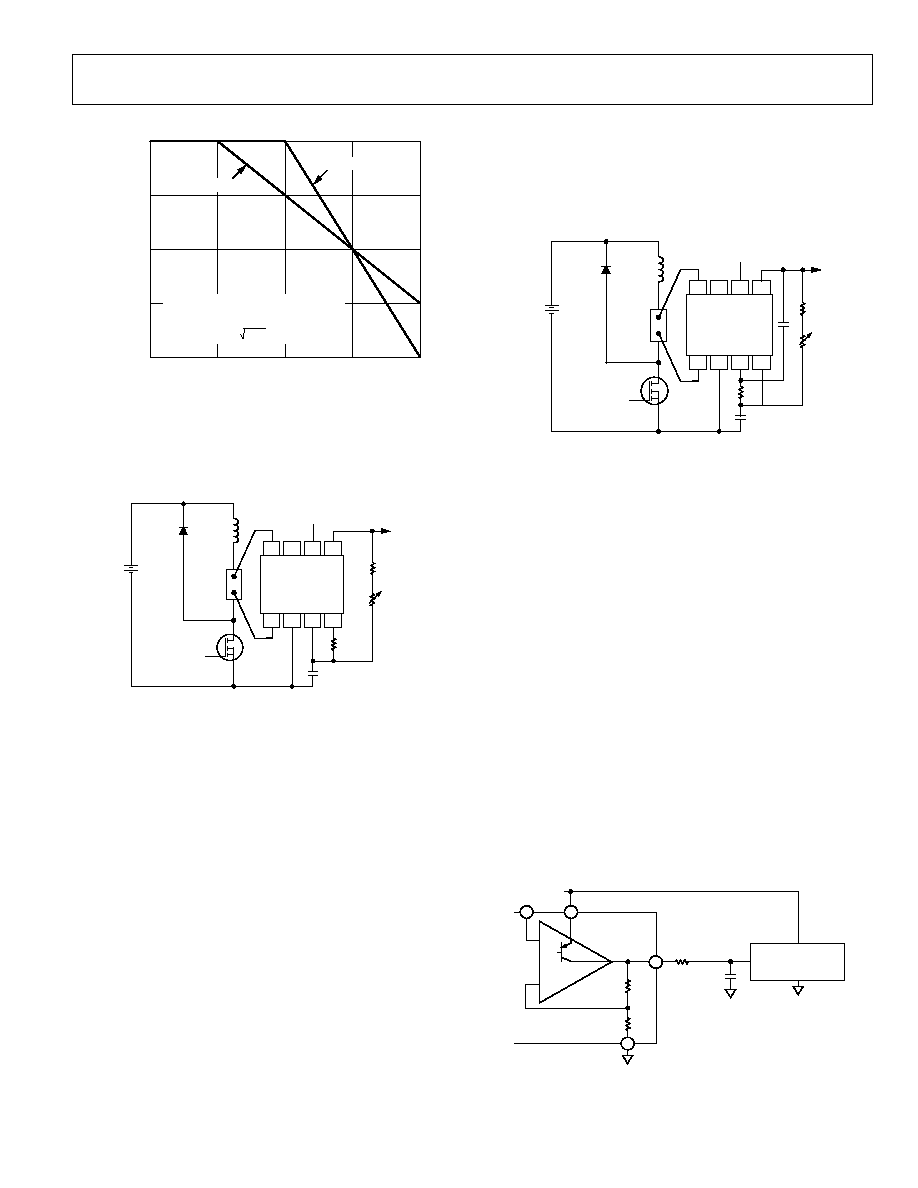
A 2-pole filter (with a roll-off of 40 dB/decade) can be imple-
mented using the connections shown in Figure 20. This is a
Sallen-Key form based on a ×2 amplifier. It is useful to remember
that a 2-pole filter with a corner frequency f
2
and a 1-pole filter
with a corner at f
1
have the same attenuation at the frequency
(f
2
2
/f
1
). The attenuation at that frequency is 40 log (f
2
/f
1
), which is
illustrated in Figure 21. Using the standard resistor value shown
and equal capacitors (Figure 20), the corner frequency is conven-
iently scaled at 1 Hz µF (0.05 µF for a 20 Hz corner). A maximally
flat response occurs when the resistor is lowered to 196 k and
the scaling is then 1.145 Hz µF. The output offset is raised by
approximately 5 mV (equivalent to 250 µV at the input pins).
AD8202
Rev. A | Page 11 of 12
40LOG (f
2
/f
1
)
f
1
ATTE
NUATION
f
2
f
2
2
/f
1
FREQUENCY
A 1-POLE FILTER, CORNER f
1
, AND
A 2-POLE FILTER, CORNER f
2
, HAVE
THE SAME ATTENUATION 40LOG (f
2
/f
1
)
AT FREQUENCY f
2
2
/f
1
20dB/DECADE
40dB/DECADE
04981-0-021
Figure 21. Comparative Responses of 1-Pole and 2-Pole Low-Pass Filters
HIGH-LINE CURRENT SENSING WITH LPF AND
GAIN ADJUSTMENT
Figure 22 is another refinement of Figure 2, including gain
adjustment and low-pass filtering.
GND
NC
IN
+IN
A1
+V
S
A2
OUT
AD8202
5V
INDUCTIVE
LOAD
POWER
DEVICE
4-TERM
SHUNT
CLAMP
DIODE
BATTERY
14V
NC = NO CONNECT
COMMON
04981-
0-
022
C
OUT
4V/AMP
5% CALIBRATION RANGE
f
C
= 0.796Hz
µ
F
(0.22
µ
F FOR f
C
= 3.6Hz)
V
OS/IB
NULL
191k
20k
Figure 22. High-Line Current Sensor Interface;
Gain = ×40, Single-Pole, Low-Pass Filter
A power device that is either on or off controls the current in
the load. The average current is proportional to the duty cycle
of the input pulse and is sensed by a small value resistor. The
average differential voltage across the shunt is typically 100 mV,
although its peak value is higher by an amount that depends on
the inductance of the load and the control frequency. The
common-mode voltage, on the other hand, extends from
roughly 1 V above ground for the on condition to about 1.5 V
above the battery voltage in the off condition. The conduction
of the clamping diode regulates the common-mode potential
applied to the device. For example, a battery spike of 20 V may
result in an applied common-mode potential of 21.5 V to the
input of the devices.
To produce a full-scale output of 4 V, a gain ×40 is used, adjust-
able by ±5% to absorb the tolerance in the shunt. There is
sufficient headroom to allow 10% overrange (to 4.4 V). The
roughly triangular voltage across the sense resistor is averaged
by a 1-pole, low-pass filter, here set with a corner frequency of
3.6 Hz, which provides about 30 dB of attenuation at 100 Hz. A
higher rate of attenuation can be obtained using a 2-pole filter
with f
C
= 20 Hz, as shown in Figure 23. Although this circuit
uses two separate capacitors, the total capacitance is less than
half that needed for the 1-pole filter.
GND
NC
IN
+IN
A1
+V
S
A2
OUT
AD8202
5V
INDUCTIVE
LOAD
POWER
DEVICE
4-TERM
SHUNT
CLAMP
DIODE
BATTERY
14V
NC = NO CONNECT
COMMON
04981-
0-
023
f
C
= 1Hz
µ
F
(0.05
µ
F FOR f
C
= 20Hz)
C
OUTPUT
127k
C
432k
50k
Figure 23. 2-Pole Low-Pass Filter
DRIVING CHARGE REDISTRIBUTION ADCS
When driving CMOS ADCs such as those embedded in popular
microcontrollers, the charge injection (Q) can cause a
significant deflection in the output voltage of the AD8202.
Though generally of short duration, this deflection may persist
until after the sample period of the ADC has expired due to the
relatively high open-loop output impedance of the AD8202.
Including an R-C network in the output can significantly reduce
the effect. The capacitor helps to absorb the transient charge,
effectively lowering the high frequency output impedance of the
AD8202. For these applications, the output signal should be
taken from the midpoint of the R
LAG
- C
LAG
combination as
shown in Figure 24.
Since the perturbations from the analog-to-digital converter are
small, the output impedance of the AD8202 appears to be low. The
transient response, therefore, has a time constant governed by the
product of the two LAG components, C
LAG
× R
LAG
. For the values
shown in Figure 24, this time constant is programmed at approxi-
mately 10 µs. Therefore, if samples are taken at several tens of
microseconds or more, there is negligible charge stack-up.
+IN
IN
10k
10k
AD8202
5V
R
LAG
1k
C
LAG
0.01
µ
F
MICROPROCESSOR
A/D
A2
2
4
6
5
04981-0-024
Figure 24. Recommended Circuit for Driving CMOS A/D
AD8202
Rev. A | Page 12 of 12
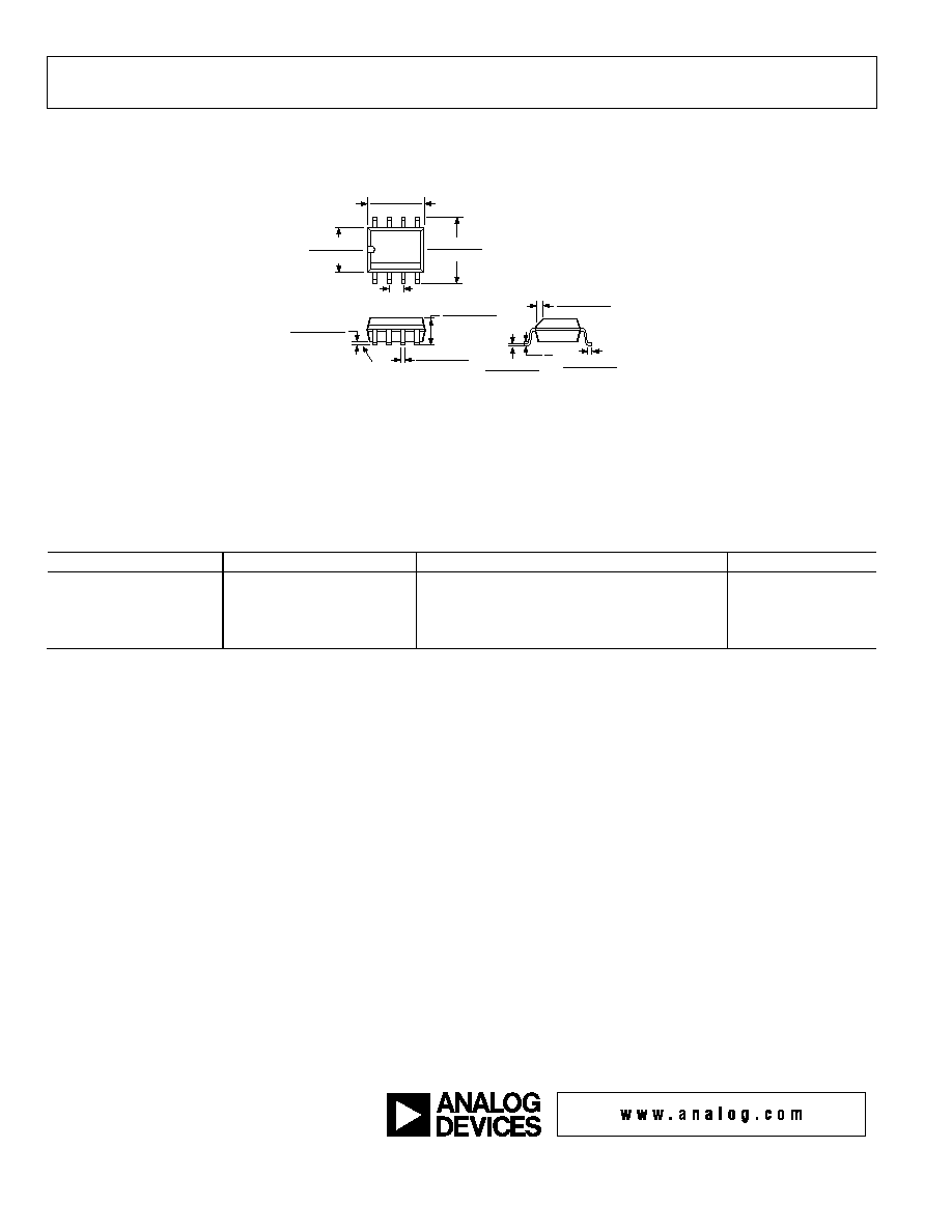
OUTLINE DIMENSIONS
0.25 (0.0098)
0.17 (0.0067)
1.27 (0.0500)
0.40 (0.0157)
0.50 (0.0196)
0.25 (0.0099)
×
45°
8°
0°
1.75 (0.0688)
1.35 (0.0532)
SEATING
PLANE
0.25 (0.0098)
0.10 (0.0040)
4
1
8
5
5.00 (0.1968)
4.80 (0.1890)
4.00 (0.1574)
3.80 (0.1497)
1.27 (0.0500)
BSC
6.20 (0.2440)
5.80 (0.2284)
0.51 (0.0201)
0.31 (0.0122)
COPLANARITY
0.10
CONTROLLING DIMENSIONS ARE IN MILLIMETERS; INCH DIMENSIONS
(IN PARENTHESES) ARE ROUNDED-OFF MILLIMETER EQUIVALENTS FOR
REFERENCE ONLY AND ARE NOT APPROPRIATE FOR USE IN DESIGN
COMPLIANT TO JEDEC STANDARDS MS-012AA
Figure 25. 8-Lead Standard Small Outline Package [SOIC]
Narrow Body (R-8)
Dimensions shown in millimeters (inches)
ORDERING GUIDE
Model
Temperature Package
Package Description
Package Outline
AD8202YR
-40°C to +125°C
8 Lead Standard Small Outline Package (SOIC)
R-8
AD8202YR-REEL
-40°C to +125°C
8-Lead Standard Small Outline Package (SOIC)
R-8
AD8202YR-REEL7
-40°C to +125°C
8-Lead Standard Small Outline Package (SOIC)
R-8
AD8202YCSURF
Die
© 2004 Analog Devices, Inc. All rights reserved. Trademarks and
registered trademarks are the property of their respective owners.
D04981011/04(A)
Document Outline