 | ÐлекÑÑоннÑй компоненÑ: AD8210YRZ | СкаÑаÑÑ:  PDF PDF  ZIP ZIP |
AD8210 High-Side, Bidirectional Current Shunt Monitor Data Sheet (Rev. PrB)
High-Side, Bidirectional
Current Shunt Monitor
Preliminary Technical Data
AD8210
Rev. PrB
Information furnished by Analog Devices is believed to be accurate and reliable.
However, no responsibility is assumed by Analog Devices for its use, nor for any
infringements of patents or other rights of third parties that may result from its use.
Specifications subject to change without notice. No license is granted by implication
or otherwise under any patent or patent rights of Analog Devices. Trademarks and
registered trademarks are the property of their respective owners.
One Technology Way, P.O. Box 9106, Norwood, MA 02062-9106, U.S.A.
Tel: 781.329.4700
www.analog.com
Fax: 781.326.8703
© 2005 Analog Devices, Inc. All rights reserved.
FEATURES
Precision bidirectional current sensing
High common-mode voltage range
-2 V to +65 V operating
Gain = 20
CMRR = 100 dB
Wide operating temperature range
Die: -40°C to +150°C
8-lead SOIC: -40°C to +125°C
Adjustable offset
Available in SOIC and die form
EXCELLENT AC AND DC PERFORMANCE
5 µV/°C offset drift
30 ppm/°C gain drift
80 dB CMRR dc to 10 kHz
APPLICATIONS
42 V dc-to-dc converter current sensing
High-side current sensing
Motor controls
Transmission controls
Diesel injection controls
Engine management
Suspension controls
Vehicle dynamic controls
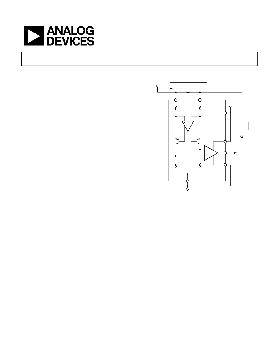
TYPICAL OPERATING CIRCUIT
LOAD
AD8210
VOUT
G = +20
V
SUPPLY
I
S
R
S
+IN
IN
V
S
V+
V
REF
1
V
REF
2
GND
05147-001
Figure 1.
GENERAL DESCRIPTION
The AD8210 is a high-side, single-supply, bidirectional current
shunt monitor that features a wide input, common-mode volt-
age range of -2 V to +65 V, high bandwidth, a set gain of 20, and
a typical 5 V supply voltage.
The AD8210 is offered in die and packaged form. The operating
temperature range for the die is 25°C higher (up to 150°C) than
that of the packaged part, which enables the user to apply the
AD8210 in high temperature applications.
Excellent ac and dc performance over temperature keeps errors
in the measurement loop to a minimum. Offset drift is typically
below 5 µV/°C, and the gain drift is typically below 30 ppm/°C.
Bidirectional current measurement is achieved by offsetting the
output between 0.05 V and 4.8 V with a 5 V supply. With the
V
REF
2 pin connected to the V+ pin, and the V
REF
1 pin connected
to the GND pin, the output is set at half scale. Attaching both
V
REF
pins to GND causes the output to be unipolar, starting near
ground. Attaching both V
REF
pins to V+ causes the output to be
unipolar starting near V+. Other offsets can be obtained by
applying an external voltage to V
REF
1 and V
REF
2 pins.

AD8210
Preliminary Technical Data
Rev. PrB | Page 2 of 12
TABLE OF CONTENTS
Specifications..................................................................................... 3
Absolute Maximum Ratings............................................................ 4
ESD Caution.................................................................................. 4
Pin Configuration and Function Descriptions............................. 5
Typical Performance Characteristics ............................................. 6
Theory of Operation ........................................................................ 8
Output Offset Adjustment............................................................... 9
Unidirectional Operation............................................................ 9
Ground Referenced Output ........................................................ 9
V+ Referenced Output................................................................. 9
Bidirectional Operation................................................................9
External Reference Output........................................................ 10
Splitting an External Reference ................................................ 10
Splitting the Supply .................................................................... 10
Applications..................................................................................... 11
High-Side Current Sense with a Low-Side Switch................. 11
High-Side Current Sense with a High-Side Switch ............... 11
Outline Dimensions ....................................................................... 12
Ordering Guide .......................................................................... 12
REVISION HISTORY
1/05--Revision PrB: Preliminary Version

Preliminary Technical Data
AD8210
Rev. PrB | Page 3 of 12
SPECIFICATIONS
T
A
= operating temperature range, V
S
= 5 V, unless otherwise noted.
Table 1.
AD8210 SOIC
AD8210 Die
Parameter
Conditions
Min Typ Max Min Typ Max Unit
GAIN
Gain
20
20
V/V
Accuracy V
O
0.1 V dc
±0.5
±1
±0.5
±1.5
%
Accuracy Over Temperature
Specified temperature range
±1.5
±2.5
%
Gain vs. Temperature
±20
±30
ppm/°C
VOLTAGE
OFFSET
Offset Voltage (RTI)
25°C
±1
±2
mV
Over Temperature (RTI)
Specified temperature range
±2
±4
mV
Offset
Drift
5 10
µV/°C
INPUT
Input
Impedance
Differential
2 2 k
Common Mode
V common-mode > 5 V
5
5
M
Common Mode
V common-mode < 5 V
3.5
3.5
k
Input Voltage Range
Common-mode, continuous -2
+65 -2
+65 V
Input Voltage Range
Differential, unconditional
250
250
mV
Input Voltage Range
Differential
±125
±125
mV
Common-Mode Rejection
f = 1 kHz
100
dB
Common-Mode Rejection
f = 10 kHz
100
90
dB
OUTPUT
Output
Voltage
Range
0.05
4.8
0.05
4.8
V
DYNAMIC
RESPONSE
Small Signal -3 dB Bandwidth
500
500
kHz
Slew
Rate
3 3 V/µs
NOISE
0.1 Hz to 10 Hz, RTI
TBD
TBD
µV p-p
Spectral Density, 1 kHz, RTI
TBD
TBD
µV/Hz
OFFSET
ADJUSTMENT
Offset Adjustment Range
V
S
= 5 V
0.05
4.8
0.05
4.8
V
POWER
SUPPLY
Operating Range
For specified performance
4.5
5.5
4.5
5.5
V
Quiescent Current Over Temperature
V
O
= 0.1 V dc
0.5
1
0.5
1
mA
Power-Supply Rejection Ratio
80
80
dB
TEMPERATURE
RANGE
For Specified Performance
Operating temperature
range -40
+125 -40
+150 °C
AD8210
Preliminary Technical Data
Rev. PrB | Page 4 of 12
ABSOLUTE MAXIMUM RATINGS
Table 2.
Parameter Rating
Supply Voltage
12 V
Continuous Input Voltage
65 V
Transient Input Voltage
72 V
Reverse Supply Voltage
-0.3 V
Negative Common-Mode Range
-2.3 V
Operating Temperature Range
-40°C to +125°C
Storage Temperature
-65°C to +150°C
Lead Temperature Range
300°C
Stresses above those listed under Absolute Maximum Ratings
may cause permanent damage to the device. This is a stress
rating only; functional operation of the device at these or any
other conditions above those indicated in the operational sec-
tion of this specification is not implied. Exposure to absolute
maximum rating conditions for extended periods may affect
device reliability.
ESD CAUTION
ESD (electrostatic discharge) sensitive device. Electrostatic charges as high as 4000 V readily accumulate on
the human body and test equipment and can discharge without detection. Although this product features pro-
prietary ESD protection circuitry, permanent damage may occur on devices subjected to high energy electro-
static discharges. Therefore, proper ESD precautions are recommended to avoid performance degradation or
loss of functionality.
Preliminary Technical Data
AD8210
Rev. PrB | Page 5 of 12
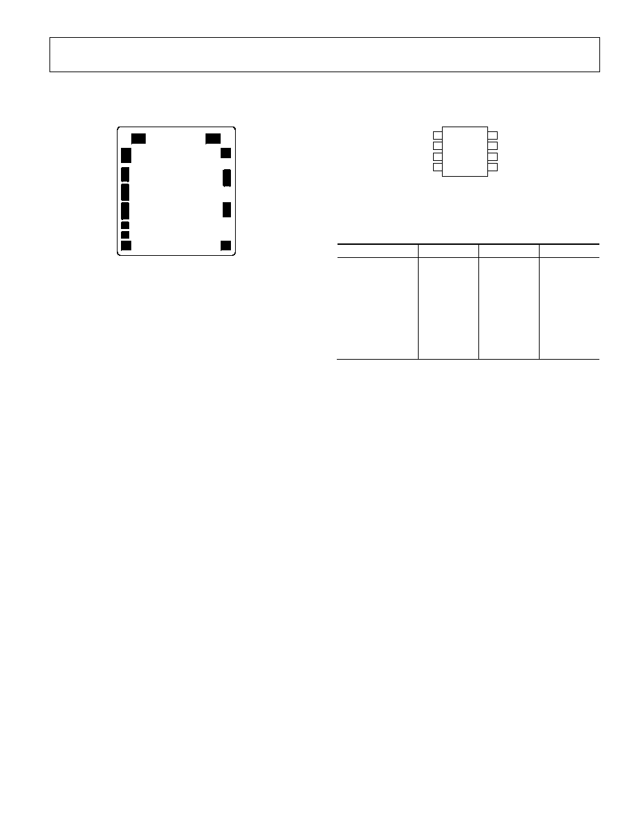
PIN CONFIGURATION AND FUNCTION DESCRIPTIONS
1
8
2
3
5
6
7
05147-011
Figure 2. Metallization Diagram
IN
1
GND
2
V
REF
2
3
NC
4
+IN
8
V
REF
1
7
V+
6
OUT
5
NC = NO CONNECT
AD8210
TOP VIEW
(Not to Scale)
05147-012
Figure 3. Pin Configuration
Table 3. Pin Function Descriptions
Pin No.
Mnemonic
X
Y
1 -IN
2 GND
3 V
REF
2
4 NC
5 OUT
6 V+
7 V
REF
1
8 +IN
AD8210
Preliminary Technical Data
Rev. PrB | Page 6 of 12
TYPICAL PERFORMANCE CHARACTERISTICS
Figure 4. Typical Offset Drift
Figure 5. CMR vs. Frequency
Figure 6. Gain Drift
Figure 7. Typical Small Signal Bandwidth (V
OUT
= 200 mV p-p)
Figure 8. Quiescent Current vs. Common-Mode Voltage
Figure 9. Differential Overload Recovery (Falling)

Preliminary Technical Data
AD8210
Rev. PrB | Page 7 of 12
Figure 10. Gain Drift
Figure 11. Settling Time
Figure 12. Quiescent Current vs. Output Voltage
Figure 13. Common-Mode Response
Figure 14. Rise/Fall Time
Figure 15. Input Common-Mode Range vs. Supply
AD8210
Preliminary Technical Data
Rev. PrB | Page 8 of 12
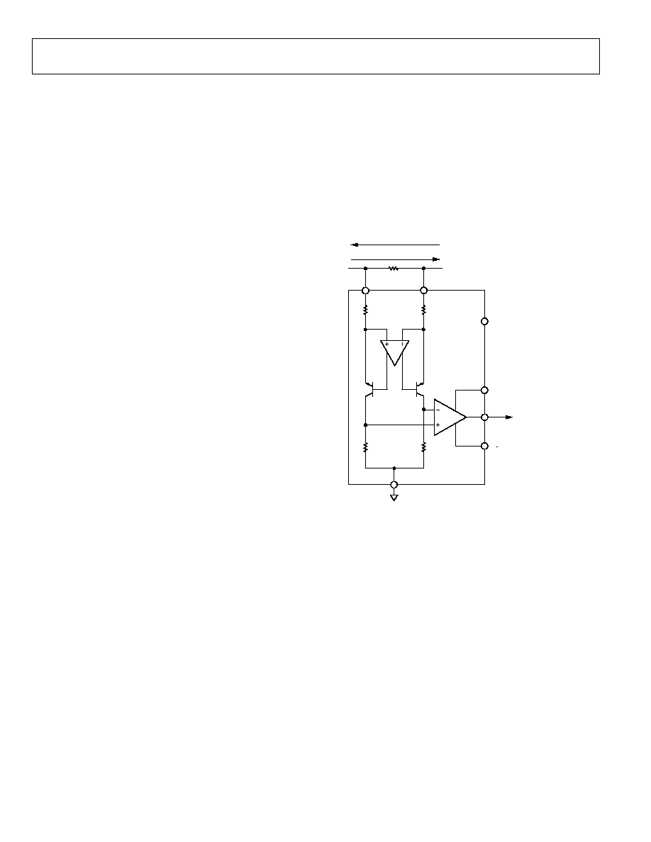
THEORY OF OPERATION
The AD8210 is a single-supply current shunt amplifier that uses
a unique architecture to accurately amplify small differential
current shunt voltages in the presence of rapidly changing
common-mode voltages. It is offered in both packaged and die
form.
In typical applications, the AD8210 is used to measure current
by amplifying the voltage across a current shunt placed across
the inputs.
The gain of the AD8210 is 20 V/V, with an accuracy of 1.5%.
This accuracy is guaranteed over the operating temperature
range of -40°C to +125°C. The die temperature range is -40°C
to +150°C with a guaranteed gain accuracy of 2.5%.
The AD8210 operates with a single supply from 4.5 V to 5.5V
(absolute maximum = 12.5 V). The supply current is typically
less than 1 mA.
The AD8210 is comprised of two main blocks, a differential and
an instrumentation amplifier. A load current flowing through
the external shunt resistor produces a voltage at the input ter-
minals of the AD8210. The input terminals are connected to the
differential amplifier (A1) by Resistors R1 and R2. A1 nulls the
voltage appearing across its own input terminals by adjusting
the current through R1 and R2 with Transistors Q1 and Q2.
When the input signal to the AD8210 is 0, the currents in R1
and R2 are equal. When the differential signal is nonzero, the
current increases through one of the resistors and decreases in
the other. The current difference is proportional to the size and
polarity of the input signal. Since the differential input voltage is
converted into a current, common-mode rejection is no longer
reliant on resistor matching, and high accuracy and perform-
ance is provided throughout the wide common-mode voltage
range.
The differential currents through QI and Q2 are converted into
a differential voltage due to R3 and R4. A2 is configured as an
instrumentation amplifier, and this differential input signal is
converted into a single-ended output voltage by A2. The gain is
internally set with thin-film resistors to 20V/V.
The output reference voltage is easily programmed by the V
REF
1
and V
REF
2 pins. In a typical configuration, V
REF
1 is connected to
V
CC
while V
REF
2 to GND. In this case, the output is centered at
V
CC
/2 when the input signal is 0.
I
SHUNT
R
SHUNT
AD8210
V
OUT
= (I
SHUNT
×
R
SHUNT
)
×
20
A2
R1
R2
V
S
V
REF
1
V
REF
2
GND
05147-010
A1
R3
R4
Q1
Q2
Figure 16. Simplified Schematic
Preliminary Technical Data
AD8210
Rev. PrB | Page 9 of 12
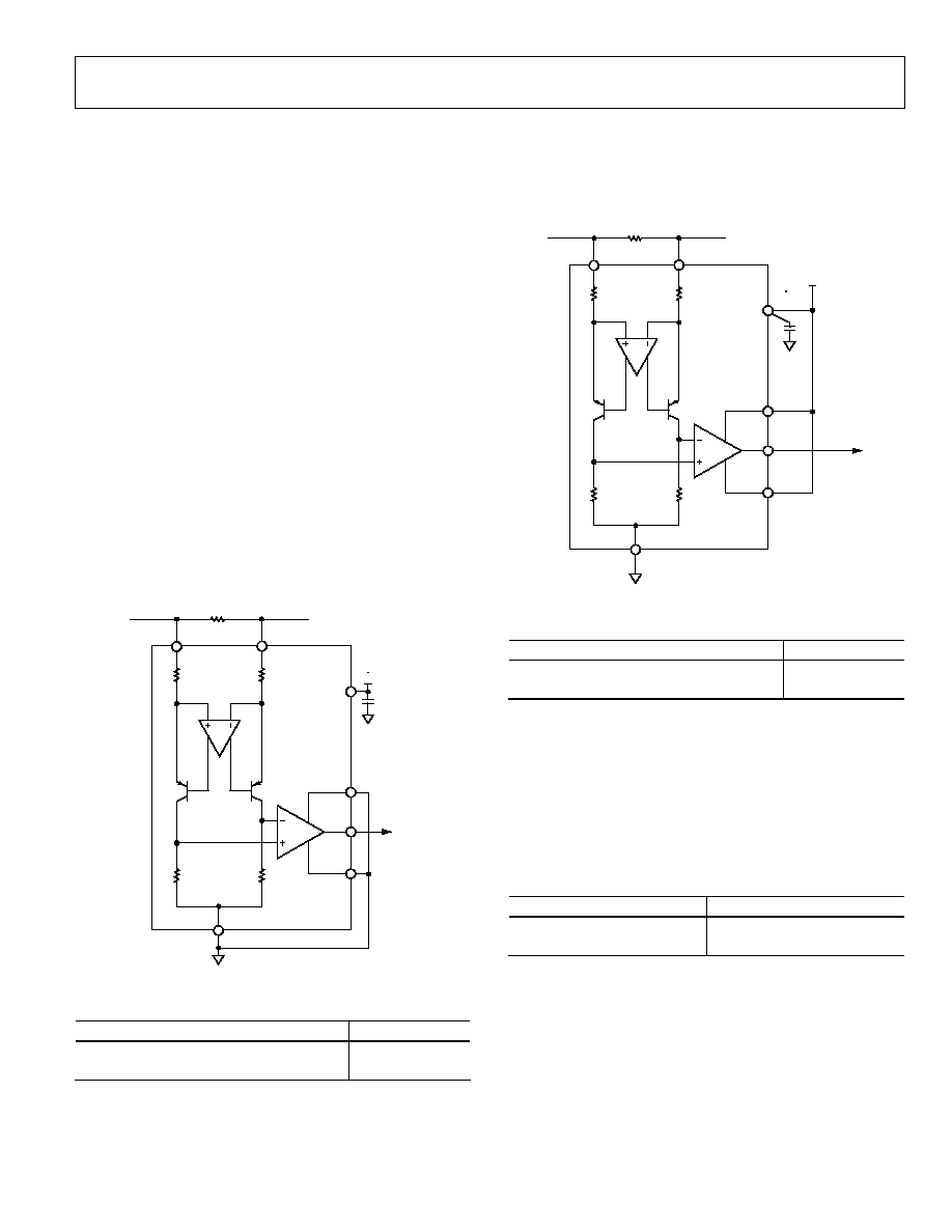
OUTPUT OFFSET ADJUSTMENT
The output of the AD8210 can be adjusted for unidirectional or
bidirectional operation.
UNIDIRECTIONAL OPERATION
Unidirectional operation allows the AD8210 to measure
currents through a resistive shunt in one direction. The basic
modes for unidirectional operation are ground-referenced
output mode and V+ referenced output mode.
With unidirectional operation, the output can be set at the
negative rail (near ground) or at positive rail (near V+) when
the differential input is 0 V. The output moves to the opposite
rail when a correct polarity differential input voltage is applied.
In this case, full scale is approximately 250 mV. The required
polarity of the differential input depends on the output voltage
setting. If the output is set at the positive rail, the input polarity
needs to be negative to move the output down. If the output is
set at ground, the polarity is positive to move the output up.
GROUND REFERENCED OUTPUT
When using the AD8210 in this mode, both reference inputs
are tied to ground, which causes the output to sit at the negative
rail when there are zero differential volts at the input (see
Figure 17).
AD8210
OUTPUT
G = +20
R
S
+IN
IN
V
S
V
REF
1
V
REF
2
GND
05147-002
0.1
µ
F
Figure 17. Ground Referenced Output
Table 4. V+ = 5 V
V
IN
(Referred to -IN)
V
O
0 V
0.05 V
250 mV
4.8 V
V+ REFERENCED OUTPUT
This mode is set when both reference pins are tied to the
positive supply. It is typically used when the diagnostic scheme
requires detection of the amplifier and the wiring before power
is applied to the load (see Figure 18).
AD8210
OUTPUT
G = +20
R
S
+IN
IN
V
S
V
REF
1
V
REF
2
GND
0.1
µ
F
05147-003
Figure 18. V+ Referenced Output
Table 5. V+ = 5 V
V
IN
(Referred to -IN)
V
O
0 V
4.8 V
250 mV
0.05 V
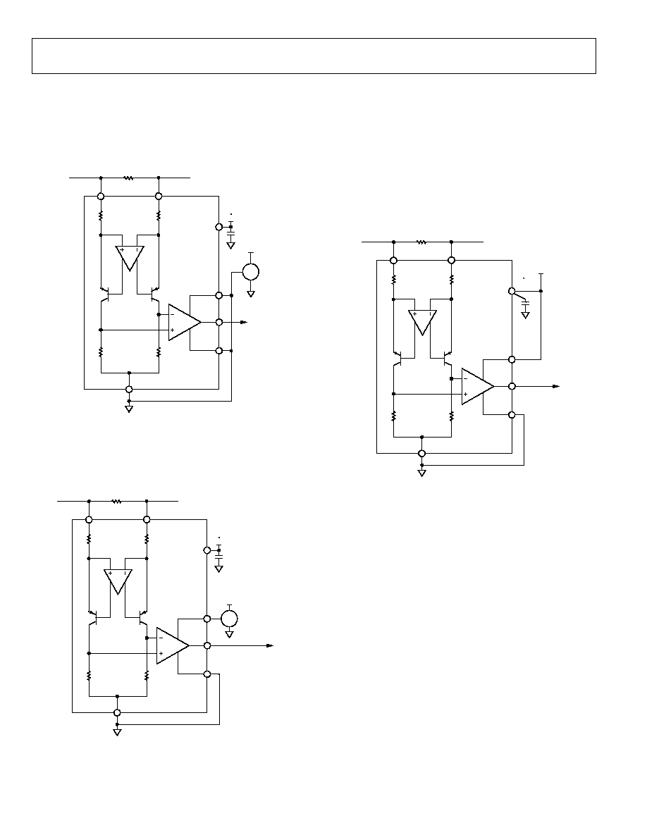
BIDIRECTIONAL OPERATION
Bidirectional operation allows the AD8210 to measure currents
through a resistive shunt in two directions.
In this case, the output is set anywhere within the output range.
Typically, it is set at half-scale for equal range in both directions.
In some cases, however, it is set at a voltage other than half-scale
when the bidirectional current is nonsymmetrical.
Table 6. V+ = 5 V, V
O
= 2.5 with V
IN
= 0 V
V
IN
(Referred to -IN)
V
O
+100 mV
4.5 V
-100 mV
0.5 V
Adjusting the output is accomplished by applying voltage(s) to
the reference inputs.
Pins V
REF
1 and V
REF
2 are tied to internal resistors that connect to
an internal offset node. There is no operational difference be-
tween the pins.
AD8210
Preliminary Technical Data
Rev. PrB | Page 10 of 12
EXTERNAL REFERENCE OUTPUT
Tying both pins together and to a reference produces an output
at the reference voltage when there is no differential input (see
Figure 19). The output moves down from the reference voltage
when the input is negative relative to the -IN pin and up when
the input is positive relative to the -IN pin.
AD8210
OUTPUT
G = +20
R
S
+IN
IN
V
S
V
REF
1
V
REF
2
GND
2.5V
05147-004
0.1
µ
F
Figure 19. External Reference Output
SPLITTING AN EXTERNAL REFERENCE
In this case, an external reference is divided by 2 with an
accuracy of approximately 0.5% by connecting one V
REF
pin to
ground and the other V
REF
pin to the reference (see Figure 20).
5V
AD8210
OUTPUT
G = +20
R
S
+IN
IN
V
S
V
REF
1
V
REF
2
GND
05147-005
0.1
µ
F
Figure 20. Split External Reference
SPLITTING THE SUPPLY
By tying one reference pin to V+ and the other to the GND
pin, the output is set at half of the supply when there is no
differential input (see Figure 21). The benefit is that no external
reference is required to offset the output for bidirectional
current measurement. This creates a midscale offset that is
ratiometric to the supply, which means that if the supply
increases or decreases, the output remains at half the supply.
For example, if the supply is 5.0 V, the output is at half scale or
2.5 V. If the supply increases by 10% (to 5.5 V), the output goes
to 2.75 V.
0.1
µ
F
AD8210
OUTPUT
G = +20
R
S
+IN
IN
V
S
V
REF
1
V
REF
2
GND
05147-006
Figure 21. Split Supply
Preliminary Technical Data
AD8210
Rev. PrB | Page 11 of 12
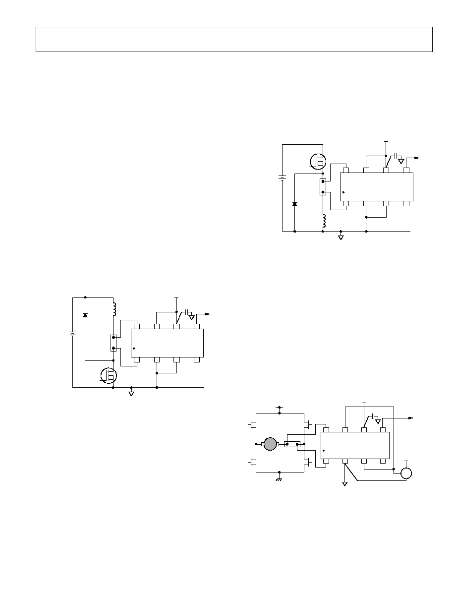
APPLICATIONS
A typical application for the AD8210 is high-side measurement
of a current through a solenoid for PWM control of the sole-
noid opening. Typical applications include hydraulic transmis-
sion control and diesel injection control.
Two typical circuit configurations are used for this type of ap-
plication.
HIGH-SIDE CURRENT SENSE WITH A LOW-SIDE
SWITCH
In this case, the PWM control switch is ground referenced. An
inductive load (solenoid) is tied to a power supply. A resistive
shunt is placed between the switch and the load (see Figure 22).
An advantage of placing the shunt on the high side is that the
entire current, including the recirculation current, can be meas-
ured since the shunt remains in the loop when the switch is off.
In addition, diagnostics can be enhanced because shorts to
ground can be detected with the shunt on the high side.
In this circuit configuration, when the switch is closed, the
common-mode voltage moves down to near the negative rail.
When the switch is opened, the voltage reversal across the in-
ductive load causes the common-mode voltage to be held one
diode drop above the battery by the clamp diode.
05147-007
INDUCTIVE
LOAD
CLAMP
DIODE
42V
BATTERY
SHUNT
SWITCH
NC = NO CONNECT
5V
+IN
V
REF
1
+V
S
OUT
IN
GND
V
REF
2
NC
AD8210
0.1
µ
F
Figure 22. Low-Side Switch
HIGH-SIDE CURRENT SENSE WITH A HIGH-SIDE
SWITCH
This configuration minimizes the possibility of unexpected
solenoid activation and excessive corrosion (see Figure 23). In
this case, both the switch and the shunt are on the high side.
When the switch is off, this removes the battery from the load,
which prevents damage from potential shorts to ground, while
still allowing the recirculation current to be measured and pro-
viding for diagnostics. Removing the power supply from the
load for the majority of the time minimizes the corrosive effects
that could be caused by the differential voltage between the load
and ground.
When using a high-side switch, the battery voltage is connected
to the load when the switch is closed, causing the common-
mode voltage to increase to the battery voltage. In this case,
when the switch is opened, the voltage reversal across the
inductive load causes the common-mode voltage to be held one
diode drop below ground by the clamp diode.
05147-008
INDUCTIVE
LOAD
CLAMP
DIODE
42V
BATTERY
SHUNT
SWITCH
NC = NO CONNECT
5V
+IN
V
REF
1
+V
S
OUT
IN
GND
V
REF
2
NC
AD8210
0.1
µ
F
Figure 23. High-Side Switch
Another typical application for the AD8210 is as part of the
control loop in H-bridge motor control. In this case, the
AD8210 is placed in the middle of the H-bridge (see Figure 24)
so that it can accurately measure current in both directions by
using the shunt available at the motor. This is a better solution
than a ground referenced op amp because ground is not typi-
cally a stable reference voltage in this type of application. This
instability in the ground reference causes the measurements
that could be made with a simple ground referenced op amp to
be inaccurate.
The AD8210 measures current in both directions as the H-
bridge switches and the motor changes direction. The output of
the AD8210 is configured in an external reference bidirectional
mode, see the Output Offset Adjustment.
05147-009
SHUNT
2.5V
5V
CONTROLLER
NC = NO CONNECT
MOTOR
5V
+IN
V
REF
1
+V
S
OUT
IN
GND
V
REF
2
NC
AD8210
0.1
µ
F
Figure 24. Motor Control Application
AD8210
Preliminary Technical Data
Rev. PrB | Page 12 of 12
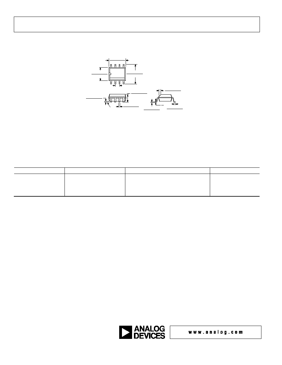
OUTLINE DIMENSIONS
0.25 (0.0098)
0.17 (0.0067)
1.27 (0.0500)
0.40 (0.0157)
0.50 (0.0196)
0.25 (0.0099)
×
45°
8°
0°
1.75 (0.0688)
1.35 (0.0532)
SEATING
PLANE
0.25 (0.0098)
0.10 (0.0040)
4
1
8
5
5.00 (0.1968)
4.80 (0.1890)
4.00 (0.1574)
3.80 (0.1497)
1.27 (0.0500)
BSC
6.20 (0.2440)
5.80 (0.2284)
0.51 (0.0201)
0.31 (0.0122)
COPLANARITY
0.10
CONTROLLING DIMENSIONS ARE IN MILLIMETERS; INCH DIMENSIONS
(IN PARENTHESES) ARE ROUNDED-OFF MILLIMETER EQUIVALENTS FOR
REFERENCE ONLY AND ARE NOT APPROPRIATE FOR USE IN DESIGN
COMPLIANT TO JEDEC STANDARDS MS-012AA
Figure 25. 8-Lead Standard Small Outline Package [SOIC]
Narrow Body
(R-8)
Dimensions shown in millimeters and (inches)
ORDERING GUIDE
Model
Temperature Range
Package Description
Package Option
AD8210YR
-40°C to +125°C
8-Lead SOIC
R-8
AD8210YR-REEL
-40°C to +125°C
8-Lead SOIC, 13" Tape and Reel
R-8
AD8210YR-REEL7
-40°C to +125°C
8-Lead SOIC, 7" Tape and Reel
R-8
AD8210YCSURF
-40°C to +150°C
Die Form
© 2005 Analog Devices, Inc. All rights reserved. Trademarks and
registered trademarks are the property of their respective owners.
PR0514701/05(PrB)
Document Outline
- FEATURES
- EXCELLENT AC AND DC PERFORMANCE
- APPLICATIONS
- TYPICAL OPERATING CIRCUIT
- GENERAL DESCRIPTION
- TABLE OF CONTENTS
- þÿ
- þÿ
- þÿ
- þÿ
- þÿ
- þÿ
- þÿ
- þÿ