 | –≠–ª–µ–∫—Ç—Ä–æ–Ω–Ω—ã–π –∫–æ–º–ø–æ–Ω–µ–Ω—Ç: AD8312 | –°–∫–∞—á–∞—Ç—å:  PDF PDF  ZIP ZIP |
100 MHz-2.7 GHz, 45 dB
RF Log Detector
Preliminary Technical Data
AD8312
PrA
10/29/2004
Information furnished by Analog Devices is believed to be accurate and reliable.
However, no responsibility is assumed by Analog Devices for its use, nor for any
infringements of patents or other rights of third parties that may result from its use.
Specifications subject to change without notice. No license is granted by implication
or otherwise under any patent or patent rights of Analog Devices. Trademarks and
registered trademarks are the property of their respective owners.
One Technology Way, P.O. Box 9106, Norwood, MA 02062-9106, U.S.A.
Tel: 781.329.4700
www.analog.com
Fax: 781.326.8703
© 2004 Analog Devices, Inc. All rights reserved.
FEATURES
Complete RF Detector Function
Typical Range : -45 dBm to 0 dBm re 50
Frequency Response from 100 MHz to 2.7 GHz
Temperature-Stable Linear-in-dB Response
Accurate to 2.7 GHz
Rapid Response: 70 ns to a 10 dB Step
Low Power: 12 mW at 2.7 V
APPLICATIONS
Cellular Handsets (GSM, CDMA, WCDMA)
RSSI and TSSI for Wireless Terminal Devices
Transmitter Power Measurement
PRODUCT DESCRIPTION
The AD8312 is a complete low cost subsystem for the
measurement of RF signals in the frequency range of 100 MHz
to 2.7 GHz, with a typical dynamic range of 45 dB, intended for
use in a wide variety of cellular handsets and other wireless
devices. It provides a wider dynamic range and better accuracy
than possible using discrete diode detectors. In particular, its
temperature stability is excellent over the full operating range of
-40∞C to +85∞C.
Its high sensitivity allows measurement at low power levels, thus
reducing the amount of power that needs to be coupled to the
detector. It is essentially a voltage-responding device, with a
typical signal range of 1.25 mV to 224 mV rms or -45 dBm to 0
dBm re 50 .
For convenience, the signal is internally ac-coupled, using a 5
pF capacitor to a load of 3 k in shunt with 2 pF. This high-
pass coupling, with a corner at approximately 16 MHz,
determines the lowest operating frequency. Thus, the source
may be dc-grounded.
The AD8312 output, called VOUT, increases from close to
ground to about 1.2 V as the input signal level increases from
1.25 mV to 224 mV. This output is intended for use in
measurement mode. Consult the Applications section of this
data sheet for information on use in this mode. A capacitor may
be connected between the VOUT and CFLT pins when it is
desirable to increase the time interval over which averaging of
the input waveform occurs.
The AD8312 is available in a 6-lead wafer-level chip scale
package, 1.0 mm x 1.5 mm, and consumes 4.5 mA from a 2.7 V
to 5.5 V supply.
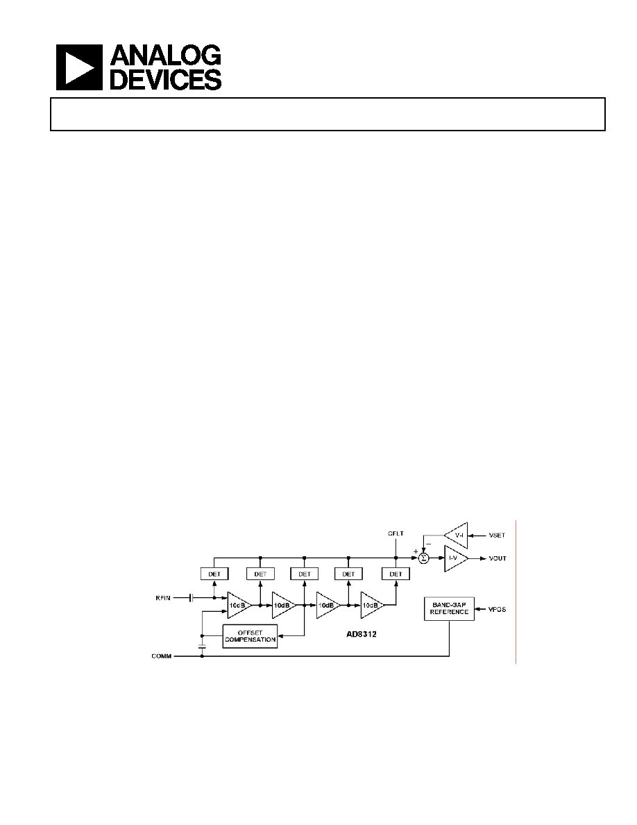
FUNCTIONAL BLOCK DIAGRAM
Figure 1.

AD8312
Preliminary Technical Data
Rev. PrA| Page 2 of 13
TABLE OF CONTENTS
Specifications..................................................................................... 3
Absolute Maximum Ratings............................................................ 5
ESD Caution.................................................................................. 5
Pin Configuration and Function Descriptions............................. 6
Typical Performance Characteristics ............................................. 7
General Description ....................................................................... 10
Applications..................................................................................... 11
Basic Connections...................................................................... 11
Evaluation Board ........................................................................ 11
Outline Dimensions ....................................................................... 13
Ordering Guide .......................................................................... 13

Preliminary Technical Data
AD8312
Rev. PrA| Page 3 of 13
SPECIFICATIONS
Table 1. V
S
= 3 V, C
FLT
= open, T
A
= 25∞C, 52.3 termination resistor at RFIN, unless otherwise noted.
Parameter
Conditions
Min
Typ
Max
Unit
SIGNAL INPUT INTERFACE
RFIN (Pin 6)
Specified Frequency Range
0.1
2.7
GHz
Input Voltage Range
Internally AC-Coupled
1.25
224
mV rms
Equivalent Power Range
52.3 External Termination
≠45
0
dBm
DC Resistance to COMM
100
k
MEASUREMENT MODE
VOUT (Pin 2) shorted to VSET (Pin 3), Sinusoidal
Input Signal
f = 0.1 GHz
Input Impedance
3020 || 1.35
|| pF
± 1 dB Dynamic Range
T
A
= +25
∞C
48
dB
-40
∞C < T
A
< +85
∞C
40
dB
Maximum Input Level
± 1 dB Error
2
dBm
Minimum Input Level
± 1 dB Error
-46
dBm
Slope
21.0
mV/dB
Intercept
-50.4
dBm
Output Voltage - High Power In
P
IN
= ≠10 dBm
0.85
V
Output Voltage - Low Power In
P
IN
= ≠40 dBm
0.22
V
Temperature Sensitivity
P
IN
= ≠10 dBm
25
∞C T
A
+85∞C
-
0.0002
dB/
∞C
-40
∞C T
A
+25∞C
-
0.0050
dB/
∞C
f = 0.9 GHz
Input Impedance
903 || 1.16
|| pF
± 1 dB Dynamic Range
T
A
= +25
∞C
50
dB
-40
∞C < T
A
< +85
∞C
40
dB
Maximum Input Level
± 1 dB Error
2
dBm
Minimum Input Level
± 1 dB Error
-48
dBm
Slope
20.3
mV/dB
Intercept
-51.4
dBm
Output Voltage - High Power In
P
IN
= ≠10 dBm
0.839
V
Output Voltage - Low Power In
P
IN
= ≠40 dBm
0.226
V
Temperature Sensitivity
P
IN
= ≠10 dBm
25
∞C T
A
+85∞C
-
0.0036
dB/
∞C
≠40
∞C T
A
+25∞C
-0.0010
dB/
∞C
f = 1.9 GHz
Input Impedance
440 || 1.14
|| pF
± 1 dB Dynamic Range
T
A
= +25
∞C
46
dB
-40
∞C < T
A
< +85
∞C
38
dB
Maximum Input Level
± 1 dB Error
-3
dBm
Minimum Input Level
± 1 dB Error
-49
dBm
Slope
19.4
mV/dB
Intercept
-51.8
dBm
Output Voltage - High Power In
P
IN
= ≠10 dBm
0.815
V
Output Voltage - Low Power In
P
IN
= ≠40 dBm
0.229
V
Temperature Sensitivity
P
IN
= ≠10 dBm
25
∞C T
A
+85∞C
-0.0044
dB/
∞C
≠40
∞C T
A
+25∞C
-0.0027
dB/
∞C
AD8312
Preliminary Technical Data
Rev. PrA| Page 4 of 13
Parameter
Conditions
Min
Typ
Max
Unit
f = 2.5 GHz
Input Impedance
365 || 1.1
|| pF
± 1 dB Dynamic Range
T
A
= +25
∞C
44
dB
-40
∞C < T
A
< +85
∞C
36
dB
Maximum Input Level
± 1 dB Error
-4
dBm
Minimum Input Level
± 1 dB Error
-48
dBm
Slope
18.85
mV/dB
Intercept
-51
dBm
Output Voltage - High Power In
P
IN
= ≠10 dBm
0.774
V
Output Voltage - Low Power In
P
IN
= ≠40 dBm
0.205
V
Temperature Sensitivity
P
IN
= ≠10 dBm
25
∞C T
A
+85∞C
+0.0053 dB/
∞C
≠40
∞C T
A
+25∞C
-0.0047 dB/
∞C
OUTPUT INTERFACE
VOUT (Pin 2)
Minimum Output Voltage
No Signal at RFIN, R
L
10 k
0.02
V
Maximum Output Voltage
1
R
L
10 k
2.2
V
General Limit
2.7 V V
S
5.5 V
V
S
≠ 1
V
Available Output Current
Sourcing/Sinking
2/1
mA
Residual RF (at 2f)
f = 0.1 GHz (Worst Condition)
100
µV
Output Noise
RF Input = 2.2 GHz, ≠10 dBm, f
NOISE
= 100 kHz,
CFLT open
tbd
uV/
Hz
Fall Time
Input Level = off to 0 dBm, 90% to 10%
120
ns
Rise Time
Input Level = 0 dBm to off, 10% to 90%
85
ns
VSET INTERFACE
VSET (Pin 3)
Input Resistance
10
k
Bias Current Source
RFIN = -10 dBm; VSET = 1.2V
tbd
µA
POWER INTERFACE
VPOS (Pin 1)
Supply Voltage
2.7
3.0
5.5
V
Quiescent Current
4.2
mA
vs. Temperature
≠40
∞C T
A
+85∞C
4.3
mA
1
Increased output possible when using an attenuator between VOUT and VSET to raise the slope.
Preliminary Technical Data
AD8312
Rev. PrA| Page 5 of 13
ABSOLUTE MAXIMUM RATINGS
Table 2.
Parameter Value
Supply Voltage VPOS
5.5 V
VOUT, VSET
0 V, VPOS
Input Voltage
1.6 V rms
Equivalent Power
+17 dBm
Internal Power Dissipation
TBD mW
JA
(WLCSP)
TBD
∞C/W
Maximum Junction Temperature
125
∞C
Operating Temperature Range
≠40
∞C to +85∞C
Storage Temperature Range
≠65
∞C to +150∞C
Lead Temperature Range (Soldering 60 sec)
260
∞C
Stresses above those listed under Absolute Maximum Ratings
may cause permanent damage to the device. This is a stress
rating only; functional operation of the device at these or any
other conditions above those indicated in the operational
section of this specification is not implied. Exposure to absolute
maximum rating conditions for extended periods may affect
device reliability.
ESD CAUTION
ESD (electrostatic discharge) sensitive device. Electrostatic charges as high as 4000 V readily accumulate on
the human body and test equipment and can discharge without detection. Although this product features
proprietary ESD protection circuitry, permanent damage may occur on devices subjected to high energy
electrostatic discharges. Therefore, proper ESD precautions are recommended to avoid performance
degradation or loss of functionality.
AD8312
Preliminary Technical Data
Rev. PrA| Page 6 of 13
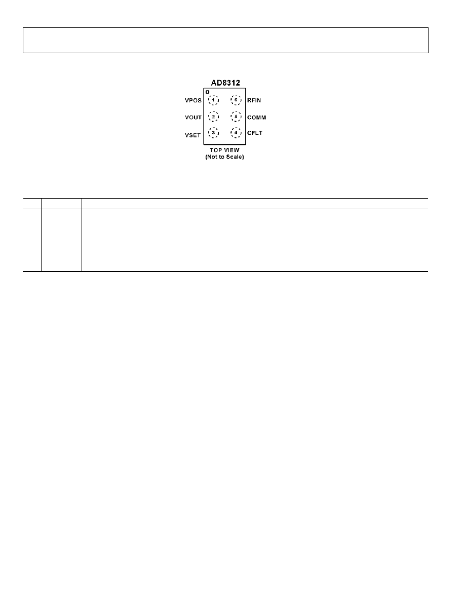
PIN CONFIGURATION AND FUNCTION DESCRIPTIONS
Figure 2. Pin Configuration
Table 3. Pin Function Descriptions
Pin Mnemonic Function
1
VPOS
Positive supply voltage (V
S
), 2.7 V to 5.5 V.
2
VOUT
Logarithmic output. Output voltage increases with increasing input amplitude.
3
VSET
Setpoint input. Connect VSET to VOUT for measurement-mode operation.
4
CFLT
Connection for an external capacitor to slow the response of the output. Capacitor is connected between CFLT and
VOUT.
5
COMM
Device Common (Ground)
6
RFIN
RF Input
Preliminary Technical Data
AD8312
Rev. PrA| Page 7 of 13
TYPICAL PERFORMANCE CHARACTERISTICS
Figure 3. VOUT and Log Conformance vs. Input Amplitude at 50 MHz;
-40∞C, +25∞C, and +85∞C
0
0.1
0.2
0.3
0.4
0.5
0.6
0.7
0.8
0.9
1
1.1
1.2
1.3
1.4
-65
-55
-45
-35
-25
-15
-5
5
P
IN
-dBm
Vo
u
t
- Vo
l
t
s
-2.8
-2.4
-2
-1.6
-1.2
-0.8
-0.4
0
0.4
0.8
1.2
1.6
2
2.4
2.8
E
r
ro
r -
d
B
Figure 4. VOUT and Log Conformance vs. Input Amplitude at 100 MHz;
-40∞C, +25∞C, and +85∞C
0
0.1
0.2
0.3
0.4
0.5
0.6
0.7
0.8
0.9
1
1.1
1.2
1.3
1.4
-65
-55
-45
-35
-25
-15
-5
5
P
IN
-dBm
Vo
u
t
- Vo
l
t
s
-2.8
-2.4
-2
-1.6
-1.2
-0.8
-0.4
0
0.4
0.8
1.2
1.6
2
2.4
2.8
E
r
ro
r -
d
B
Figure 5. VOUT and Log Conformance vs. Input Amplitude at 900 MHz;
-40∞C, +25∞C, and +85∞C
0
0.1
0.2
0.3
0.4
0.5
0.6
0.7
0.8
0.9
1
1.1
1.2
1.3
1.4
-65
-55
-45
-35
-25
-15
-5
5
P
IN
-dBm
Vo
u
t
- Vo
l
t
s
-2.8
-2.4
-2
-1.6
-1.2
-0.8
-0.4
0
0.4
0.8
1.2
1.6
2
2.4
2.8
E
r
ro
r -
d
B
Figure 6. VOUT and Log Conformance vs. Input Amplitude at 1.9 GHz;
-40∞C, +25∞C, and +85∞C
Figure 7. VOUT and Log Conformance vs. Input Amplitude at 2.2 GHz;
-40∞C, +25∞C, and +85∞C
0
0.1
0.2
0.3
0.4
0.5
0.6
0.7
0.8
0.9
1
1.1
1.2
1.3
1.4
-65
-55
-45
-35
-25
-15
-5
5
P
IN
-dBm
V
out -
V
o
l
t
s
-2.8
-2.4
-2
-1.6
-1.2
-0.8
-0.4
0
0.4
0.8
1.2
1.6
2
2.4
2.8
Er
ro
r
-
d
B
Figure 8. VOUT and Log Conformance vs. Input Amplitude at 2.5 GHz;
-40∞C, +25∞C, and +85∞C
AD8312
Preliminary Technical Data
Rev. PrA| Page 8 of 13
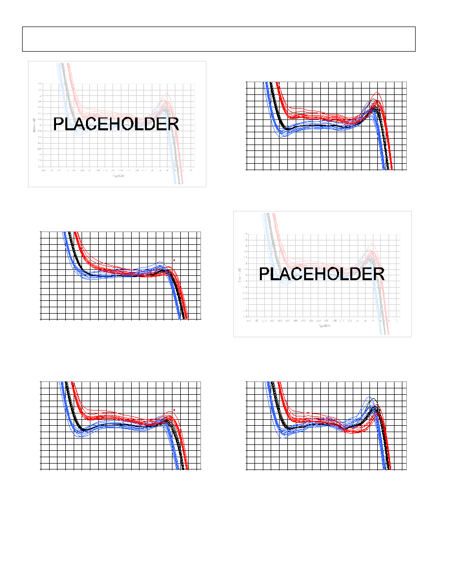
Figure 9. Distribution of Error over Temperature after Ambient Normalization
vs. Input Amplitude at 50 MHz
-2.8
-2.4
-2
-1.6
-1.2
-0.8
-0.4
0
0.4
0.8
1.2
1.6
2
2.4
2.8
-64
-60
-56
-52
-48
-44
-40
-36
-32
-28
-24
-20
-16
-12
-8
-4
0
4
8
12
P
IN
-dBm
E
rror -
d
B
Figure 10. Distribution of Error over Temperature after Ambient Normalization
vs. Input Amplitude at 100 MHz
-2.8
-2.4
-2
-1.6
-1.2
-0.8
-0.4
0
0.4
0.8
1.2
1.6
2
2.4
2.8
-64
-60
-56
-52
-48
-44
-40
-36
-32
-28
-24
-20
-16
-12
-8
-4
0
4
8
12
P
IN
-dBm
E
rror -
d
B
Figure 11. Distribution of Error over Temperature after Ambient Normalization
vs. Input Amplitude at 900 MHz
-2.8
-2.4
-2
-1.6
-1.2
-0.8
-0.4
0
0.4
0.8
1.2
1.6
2
2.4
2.8
-64
-60
-56
-52
-48
-44
-40
-36
-32
-28
-24
-20
-16
-12
-8
-4
0
4
8
12
P
IN
-dBm
E
rro
r -
dB
Figure 12. Distribution of Error over Temperature after Ambient Normalization
vs. Input Amplitude at 1.9 GHz
Figure 13. Distribution of Error over Temperature after Ambient Normalization
vs. Input Amplitude at 2.2 GHz
-2.8
-2.4
-2
-1.6
-1.2
-0.8
-0.4
0
0.4
0.8
1.2
1.6
2
2.4
2.8
-64
-60
-56
-52
-48
-44
-40
-36
-32
-28
-24
-20
-16
-12
-8
-4
0
4
8
12
P
IN
-dBm
E
rror -
d
B
Figure 14. Distribution of Error over Temperature after Ambient Normalization
vs. Input Amplitude at 2.5 GHz
Preliminary Technical Data
AD8312
Rev. PrA| Page 9 of 13
Figure 15. VOUT Response Time, RF Off to 0 dBm
Figure 16. Test Setup for Pulse Response
Figure 17. Input Impedance vs. Frequency; No Termination Resistor on RFIN
Figure 18. Power-On and Power-Off Response
Figure 19. Test Setup for Power-On and Power-Off Response
Figure 20. Noise Spectral Density of Output; C
FLT
= Open
AD8312
Preliminary Technical Data
Rev. PrA| Page 10 of 13
GENERAL DESCRIPTION
The AD8312 is a logarithmic amplifier (log amp) similar in
design to the AD8313; further details about the structure and
function may be found in the AD8313 data sheet and other log
amps produced by Analog Devices. Figure 21 shows the main
features of the AD8312 in block schematic form.
The AD8312 combines two key functions needed for the
measurement of signal level over a moderately wide dynamic
range. First, it provides the amplification needed to respond to
small signals, in a chain of four amplifier/limiter cells, each
having a small-signal gain of 10 dB and a bandwidth of
approximately 3.5 GHz. At the output of each of these amplifier
stages is a full-wave rectifier, essentially a square-law detector
cell, that converts the RF signal voltages to a fluctuating current
having an average value that increases with signal level. A
further passive detector stage is added ahead of the first stage.
Thus, there are five detectors, each separated by 10 dB,
spanning some 50 dB of dynamic range.
The output of these detector cells is in the form of a differential
current, making their summation a simple matter. It can easily
be shown that such summation closely approximates a
logarithmic function. This result is then converted to a voltage,
at pin VOUT, through a high-gain stage. In measurement
modes, this output is connected back to a voltage-to-current
(V≠I) stage, in such a manner that VOUT is a logarithmic
measure of the RF input voltage, with a slope and intercept
controlled by the design. For a fixed termination resistance at
the input of the AD8312, a given voltage corresponds to a
certain power level.
The external termination added ahead of the AD8312
determines the effective power scaling. This will often take the
form of a simple resistor (52.3 will provide a net 50 input)
but more elaborate matching networks may be used. This
impedance determines the logarithmic intercept, the input
power for which the output would cross the baseline (VOUT =
zero) if the function were continuous for all values of input.
Since this is never the case for a practical log amp, the intercept
refers to the value obtained by the minimum-error straight-line
fit to the actual graph of VOUT versus PIN. The quoted values
assume a sinusoidal (CW) signal. Where there is complex
modulation, as in CDMA, the calibration of the power response
needs to be adjusted accordingly. Where a true power
(waveform-independent) response is needed, the use of an rms-
responding detector, such as the AD8361, should be considered.
However, the logarithmic slope, the amount by which the
output VOUT changes for each decibel of input change (voltage
or power) is, in principle, independent of waveform or
termination impedance. In practice, it usually falls off
somewhat at higher frequencies, due to the declining gain of the
amplifier stages and other effects in the detector cells. For the
AD8312, the slope at low frequencies is nominally 21.3 mV/dB,
falling almost linearly with frequency to about 19.2 mV/dB at
2.5 GHz. These values are sensibly independent of temperature
and almost totally unaffected by the supply voltage from 2.7 V
to 5.5 V.
Figure 21. Block Schematic
Preliminary Technical Data
AD8312
Rev. PrA| Page 11 of 13
APPLICATIONS
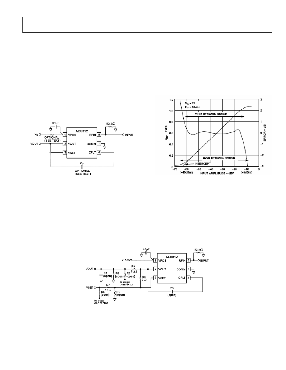
BASIC CONNECTIONS
Figure 22 shows connections for the basic measurement mode.
A supply voltage of 2.7 V to 5.5 V is required. The supply to the
VPOS pin should be decoupled with a low inductance 0.1 µF
surface mount ceramic capacitor. A series resistor of about 10
may be added; this resistor will slightly reduce the supply
voltage to the AD8312 (maximum current into the VPOS pin is
approximately 9 mA when VOUT is delivering 5 mA). Its use
should be avoided in applications where the power supply
voltage is very low (i.e., 2.7 V). A series inductor will provide
similar power supply filtering with minimal drop in supply
voltage.
Figure 22. Basic Connections for Operation in Measurement Mode
The AD8312 has an internal input coupling capacitor. This
eliminates the need for external ac-coupling. A broadband
input match is achieved in this example by connecting a
52.3 resistor between RFIN and ground. This resistance
combines with the internal input impedance of approximately
3 k to give an overall broadband input resistance of 50 .
The measurement mode is selected by connecting VSET to
VOUT, which establishes a feedback path and sets the
logarithmic slope to its nominal value. The peak voltage range
of the measurement extends from -45 dBm to 0 dBm at
0.9 GHz, and only slightly less at higher frequencies up to
2.5 GHz. At a slope of 21.5 mV/dB, this would amount to an
output span of 967 mV. Figure 23 shows the transfer function
for VOUT at a supply voltage of 3 V, and input frequency of 0.9
GHz.
The load resistance on VOUT should not be lower than 10
k in order that the full-scale output of 1 V can be generated
with the limited available current of 200 µA max. Figure 23
shows the logarithmic conformance under the same conditions.
Figure 23. VOUT and Log Conformance Error vs. Input Level vs. Input Level
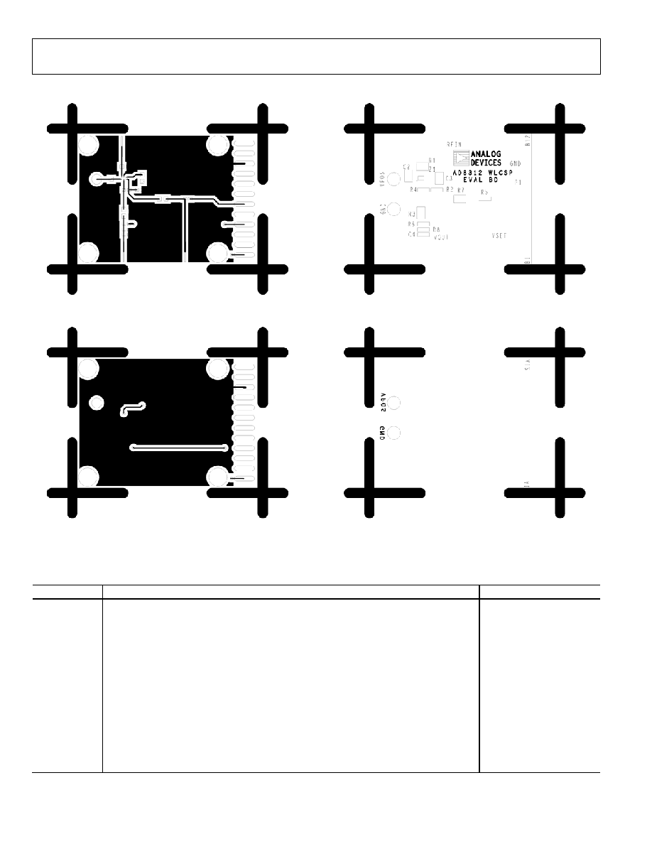
EVALUATION BOARD
Figure 24 shows the schematic of the AD8312 evaluation board.
The layout and silkscreen of the component and circuit sides
are shown in Figure 25 to Figure 28. The board is powered by a
single supply in the range, 2.7 V to 5.5 V. The power supply is
decoupled by a single 0.1 µF capacitor.
Table 4 details the various configuration options of the
evaluation board.
Figure 24. Evaluation Board Schematic
AD8312
Preliminary Technical Data
Rev. PrA| Page 12 of 13
Figure 25. Layout of Component Side (WLCSP)
Figure 26. Layout of Circuit Side (WLCSP))
Figure 27. Silkscreen of Component Side (WLCSP)
Figure 28. Silkscreen of Circuit Side (WLCSP)
Table 4. Evaluation Board Configuration Options
Component Function
Default Condition
VPOS, GND
Supply and Ground Vector Pins
Not Applicable
C2
Power Supply Decoupling: The nominal supply decoupling consists of a 0.1 µF capacitor
(C1).
C2 = 0.1 µF (Size 0603)
R1
Input Interface: The 52.3 resistor in position R1 combines with the AD8312's internal
input impedance to give a broadband input impedance of around 50 .
R1 = 52.3 (Size 0603)
R2, R4
Slope Adjust: By installing resistors in R2 and R4, the nominal slope of 20 mV/dB can be
changed. See Slope Adjust discussion for more details.
R2 = Open (Size 0402)
R4 = 0 (Size 0402)
C3
Filter Capacitor. The response time of VOUT can be modified by placing a capacitor
between CFLT (Pin 4) and VOUT.
C3 = Open (Size 0603)
R3, R8, C4
Output Interface: R3, R8, and C4 can be used to check the response of VOUT to capacitive
and resistive loading. R3/R8 can be used to attenuate VOUT.
R3 = 1k (Size 0603)
R8 = C4 = open (Size 0402)
R7
VSET Interface: R7 can be used to reduce capacitive loading from transmission lines.
R7 = 1k (Size 0603)
R5, R6
Alternate Interface: R5 and R6 allow for VOUT and VSET to be accessible from the edge
connector
R5 = R6 = Open (Size 0402)
Preliminary Technical Data
AD8312
Rev. PrA| Page 13 of 13
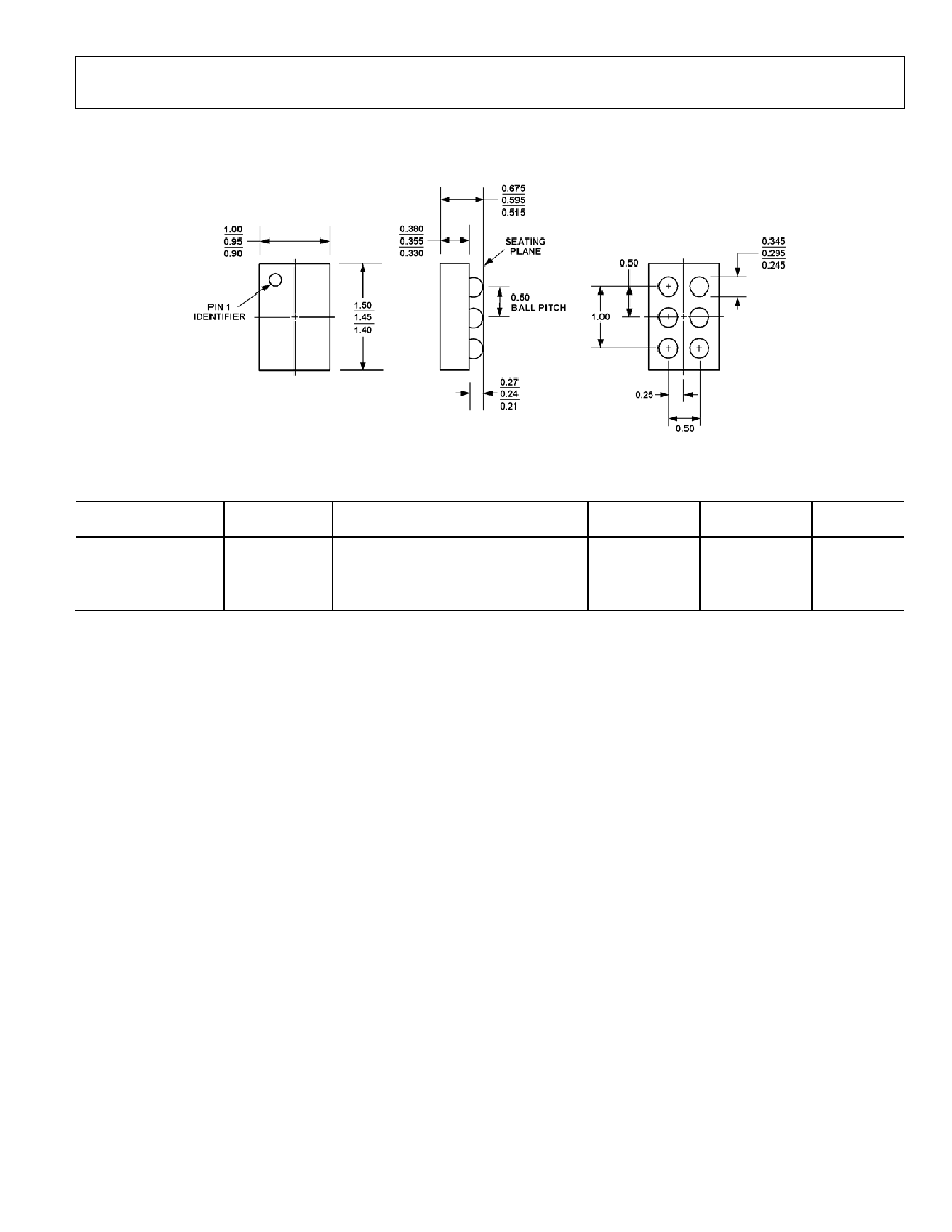
OUTLINE DIMENSIONS
Figure 29. Wafer-level Chip Scale Package
Dimensions shown in mm
ORDERING GUIDE
AD8312 Products
Temperature
Package
Package Description
Package
Outline
Branding
Information
Ordering
Quantity
AD8312ACPZ-REEL7
1
≠40∞C to +85∞C
6-Lead Wafer-level Chip Scale Package,
7" Tape and Reel
CB-6 Q00 tbd
AD8312ACPZ-WP
≠40∞C to +85∞C
6-Lead WLCSP, Waffle Pack
CB-6
Q00
tbd
AD8312-EVAL
Evaluation
Board
1
Z = Pb-free part.
PR05260-0-11/04(PrA)