Document Outline
- ˛ˇ
- ˛ˇ
- ˛ˇ
- ˛ˇ
- ˛ˇ
- ˛ˇ
- ˛ˇ
- ˛ˇ
- ˛ˇ
- ˛ˇ
- ˛ˇ
- ˛ˇ
- ˛ˇ
- ˛ˇ
- ˛ˇ
- ˛ˇ
- ˛ˇ
- ˛ˇ
- ˛ˇ
- ˛ˇ
- ˛ˇ
- ˛ˇ
- ˛ˇ
1 MHz to 10 GHz, 50 dB
Log Detector/Controller
AD8317
Rev. 0
Information furnished by Analog Devices is believed to be accurate and reliable. However, no
responsibility is assumed by Analog Devices for its use, nor for any infringements of patents or other
rights of third parties that may result from its use. Specifications subject to change without notice. No
license is granted by implication or otherwise under any patent or patent rights of Analog Devices.
Trademarks and registered trademarks are the property of their respective owners.
One Technology Way, P.O. Box 9106, Norwood, MA 02062-9106, U.S.A.
Tel: 781.329.4700
www.analog.com
Fax: 781.461.3113
© 2005 Analog Devices, Inc. All rights reserved.
FEATURES
Wide bandwidth: 1 MHz to 10 GHz
High accuracy: ±1.0 dB over temperature
50 dB dynamic range up to 8 GHz
Stability over temperature ±0.5 dB
Low noise measurement/controller output VOUT
Pulse response time: 8/10 ns (fall/rise)
Small footprint 2 mm x 3 mm CSP package
Supply operation: 3.0 V to 5.5 V @ 22 mA
Fabricated using high speed SiGe process
APPLICATIONS
RF transmitter PA setpoint control and level monitoring
Power monitoring in radiolink transmitters
RSSI measurement in base stations, WLAN, WiMAX, radar
GENERAL DESCRIPTION
The AD8317 is a demodulating logarithmic amplifier, capable
of accurately converting an RF input signal to a corresponding
decibel-scaled output. It employs the progressive compression
technique over a cascaded amplifier chain, each stage of which
is equipped with a detector cell. The device can be used in
either measurement or controller modes. The AD8317 maintains
accurate log conformance for signals of 1 MHz to 8 GHz and
provides useful operation to 10 GHz. The input dynamic range
is typically 50 dB (re: 50 ) with error less than ±1 dB. The AD8317
has 8/10 ns response time (fall time/rise time) that enables RF
burst detection to a pulse rate of beyond 50 MHz. The device
provides unprecedented logarithmic intercept stability vs. ambient
temperature conditions. A supply of 3.0 V to 5.5 V is required to
power the device. Current consumption is typically 22 mA, and it
decreases to 200 A when the device is disabled.
The AD8317 can be configured to provide a control voltage to
a power amplifier or a measurement output from the VOUT
pin. Because the output can be used for controller applications,
special
attention has been paid to minimize wideband noise. In this
mode, the setpoint control voltage is applied to the VSET pin.
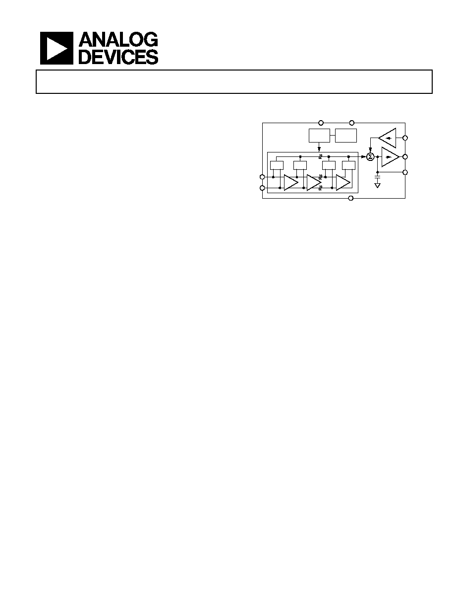
FUNCTIONAL BLOCK DIAGRAM
GAIN
BIAS
SLOPE
DET
DET
DET
DET
INHI
INLO
I
V
VOUT
I
V
VSET
CLPF
TADJ
VPOS
COMM
05541-001
Figure 1.
The feedback loop through an RF amplifier is closed via VOUT,
the output of which regulates the amplifier's output to a magnitude
corresponding to V
SET
. The AD8317 provides 0 V to (V
POS
- 0.1 V)
output capability at the VOUT pin, suitable for controller applica-
tions. As a measurement device, VOUT is externally connected to
VSET to produce an output voltage V
OUT
that is a decreasing
linear-in-dB function of the RF input signal amplitude.
The logarithmic slope is -22 mV/dB, determined by the VSET
interface. The intercept is +15 dBm (re: 50 , CW input) using
the INHI input. These parameters are very stable against supply
and temperature variations.
The AD8317 is fabricated on a SiGe bipolar IC process and is
available in a 2 mm ◊ 3 mm, 8-lead LFCSP_VD package for an
operating temperature range of -40
o
C to +85
o
C.

AD8317
Rev. 0 | Page 2 of 20
TABLE OF CONTENTS
Features .............................................................................................. 1
Applications....................................................................................... 1
General Description ......................................................................... 1
Functional Block Diagram .............................................................. 1
Revision History ............................................................................... 2
Specifications..................................................................................... 3
Absolute Maximum Ratings............................................................ 6
ESD Caution.................................................................................. 6
Pin Configuration and Function Descriptions............................. 7
Typical Performance Characteristics ............................................. 8
Theory of Operation ...................................................................... 11
Using the AD8317 .......................................................................... 12
Basic Connections ...................................................................... 12
Input Signal Coupling................................................................ 12
Output Interface ......................................................................... 12
Setpoint Interface ....................................................................... 12
Temperature Compensation of Output Voltage..................... 13
Measurement Mode ................................................................... 13
Setting the Output Slope in Measurement Mode .................. 14
Controller Mode......................................................................... 14
Output Filtering.......................................................................... 16
Operation Beyond 8 GHz ......................................................... 16
Evaluation Board ............................................................................ 17
Outline Dimensions ....................................................................... 19
Ordering Guide .......................................................................... 19
REVISION HISTORY
10/05--Revision 0: Initial Version

AD8317
Rev. 0 | Page 3 of 20
SPECIFICATIONS
V
POS
= 3 V, C
LPF
= 1000 pF, T
A
= 25∞C, 52.3 termination resistor at INHI, unless otherwise noted.
Table 1.
Parameter
Conditions
Min
Typ
Max
Unit
SIGNAL INPUT INTERFACE
INHI (Pin 1)
Specified Frequency Range
0.001
10
GHz
DC Common-Mode Voltage
V
POS
≠ 0.6
V
MEASUREMENT MODE
VOUT (Pin 5) shorted to VSET (Pin 4), sinusoidal
input signal
f = 900 MHz
R
TADJ
= 18 k
Input Impedance
1500||0.33
||pF
±1 dB Dynamic Range
T
A
= +25
∞C
50
dB
-40
∞C < T
A
< +85
∞C
46
dB
Maximum Input Level
±1 dB error
-3
dBm
Minimum Input Level
±1 dB error
-53 dBm
Slope
1
-25
-22
-19.5
mV/dB
Intercept
1
12
15
21
dBm
Output Voltage: High Power In
P
IN
= ≠10 dBm
0.42
0.58
0.78
V
Output Voltage: Low Power In
P
IN
= ≠40 dBm
1.00
1.27
1.40
V
f = 1.9 GHz
R
TADJ
= 8 k
Input Impedance
950||0.38
||pF
±1 dB Dynamic Range
T
A
= +25
∞C
50
dB
-40
∞C < T
A
< +85
∞C
48
dB
Maximum Input Level
±1 dB error
-4.00 dBm
Minimum Input Level
±1 dB error
-54 dBm
Slope
1
-25
-22
-19.5
mV/dB
Intercept
1
10
14
20
dBm
Output Voltage: High Power In
P
IN
= ≠10 dBm
0.35
0.54
0.80
V
Output Voltage: Low Power In
P
IN
= ≠35 dBm
0.75
1.21
1.35
V
f = 2.2 GHz
R
TADJ
= 8 k
Input Impedance
810||0.39
||pF
±1 dB Dynamic Range
T
A
= +25
∞C
50
dB
-40
∞C < T
A
< +85
∞C
47
dB
Maximum Input Level
±1 dB error
-5
dBm
Minimum Input Level
±1 dB error
-55 dBm
Slope
1
-22
mV/dB
Intercept
1
14
dBm
Output Voltage: High Power In
P
IN
= ≠10 dBm
0.53
V
Output Voltage: Low Power In
P
IN
= ≠40 dBm
1.20
V
f = 3.6 GHz
R
TADJ
= 8 k
Input Impedance
300||0.33
||pF
±1 dB Dynamic Range
T
A
= +25
∞C
42
dB
-40
∞C < T
A
< +85
∞C
40
dB
Maximum Input Level
±1 dB error
-6
dBm
Minimum Input Level
±1 dB error
-48 dBm
Slope
1
-22
mV/dB
Intercept
1
11
dBm
Output Voltage: High Power In
P
IN
= ≠10 dBm
0.47
V
Output Voltage: Low Power In
P
IN
= ≠40 dBm
1.16
V

AD8317
Rev. 0 | Page 4 of 20
Parameter
Conditions
Min
Typ
Max
Unit
f = 5.8 GHz
R
TADJ
= 500
Input Impedance
110||0.05
||pF
±1 dB Dynamic Range
T
A
= +25
∞C
50
dB
-40
∞C < T
A
< +85
∞C
48
dB
Maximum Input Level
±1 dB error
-4
dBm
Minimum Input Level
±1 dB error
-54 dBm
Slope
1
-22
mV/dB
Intercept
1
16
dBm
Output Voltage: High Power In
P
IN
= ≠10 dBm
0.59
V
Output Voltage: Low Power In
P
IN
= ≠40 dBm
1.27
V
f = 8.0 GHz
R
TADJ
= open
Input Impedance
28||0.79
||pF
±1 dB Dynamic Range
T
A
= +25
∞C
44
dB
-40
∞C < T
A
< +85
∞C
dB
Maximum Input Level
±1 dB error
-2
dBm
Minimum Input Level
±1 dB error
-46 dBm
Slope
2
-22
mV/dB
Intercept
2
21
dBm
Output Voltage: High Power In
P
IN
= ≠10 dBm
0.70
V
Output Voltage: Low Power In
P
IN
= ≠40 dBm
1.39
V
OUTPUT INTERFACE
VOUT (Pin 5)
Voltage Swing
V
SET
= 0 V, RFIN = open
V
POS
≠ 0.1
V
V
SET
= 1.7 V, RFIN = open
10
mV
Output Current Drive
V
SET
= 0 V, RFIN = open
10
mA
Small Signal Bandwidth
RFIN = -10 dBm, from CLPF to VOUT
140
MHz
Output Noise
RF Input = 2.2 GHz, ≠10 dBm, f
NOISE
= 100 kHz,
C
LPF
= open
90
nV/
Hz
Fall Time
Input level = no signal to ≠10 dBm, 90% to 10%,
C
LPF
= 8 pF
18
ns
Fall Time
Input level = no signal to ≠10 dBm, 90% to 10%,
C
LPF
= open; R
OUT
= 150
6
ns
Rise Time
Input level = -10 dBm to no signal, 10% to 90%,
C
LPF
= 8 pF
20
ns
Rise Time
Input level = -10 dBm to no signal, 10% to 90%,
C
LPF
= open, R
OUT
= 150
10
ns
Video Bandwidth (or Envelope
Bandwidth)
50
MHz
VSET INTERFACE
VSET (Pin 4)
Nominal Input Range
RFIN = 0 dBm, measurement mode
0.35
V
RFIN = ≠50 dBm, measurement mode
1.40
V
Logarithmic Scale Factor
-45
dB/V
Input Resistance
RFIN = -20 dBm, controller mode, V
SET
= 1 V
40
k
TADJ INTERFACE
TADJ (Pin 6)
Input Resistance
TADJ = 0.9 V, sourcing 50 A
13
k
Disable Threshold Voltage
TADJ = open
V
POS
≠ 0.4
V

AD8317
Rev. 0 | Page 5 of 20
Parameter
Conditions
Min
Typ
Max
Unit
POWER INTERFACE
VPOS (Pin 7)
Supply Voltage
3.0
5.5
V
Quiescent Current
18
22
30
mA
vs. Temperature
-40
∞C T
A
+85∞C
60
A/∞C
Disable Current
TADJ = VPOS
200
A
1
Slope and intercept are determined by calculating the best-fit line between the power levels of -40 dBm and -10 dBm at the specified input frequency.
2
Slope and intercept are determined by calculating the best-fit line between the power levels of -34 dBm and -16 dBm at 8.0 GHz.
AD8317
Rev. 0 | Page 6 of 20
ABSOLUTE MAXIMUM RATINGS
Table 2.
Parameter Rating
Supply Voltage: V
POS
5.7 V
V
SET
Voltage
0 to V
POS
Input Power (Single-Ended, Re: 50
)
12 dBm
Internal Power Dissipation
0.73
JA
55∞C/W
Maximum Junction Temperature
125∞C
Operating Temperature Range
-40∞C to +85∞C
Storage Temperature Range
-65∞C to +150∞C
Lead Temperature (Soldering 60 sec)
260∞C
Stresses above those listed under Absolute Maximum Ratings
may cause permanent damage to the device. This is a stress
rating only; functional operation of the device at these or any
other conditions above those indicated in the operational
section of this specification is not implied. Exposure to absolute
maximum rating conditions for extended periods may affect
device reliability.
ESD CAUTION
ESD (electrostatic discharge) sensitive device. Electrostatic charges as high as 4000 V readily accumulate on the
human body and test equipment and can discharge without detection. Although this product features
proprietary ESD protection circuitry, permanent damage may occur on devices subjected to high energy
electrostatic discharges. Therefore, proper ESD precautions are recommended to avoid performance
degradation or loss of functionality.
AD8317
Rev. 0 | Page 7 of 20
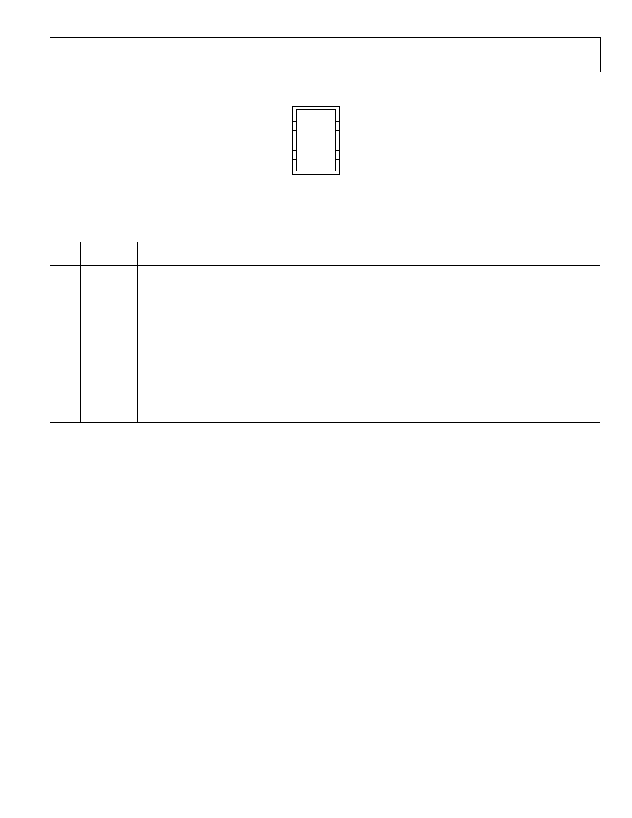
PIN CONFIGURATION AND FUNCTION DESCRIPTIONS
1
INHI
2
COMM
3
CLPF
4
VSET
8 INLO
7 VPOS
6 TADJ
5 VOUT
TOP VIEW
(Not to Scale)
AD8317
05541-002
Figure 2. Pin Configuration
Table 3. Pin Function Descriptions
Pin
No.
Mnemonic Description
1 INHI
RF Input. Nominal input range of -50 dBm to 0 dBm, re: 50
; ac-coupled RF input.
2
COMM
Device Common. Connect to a low impedance ground plane.
3 CLPF
Loop Filter Capacitor. In measurement mode, this capacitor sets the pulse response time and video bandwidth. In
controller mode, the capacitance on this node sets the response time of the error amplifier/integrator.
4
VSET
Setpoint Control Input for Controller Mode or Feedback Input for Measurement Mode.
5 VOUT
Measurement and Controller Output. In measurement mode, VOUT provides a decreasing linear-in dB representation
of the RF input signal amplitude. In controller mode, VOUT is used to control the gain of a VGA or VVA with a positive
gain sense (increasing voltage increases gain).
6 TADJ
Temperature Compensation Adjustment. Frequency-dependent temperature compensation is set by connecting a
ground-referenced resistor to this pin.
7
VPOS
Positive Supply Voltage: 3.0 V to 5.5 V.
8
INLO
RF Common for INHI. AC-coupled RF common.
Paddle
Internally connected to COMM; solder to a low impedance ground plane.
AD8317
Rev. 0 | Page 8 of 20
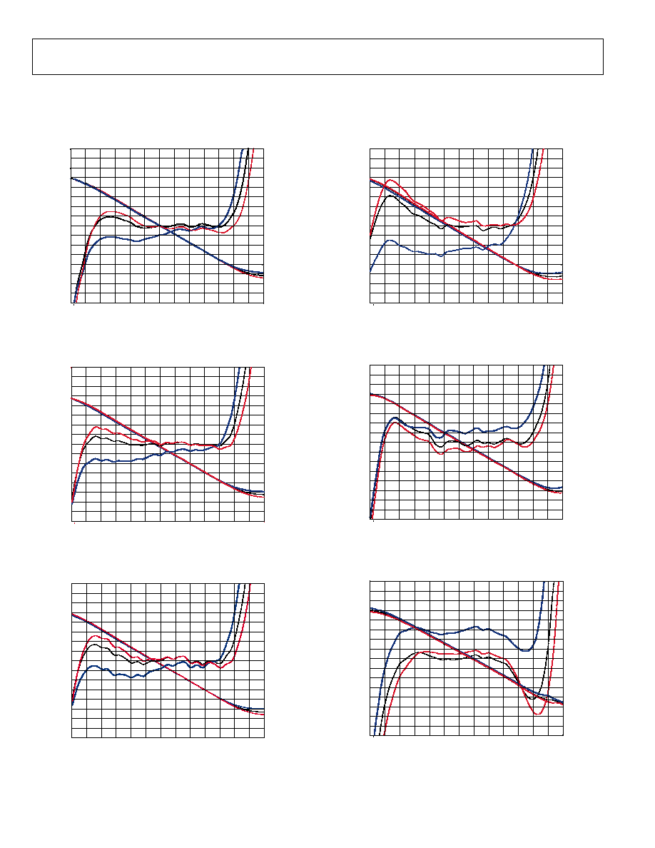
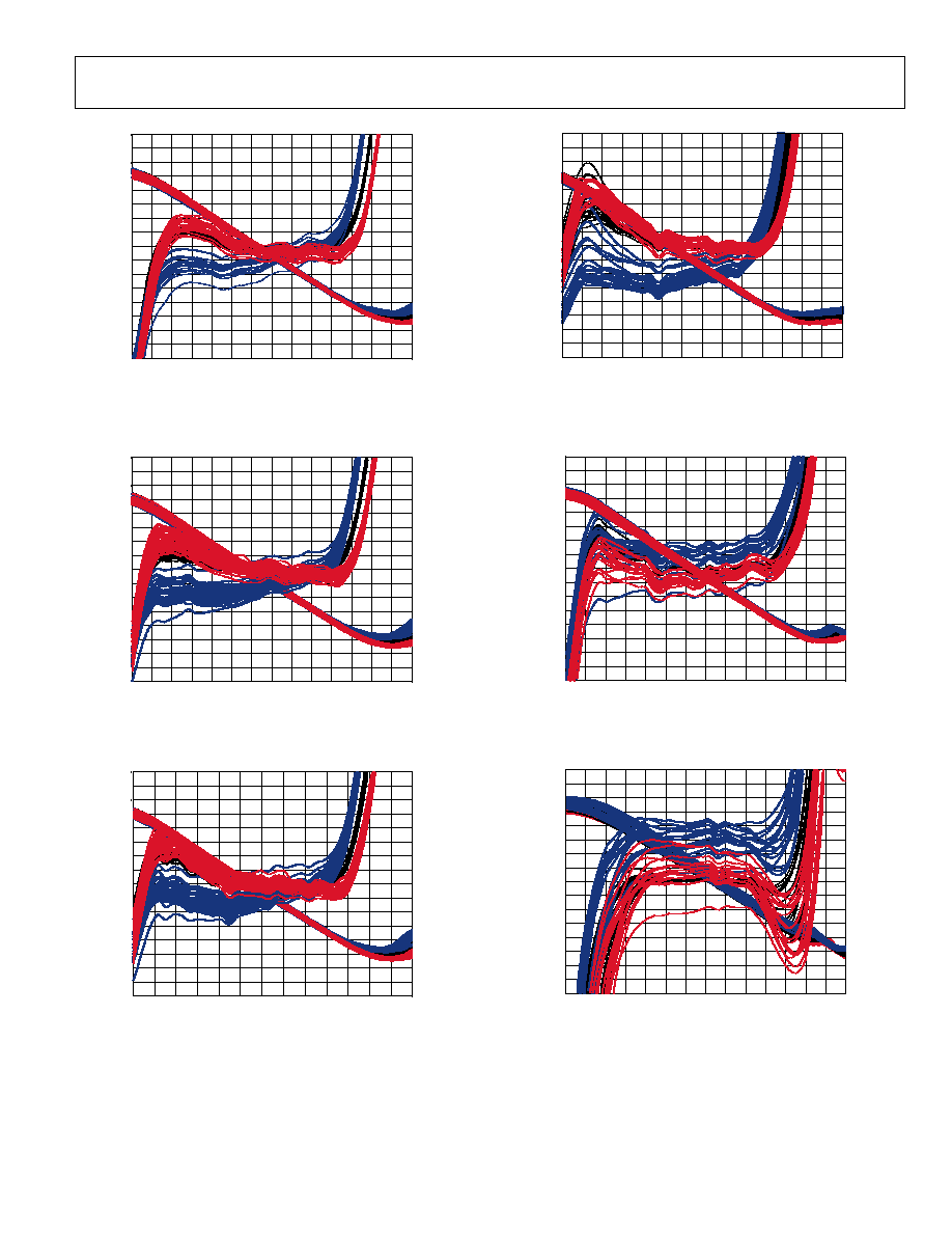
TYPICAL PERFORMANCE CHARACTERISTICS
V
POS
= 3 V; T = 25∞C, ≠40∞C, +85∞C; C
LPF
= 1000 pF, unless otherwise noted. Colors: 25∞C Black; -40∞C Blue; 85∞C Red.
Error is calculated by using the best-fit line between P
IN
= -40 dBm and P
IN
= -10 dBm at the specified input frequency, unless otherwise noted
0
0.25
0.50
1.00
1.25
1.50
1.75
2.00
V
OUT
(V
)
0.75
E
RROR (dB)
≠2.0
≠1.5
0
0.5
1.0
1.5
2.0
≠0.5
≠1.0
≠60 ≠55 ≠50 ≠45 ≠40 ≠35 ≠30 ≠25 ≠20 ≠15 ≠10 ≠5
0
5
P
IN
(dBm)
05541-003
Figure 3. V
OUT
and Log Conformance vs. Input Amplitude at 900 MHz,
R
TADJ
= 18 k
0
0.25
0.50
1.00
1.25
1.50
1.75
2.00
V
OUT
(V
)
0.75
≠2.0
≠1.5
0
0.5
1.0
1.5
2.0
E
RROR (dB)
≠0.5
≠1.0
≠60 ≠55 ≠50 ≠45 ≠40 ≠35 ≠30 ≠25 ≠20 ≠15 ≠10 ≠5
0
5
P
IN
(dBm)
05541-004
Figure 4. V
OUT
and Log Conformance vs. Input Amplitude at 1.9 GHz,
R
TADJ
= 8 k
05541-005
≠60 ≠55 ≠50 ≠45 ≠40 ≠35 ≠30 ≠25 ≠20 ≠15 ≠10 ≠5
0
5
0
0.25
0.50
0.75
1.00
1.25
1.50
1.75
P
IN
(dBm)
V
OUT
(V
)
2.00
E
RROR (dB)
≠2.0
≠1.5
0
0.5
1.0
1.5
2.0
≠0.5
≠1.0
Figure 5. V
OUT
and Log Conformance vs. Input Amplitude at 2.2 GHz,
R
TADJ
= 8 k
0
0.25
0.50
1.00
1.25
1.50
1.75
2.00
V
OUT
(V
)
0.75
≠2.0
≠1.5
0
0.5
1.0
1.5
2.0
E
RROR (dB)
≠0.5
≠1.0
≠60 ≠55 ≠50 ≠45 ≠40 ≠35 ≠30 ≠25 ≠20 ≠15 ≠10 ≠5
0
5
P
IN
(dBm)
05541-006
Figure 6. V
OUT
and Log Conformance vs. Input Amplitude at 3.6 GHz,
R
TADJ
= 8 k
0
0.25
0.50
1.00
1.25
1.50
1.75
2.00
V
OUT
(V
)
0.75
≠2.0
≠1.5
0
0.5
1.0
1.5
2.0
E
RROR (dB)
≠0.5
≠1.0
≠60 ≠55 ≠50 ≠45 ≠40 ≠35 ≠30 ≠25 ≠20 ≠15 ≠10 ≠5
0
5
P
IN
(dBm)
05541-007
Figure 7. V
OUT
and Log Conformance vs. Input Amplitude at 5.8 GHz,
R
TADJ
= 500
0
0.25
0.50
1.00
1.25
1.50
1.75
2.00
V
OUT
(V
)
0.75
≠2.0
≠1.5
0
0.5
1.0
1.5
2.0
E
RROR (dB)
≠0.5
≠1.0
≠60 ≠55 ≠50 ≠45 ≠40 ≠35 ≠30 ≠25 ≠20 ≠15 ≠10 ≠5
0
5
P
IN
(dBm)
05541-008
Figure 8. V
OUT
and Log Conformance vs. Input Amplitude at 8.0 GHz,
R
TADJ
= Open, Error Calculated from P
IN
= -34 dBm to P
IN
= -16 dBm
AD8317
Rev. 0 | Page 9 of 20
0
0.25
0.50
1.00
1.25
1.50
1.75
2.00
V
OUT
(V
)
0.75
≠2.0
≠1.5
0
0.5
1.0
1.5
2.0
E
RROR (dB)
≠0.5
≠1.0
P
IN
(dBm)
05541-009
≠60 ≠55 ≠50 ≠45 ≠40 ≠35 ≠30 ≠25 ≠20 ≠15 ≠10 ≠5
0
5
10
Figure 9. V
OUT
and Log Conformance vs. Input Amplitude at 900 MHz,
Multiple Devices, R
TADJ
= 18 k
0
0.25
0.50
1.00
1.25
1.50
1.75
2.00
V
OUT
(V
)
0.75
≠2.0
≠1.5
0
0.5
1.0
1.5
2.0
E
RROR (dB)
≠0.5
≠1.0
P
IN
(dBm)
05541-010
≠60 ≠55 ≠50 ≠45 ≠40 ≠35 ≠30 ≠25 ≠20 ≠15 ≠10 ≠5
0
5
10
Figure 10. V
OUT
and Log Conformance vs. Input Amplitude at 1.9 GHz,
Multiple Devices, R
TADJ
= 8 k
0
0.25
0.50
1.00
1.25
1.50
1.75
2.00
V
OUT
(V
)
0.75
≠2.0
≠1.5
0
0.5
1.0
1.5
2.0
E
RROR (dB)
≠0.5
≠1.0
05541-011
P
IN
(dBm)
≠60 ≠55 ≠50 ≠45 ≠40 ≠35 ≠30 ≠25 ≠20 ≠15 ≠10 ≠5
0
5
Figure 11. V
OUT
and Log Conformance vs. Input Amplitude at 2.2 GHz,
Multiple Devices, R
TADJ
= 8 k
≠1.5
≠1.0
≠0.5
0
0.5
1.0
1.5
2.00
0
05541-012
P
IN
(dBm)
V
OUT
(V
)
0.25
0.50
0.75
1.00
1.25
1.50
1.75
2.0
≠2.0
E
RROR (dB)
≠60 ≠55 ≠50 ≠45 ≠40 ≠35 ≠30 ≠25 ≠20 ≠15 ≠10 ≠5
0
5
10
Figure 12. V
OUT
and Log Conformance vs. Input Amplitude at 3.6 GHz,
Multiple Devices, R
TADJ
= 8 k
0
0.25
0.50
1.00
1.25
1.50
1.75
2.00
V
OUT
(V
)
0.75
≠2.0
≠1.5
0
0.5
1.0
1.5
2.0
E
RROR (dB)
≠0.5
≠1.0
P
IN
(dBm)
05541-013
≠60 ≠55 ≠50 ≠45 ≠40 ≠35 ≠30 ≠25 ≠20 ≠15 ≠10 ≠5
0
5
10
Figure 13. V
OUT
and Log Conformance vs. Input Amplitude at 5.8 GHz,
Multiple Devices, R
TADJ
= 500
0
0.25
0.50
1.00
1.25
1.50
1.75
2.00
V
OUT
(V
)
0.75
≠2.0
≠1.5
0
0.5
1.0
1.5
2.0
E
RROR (dB)
≠0.5
≠1.0
P
IN
(dBm)
05541-014
≠60 ≠55 ≠50 ≠45 ≠40 ≠35 ≠30 ≠25 ≠20 ≠15 ≠10 ≠5
0
5
10
Figure 14. V
OUT
and Log Conformance vs. Input Amplitude at 8.0 GHz,
Multiple Devices, R
TADJ
=Open,
Error Calculated from P
IN
= -34 dBm to P
IN
= -16 dBm
AD8317
Rev. 0 | Page 10 of 20
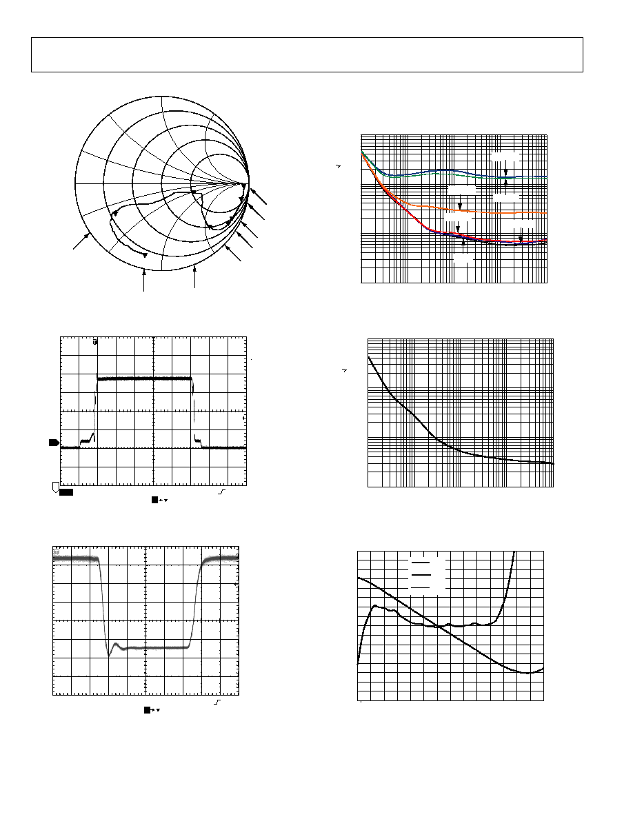
0
j2
j1
≠j1
≠j2
j0.5
≠j0.5
j0.2
≠j0.2
0.2
0.5
1
2
8000MHz
10000MHz
5800MHz
3600MHz
2200MHz
1900MHz
900MHz
100MHz
START FREQUENCY = 0.05GHz
STOP FREQUENCY = 10GHz
05541-
015
Figure 15. Input Impedance vs. Frequency; No Termination Resistor on INHI
(Impedance De-Embedded to Input Pins), Z
0
= 50
A Ch3 620mV
3
05541-017
Ch3
500mV Ch4 200mV
M4.00
s
T
12.7560
s
4
: 1.86V
@ : 1.69V
Figure 16. Power On/Off Response Time; V
P
= 3.0 V;
Input AC-Coupling Caps = 10 pF; C
LPF
= Open
CH1 200mV
05541-016
M20.0ns
A CH1 1.40V
T
943.600ns
Ch1 RISE
10.44ns
Ch1 FALL
6.113ns
Figure 17. V
OUT
Pulse Response Time; Pulsed RF Input 0.1 GHz, -10 dBm;
C
LPF
= Open; R
LOAD
= 150
05541-018
1k
10k
100k
1M
10
100
1000
10000
10M
N
OISE SPEC
TR
A
L
D
E
N
S
ITY (
n
V/ H
z
)
≠20dBm
0dBm
≠60dBm
RF OFF
≠40dBm
FREQUENCY (Hz)
≠10dBm
Figure 18. Noise Spectral Density of Output; C
LPF
= Open
05541-019
1k
10k
100k
1M
10
100
1000
10000
10M
N
OISE SPEC
TR
A
L
D
E
N
S
ITY (
n
V/ H
z
)
FREQUENCY (Hz)
Figure 19. Noise Spectral Density of Output Buffer (from CLPF to VOUT);
C
LPF
= 0.1 F
0
0.25
0.50
1.00
1.25
1.50
1.75
2.00
V
OUT
(V
)
0.75
E
RROR (dB)
≠2.0
≠1.5
0
0.5
1.0
1.5
2.0
≠0.5
≠1.0
≠55 ≠50 ≠45 ≠40 ≠35 ≠30 ≠25 ≠20 ≠15 ≠10 ≠5
0
5
10
P
IN
(dBm)
≠60
3.3V
3.0V
3.6V
05541-020
Figure 20. Output Voltage Stability vs. Supply Voltage at 1.9 GHz
When V
POS
Varies by 10%
AD8317
Rev. 0 | Page 11 of 20
THEORY OF OPERATION
The AD8317 is a 6-stage demodulating logarithmic amplifier,
specifically designed for use in RF measurement and power control
applications at frequencies up to 10 GHz. A block diagram is
shown in Figure 21. Sharing much of its design with the AD8318
logarithmic detector/controller, the AD8317 maintains tight inter-
cept variability vs. temperature over a 50 dB range. Additional
enhancements over the AD8318, such as reduced RF burst
response time of 8 ns to 10 ns, 22 mA supply current, and board
space requirements of only 2 mm x 3 mm, add to the low cost
and high performance benefits found in the AD8317.
GAIN
BIAS
SLOPE
DET
DET
DET
DET
INHI
INLO
I
V
VOUT
VSET
CLPF
TADJ
VPOS
COMM
05541-021
I
V
Figure 21. Block Diagram
A fully differential design, using a proprietary, high speed SiGe
process, extends high frequency performance. Input INHI receives
the signal with a low frequency impedance of nominally 500
in parallel with 0.7 pF. The maximum input with ±1 dB log-
conformance error is typically 0 dBm (re: 50 ). The noise
spectral density referred to the input is 1.15 nV/Hz, which is
equivalent to a voltage of 118 V rms in a 10.5 GHz bandwidth
or a noise power of -66 dBm (re: 50 ). This noise spectral
density sets the lower limit of the dynamic range. However, the
low end accuracy of the AD8317 is enhanced by specially shaping
the demodulating transfer characteristic to partially compensate
for errors due to internal noise. The common pin, COMM,
provides a quality low impedance connection to the printed circuit
board (PCB) ground. The package paddle, which is internally
connected to the COMM pin, should also be grounded to the
PCB to reduce thermal impedance from the die to the PCB.
The logarithmic function is approximated in a piecewise
fashion by six cascaded gain stages. (For a more comprehensive
explanation of the logarithm approximation, please refer to the
AD8307 data sheet, available at www.analog.com.) The cells
have a nominal voltage gain of 9 dB each and a 3 dB bandwidth
of 10.5 GHz. Using precision biasing, the gain is stabilized over
temperature and supply variations. The overall dc gain is high,
due to the cascaded nature of the gain stages. An offset
compensation loop is included to correct for offsets within the
cascaded cells. At the output of each of the gain stages, a square-
law detector cell is used to rectify the signal.
The RF signal voltages are converted to a fluctuating differential
current having an average value that increases with signal level.
Along with the six gain stages and detector cells, an additional
detector is included at the input of the AD8317, providing a 50 dB
dynamic range in total. After the detector currents are summed
and filtered, the following function is formed at the summing node:
I
D
◊ log
10
(V
IN
/V
INTERCEPT
)
where:
I
D
is the internally set detector current.
V
IN
is the input signal voltage.
V
INTERCEPT
is the intercept voltage (that is, when V
IN
= V
INTERCEPT
,
the output voltage would be 0 V, if it were capable of going to 0 V).
AD8317
Rev. 0 | Page 12 of 20
USING THE AD8317
BASIC CONNECTIONS
The AD8317 is specified for operation up to 10 GHz; as a result,
low impedance supply pins with adequate isolation between
functions are essential. A power supply voltage of between 3.0 V
and 5.5 V should be applied to VPOS. Power supply decoupling
capacitors of 100 pF and 0.1 F should be connected close to
this power supply pin.
AD8317
1
2
3
4
8
7
6
5
SIGNAL
INPUT
R1
52.3
R2
0
R4
0
V
OUT
C2
C1
C5
C4
47nF
47nF
SEE TEXT
SEE TEXT
0.1
F
100pF
V
S
(2.7V≠5.5V)
INHI
INLO
VPOS
TADJ
VOUT
COMM
CLPF
VSET
05
54
1-
0
22
Figure 22. Basic Connections
The paddle of the LFCSP_VD package is internally connected
to COMM. For optimum thermal and electrical performance,
the paddle should be soldered to a low impedance ground plane.
INPUT SIGNAL COUPLING
The RF input (INHI) is single-ended and must be ac-coupled.
INLO (input common) should be ac-coupled to ground.
Suggested coupling capacitors are 47 nF ceramic 0402-style
capacitors for input frequencies of 1 MHz to 10 GHz. The
coupling capacitors should be mounted close to the INHI and
INLO pins. The coupling capacitor values can be increased to
lower the input stage's high-pass cutoff frequency. The high-pass
corner is set by the input coupling capacitors and the internal
10 pF high-pass capacitor. The dc voltage on INHI and INLO is
about one diode voltage drop below V
POS
.
05541-023
VPOS
2k
A = 9dB
18.7k
18.7k
CURRENT
Gm
STAGE
INLO
INHI
OFFSET
COMP
5pF
5pF
FIRST
GAIN
STAGE
Figure 23. Input Interface
While the input can be reactively matched, in general this is not
necessary. An external 52.3 shunt resistor (connected on the
signal side of the input coupling capacitors, as shown in
Figure 22) combines with the relatively high input impedance
to give an adequate broadband 50 match.
The coupling time constant, 50 ◊ C
C
/2, forms a high-pass
corner with a 3 dB attenuation at f
HP
= 1/(2 ◊ 50 ◊ C
C
), where
C1 = C2 = C
C
. Using the typical value of 47 nF, this high pass
corner will be ~68 kHz. In high frequency applications, f
HP
should be as large as possible to minimize the coupling of
unwanted low frequency signals. In low frequency applications,
a simple RC network forming a low-pass filter should be added
at the input for similar reasons. This should generally be placed
at the generator side of the coupling capacitors, thereby
lowering the required capacitance value for a given high-pass
corner frequency.
OUTPUT INTERFACE
The VOUT pin is driven by a PNP output stage. An internal 10
resistor is placed in series with the output and the VOUT pin.
The rise time of the output is limited mainly by the slew on
CLPF. The fall time is an RC-limited slew given by the load
capacitance and the pull-down resistance at VOUT. There is an
internal pull-down resistor of 1.6 k. A resistive load at VOUT
is placed in parallel with the internal pull-down resistor to
provide additional discharge current.
05541-024
+
0.8V
1200
400
≠
10
VOUT
VPOS
CLPF
COMM
Figure 24. Output Interface
To reduce the fall time, VOUT should be loaded with a resistive
load of <1.6 k. For example, with an external load of 150 the
AD8317 fall time is <7 ns.
SETPOINT INTERFACE
The V
SET
input drives the high impedance (20 k) input of an
internal op amp. The V
SET
voltage appears across the internal
1.5 k resistor to generate I
SET
. When a portion of V
OUT
is applied
to VSET, the feedback loop forces
-I
D
◊ log
10
(V
IN
/V
INTERCEPT
) = I
SET
.
If V
SET
= V
OUT
/2x, then I
SET
= V
OUT
/(2x ◊ 1.5 k).
The result is
V
OUT
= (-I
D
◊ 1.5 k ◊ 2x) ◊ log
10
(V
IN
/V
INTERCEPT
)
AD8317
Rev. 0 | Page 13 of 20
05541-025
1.5k
I
SET
COMM
VSET
V
SET
COMM
20k
20k
Figure 25. VSET Interface
The slope is given by ≠I
D
◊ 2x ◊ 1.5 k = -22 mV/dB ◊ x. For
example, if a resistor divider to ground is used to generate a V
SET
voltage of V
OUT
/2, then x = 2. The slope is set to -880 V/decade
or -44 mV/dB.
TEMPERATURE COMPENSATION OF OUTPUT
VOLTAGE
The primary component of the variation in V
OUT
vs. temperature,
as the input signal amplitude is held constant, is the drift of the
intercept. This drift is also a weak function of the input signal
frequency, so provision is made for optimization of internal
temperature compensation at a given frequency by providing
Pin TADJ.
COMM
COMM
I
COMP
V
INTERNAL
TADJ
R
TADJ
05541-026
1.5k
AD8317
Figure 26. TADJ Interface
The Resistor R
TADJ
is connected between this pin and ground.
The value of this resistor partially determines the magnitude
of an analog correction coefficient, which is used to reduce
intercept drift.
The relationship between output temperature drift and
frequency is not linear and cannot be easily modeled. As
a result, experimentation is required to choose the correct
TADJ resistor. Table 4 shows the recommended values for
some commonly used frequencies.
Table 4: Recommended R
TADJ
Resistor Values
Frequency Recommended
R
TADJ
50 MHz
18 k
100 MHz
18 k
900 MHz
18 k
1.8 GHz
8 k
1.9 GHz
8 k
2.2 GHz
8 k
3.6 GHz
8 k
5.3 GHZ
500
5.8 GHz
500
8 GHz
Open
MEASUREMENT MODE
When the V
OUT
voltage or a portion of the V
OUT
voltage is fed
back to the VSET pin, the device operates in measurement
mode. As seen in Figure 27, the AD8317 has an offset voltage,
a negative slope, and a V
OUT
measurement intercept at the high
end of its input signal range.
0
0.25
0.50
0.75
1.00
1.25
1.50
2.00
V
OUT
(V
)
≠1.5
≠1.0
≠0.5
0
0.5
1.0
1.5
2.0
≠60 ≠55 ≠50 ≠45 ≠40 ≠35 ≠30 ≠25 ≠20 ≠15 ≠10 ≠5
0
5
10 15
P
IN
(dBm)
05541-027
RANGE FOR
CALCULATION OF
SLOPE AND INTERCEPT
V
OUT
25∞C
ERROR 25∞C
1.75
INTERCEPT
Figure 27. Typical Output Voltage vs. Input Signal
The output voltage vs. input signal voltage of the AD8317 is
linear-in-dB over a multidecade range. The equation for this
function is of the form
V
OUT
= X ◊ V
SLOPE/DEC
◊ log
10
(V
IN
/V
INTERCEPT
) =
(1)
X ◊ V
SLOPE/dB
◊ 20 ◊ log
10
(V
IN
/V
INTERCEPT
) (2)
where:
X is the feedback factor in V
SET
= V
OUT
/X.
V
SLOPE/DEC
is nominally ≠440 mV/decade or -22 mV/dB.
V
INTERCEPT
is the x-axis intercept of the linear-in-dB portion of
the V
OUT
vs. V
IN
curve (Figure 27).
V
INTERCEPT
is +2 dBV for a sinusoidal input signal.
An offset voltage, V
OFFSET
, of 0.35 V is internally added to the
detector signal, so that the minimum value for V
OUT
is
X ◊ V
OFFSET
. So for X = 1, minimum V
OUT
is 0.35 V.
The slope is very stable vs. process and temperature variation.
When base-10 logarithms are used, V
SLOPE/DECADE
represents the
volts/decade. A decade corresponds to 20 dB; V
SLOPE/DECADE
/20 =
V
SLOPE/dB
represents the slope in volts/dB.
As noted in Equation 1 and Equation 2, the V
OUT
voltage has a
negative slope. This is also the correct slope polarity to control
the gain of many power amplifiers in a negative feedback
configuration. Because both the slope and intercept vary slightly
with frequency, it is recommended to refer to the Specifications
section for application-specific values for slope and intercept.
AD8317
Rev. 0 | Page 14 of 20
Although demodulating log amps respond to input signal voltage,
not input signal power, it is customary to discuss the amplitude
of high frequency signals in terms of power. In this case, the charac-
teristic impedance of the system, Z
0
, must be known to convert
voltages to their corresponding power levels. The following
equations are used to perform this conversion:
P(dBm) = 10 ◊ log
10
(V
rms
2
/(Z
0
◊ 1 mW))
(3)
P(dBV) = 20 ◊ log
10
(V
rms
/1 V
rms
) (4)
P(dBm) = P(dBV) - 10 ◊ log
10
(Z
0
◊ 1 mW/1 V
rms
2
) (5)
For example, P
INTERCEPT
for a sinusoidal input signal expressed in
terms of dBm (decibels referred to 1 mW), in a 50 system is
P
INTERCEPT
(dBm) = P
INTERCEPT
(dBV) ≠ 10 ◊ log
10
(Z
0
◊
1 mW/1 V
rms
2
) =
(6)
+2 dBV - 10 ◊ log
10
(50◊10
-3
) = +15 dBm
For a square wave input signal in a 200 system,
P
INTERCEPT
= -1 dBV - 10 ◊ log
10
[(200 ◊ 1 mW/1V
rms
2
)] =
+6 dBm
Further information on the intercept variation dependence upon
waveform can be found in the AD8313 and AD8307 data sheets.
SETTING THE OUTPUT SLOPE
IN MEASUREMENT MODE
To operate in measurement mode, VOUT must be connected to
VSET. Connecting VOUT directly to VSET yields the nominal
logarithmic slope of approximately -22 mV/dB. The output
swing corresponding to the specified input range is then approxi-
mately 0.35 V to 1.7 V. The slope and output swing can be
increased by placing a resistor divider between VOUT and
VSET (that is, one resistor from VOUT to VSET and one
resistor from VSET to ground). The input impedance of VSET
is approximately 40 k. Slope-setting resistors should be kept
below 20 k to prevent this input impedance from affecting
the resulting slope. If two equal resistors are used (for example,
10 k/10 k), the slope doubles to approximately -44 mV/dB.
05541-028
VOUT
AD8317
≠44mV/dB
VSET
10k
10k
Figure 28. Increasing the Slope
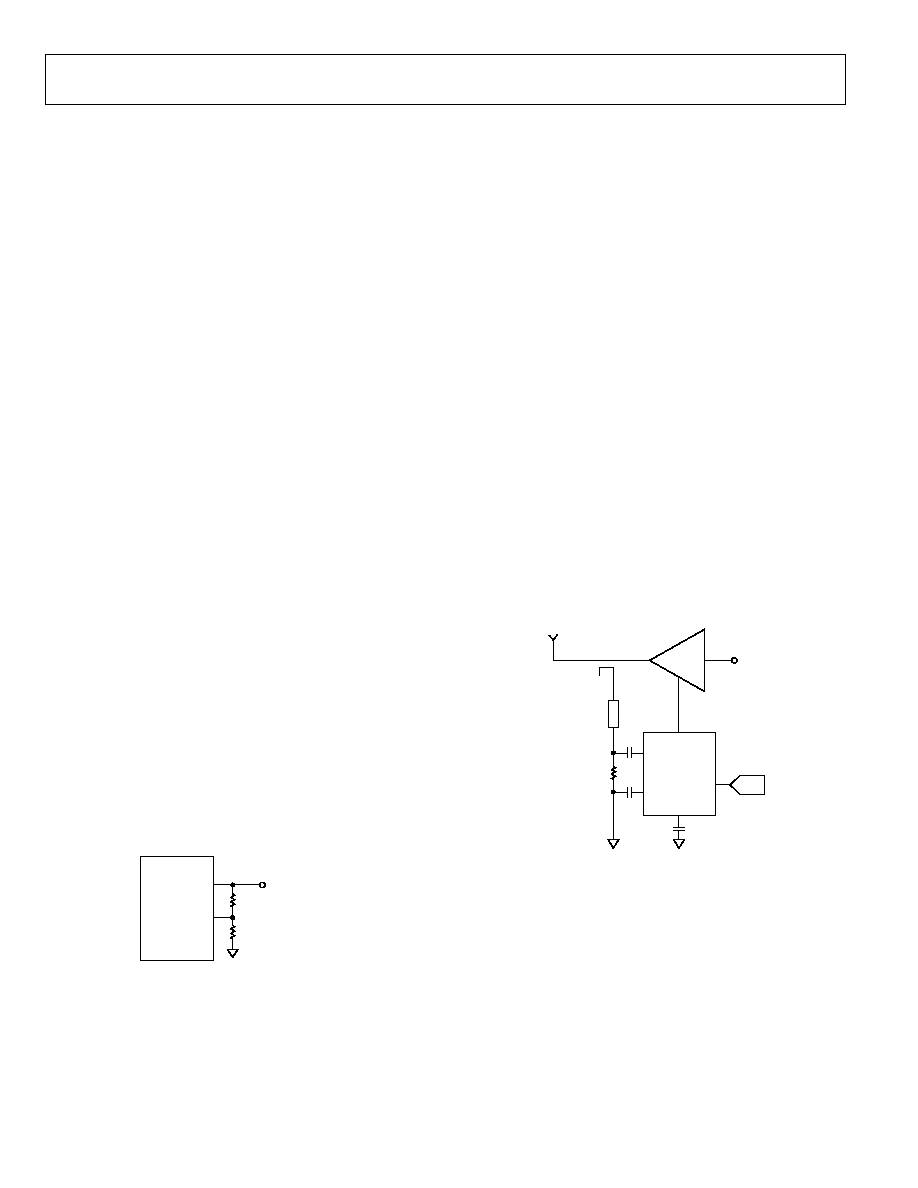
CONTROLLER MODE
The AD8317 provides a controller mode feature at the VOUT
pin. Using V
SET
for the setpoint voltage, it is possible for the
AD8317 to control subsystems, such as power amplifiers (PAs),
variable gain amplifiers (VGAs), or variable voltage attenuators
(VVAs) that have output power that increases monotonically
with respect to their gain control signal.
To operate in controller mode, the link between VSET and
VOUT is broken. A setpoint voltage is applied to the VSET
input, VOUT is connected to the gain control terminal of the
variable gain amplifier (VGA), and the detector's RF input is
connected to the output of the VGA (usually using a directional
coupler and some additional attenuation). Based on the defined
relationship between V
OUT
and the RF input signal when the device
is in measurement mode, the AD8317 adjusts the voltage on
VOUT (VOUT is now an error amplifier output) until the level
at the RF input corresponds to the applied V
SET
. When the AD8317
operates in controller mode, there is no defined relationship
between V
SET
and V
OUT
voltage; V
OUT
settles to a value that results in
the correct input signal level appearing at INHI/INLO.
For this output power control loop to be stable, a ground-
referenced capacitor must be connected to the CLPF pin. This
capacitor, C
FLT
, integrates the error signal (in the form of a
current) to set the loop bandwidth and ensure loop stability.
Further details on control loop dynamics can be found in the
AD8315 data sheet.
05541-029
RFIN
VGA/VVA
GAIN
CONTROL
VOLTAGE
DIRECTIONAL
COUPLER
ATTENUATOR
INHI
VSET
INLO
CLPF
VOUT
AD8317
52.3
47nF
C
FLT
47nF
DAC
Figure 29. AD8317 Controller Mode
Decreasing V
SET
, which corresponds to demanding a higher
signal from the VGA, increases V
OUT
. The gain control voltage
of the VGA must have a positive sense. A positive control
voltage to the VGA increases the gain of the device.
The basic connections for operating the AD8317 in an automatic
gain control (AGC) loop with the ADL5330 are shown in
Figure 30. The ADL5330 is a 10 MHz to 3 GHz variable gain
amplifier. It offers a large gain control range of 60 dB with
±0.5 dB gain stability. This configuration is similar to Figure 29.
AD8317
Rev. 0 | Page 15 of 20
The gain of the ADL5330 is controlled by the output pin of the
AD8317. This voltage, V
OUT
, has a range of 0 V to near V
POS
. To
avoid overdrive recovery issues, the AD8317 output voltage can
be scaled down using a resistive divider to interface with the 0 V
to 1.4 V gain control range of the ADL5330.
A coupler/attenuation of 21 dB is used to match the desired
maximum output power from the VGA to the top end of the
linear operating range of the AD8317 (approximately -5 dBm
at 900 MHz).
INLO
INHI
GAIN
OPLO
OPHI
DIRECTIONAL
COUPLER
ATTENUATOR
VPOS
COMM
ADL5330
+5V
+5V
+5V
COMM
VOUT
VPOS
VSET
INHI
INLO
CLPF
AD8317
LOG AMP
DAC
RF OUTPUT
SIGNAL
4.12k
10k
SETPOINT
VOLTAGE
1nF
47nF
47nF
120nH
120nH
100pF
100pF
100pF
100pF
TADJ
18k
52.3
RF INPUT
SIGNAL
05541-
030
Figure 30. AD8317 Operating in Controller Mode to Provide Automatic
Gain Control Functionality in Combination with the ADL5330
Figure 31 shows the transfer function of the output power vs.
the V
SET
voltage over temperature for a 900 MHz sine wave with
an input power of -1.5 dBm. Note that the power control of the
AD8317 has a negative sense. Decreasing V
SET
, which corresponds
to demanding a higher signal from the ADL5330, increases gain.
The AGC loop is capable of controlling signals just under the
full 60 dB gain control range of the ADL5330. The performance
over temperature is most accurate over the highest power range,
where it is generally most critical. Across the top 40 dB range of
output power, the linear conformance error is well within ±0.5 dB
over temperature.
≠50
≠40
≠30
≠10
0
10
20
30
OUTP
UT P
O
WE
R (dBm)
≠20
≠4
≠3
0
1
2
3
4
≠1
≠2
0.2
0.4
0.6
0.8
1
1.4
1.8
2.0
SETPOINT VOLTAGE (V)
1.6
1.2
05541-031
Figure 31. ADL5330 Output Power vs. AD8317 Setpoint Voltage,
P
IN
= -1.5 dBm
For the AGC loop to remain in equilibrium, the AD8317 must
track the envelope of the ADL5330's output signal and provide
the necessary voltage levels to the ADL5330 gain control input.
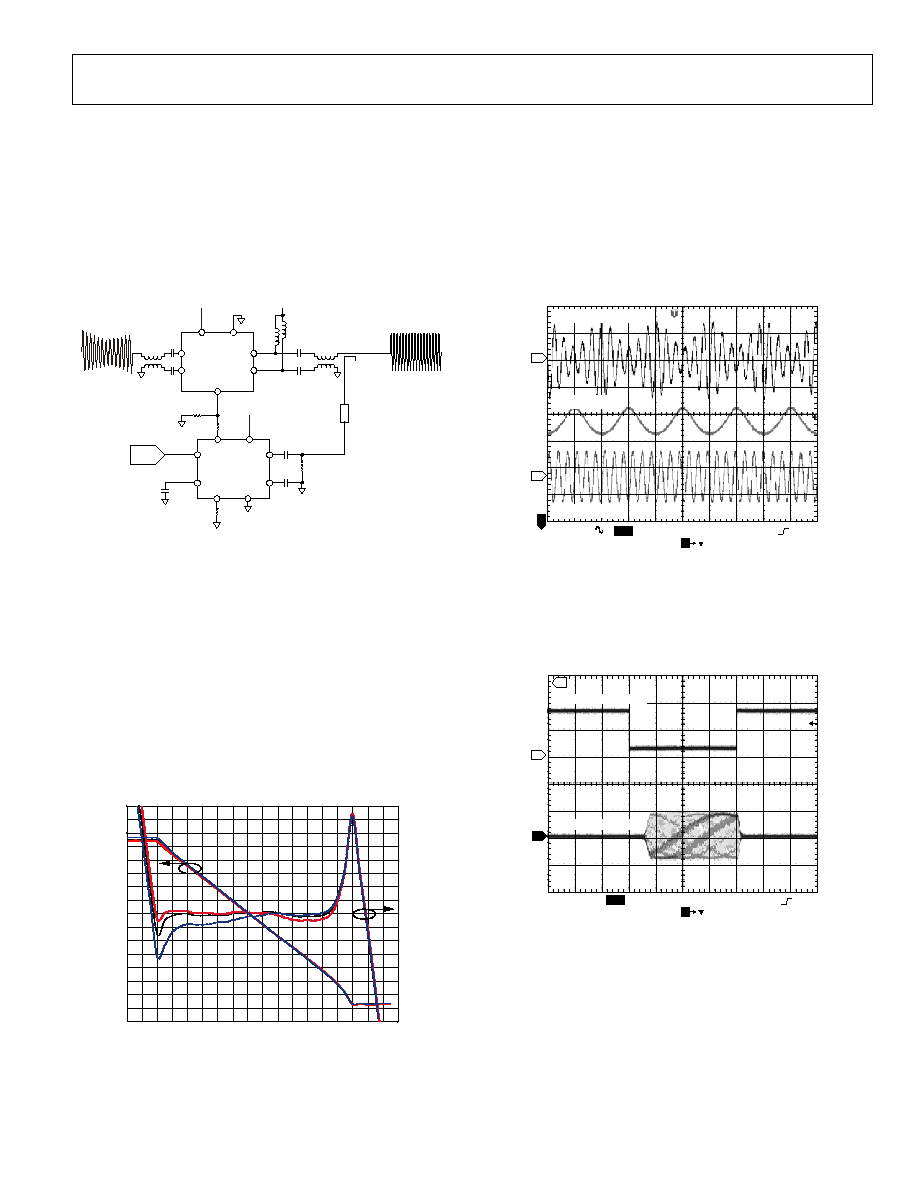
Figure 32 shows an oscilloscope screenshot of the AGC loop
depicted in Figure 30. A 100 MHz sine wave with 50% AM
modulation is applied to the ADL5330. The output signal from
the VGA is a constant envelope sine wave with amplitude corre-
sponding to a setpoint voltage at the AD8317 of 1.5 V. Also shown
is the gain control response of the AD8317 to the changing input
envelope.
CH1 200mV
CH3 50.0mV
A Ch2 820mV
05541-032
M2.00ms
T
640.00
s
1
3
2
AM MODULATED INPUT
AD8317 OUTPUT
ADL5330 OUTPUT
Ch2
200mV
Figure 32. Oscilloscope Screenshot Showing an AM Modulated Input Signal
and the Response from the AD8317
Figure 33 shows the response of the AGC RF output to a pulse
on VSET. As V
SET
decreases from 1.7 V to 0.4 V, the AGC loop
responds with an RF burst. In this configuration the input signal to
the ADL5330 is a 1 GHz sine wave at a power level of -15 dBm.
05541-033
A CH1 2.48V
T
699.800
s
AD8317 VSET PULSE
ADL5330 OUTPUT
2
1
T
M10.0
s
CH1 2.00V
CH2
50mV
Figure 33. Oscilloscope Screenshot Showing
the Response Time of the AGC Loop
Response time and the amount of signal integration are
controlled by C
FLT
. This functionality is analogous to the
feedback capacitor around an integrating amplifier. While
it is possible to use large capacitors for C
FLT
, in most applica-
tions values under 1 nF provide sufficient filtering.
AD8317
Rev. 0 | Page 16 of 20
Calibration in controller mode is similar to the method used in
measurement mode. A simple two-point calibration can be
done by applying two known V
SET
voltages or DAC codes and
measuring the output power from the VGA. Slope and intercept
can then be calculated with the following equations:
Slope = (V
SET1
- V
SET2
)/(P
OUT1
- P
OUT2
) (7)
Intercept = P
OUT1
- V
SET1
/Slope (8)
V
SETX
= Slope ◊ (P
OUTX
- Intercept) (9)
More information on the use of the ADL5330 in AGC
applications can be found in the ADL5330 data sheet.
OUTPUT FILTERING
For applications in which maximum video bandwidth and,
consequently, fast rise time are desired, it is essential that the
CLPF pin be left unconnected and free of any stray capacitance.
The nominal output video bandwidth of 50 MHz can be
reduced by connecting a ground-referenced capacitor (C
FLT
) to
the CLPF pin, as shown in Figure 34. This is generally done to
reduce output ripple (at twice the input frequency for a
symmetric input waveform such as sinusoidal signals).
+4
VOUT
CLPF
AD8317
3.5pF
05541-037
I
LOG
C
FLT
1.5k
Figure 34. Lowering the Postdemodulation Bandwidth
C
FLT
is selected using the following equation:
(
)
pF
5
.
3
k
5
.
1
1
-
◊
◊
=
Bandwidth
Video
C
FLT
(10)
The video bandwidth should typically be set to a frequency
equal to about one-tenth the minimum input frequency. This
ensures that the output ripple of the demodulated log output,
which is at twice the input frequency, is well filtered.
In many log amp applications, it may be necessary to lower the
corner frequency of the postdemodulation filtering to achieve
low output ripple while maintaining a rapid response time to
changes in signal level. An example of a 4-pole active filter is
shown in the AD8307 data sheet.
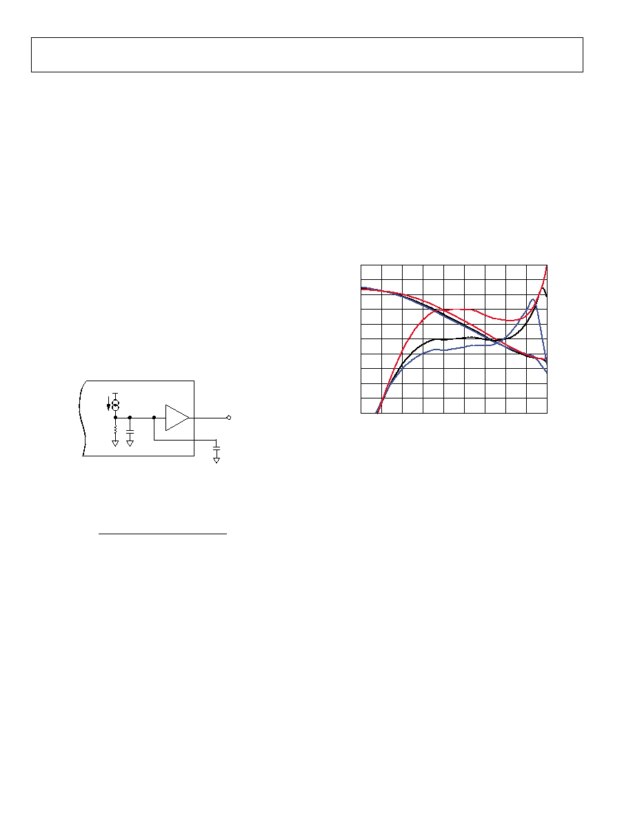
OPERATION BEYOND 8 GHZ
The AD8317 is specified for operation up to 8 GHz, but it
provides useful measurement accuracy over a reduced dynamic
range of up to 10 GHz. Figure 35 shows the performance of the
AD8317 over temperature at 10 GHz when the device is config-
ured as shown in Figure 22. Dynamic range is reduced at this
frequency, but the AD8317 does provide 30 dB of measurement
range within ±3 dB of linearity error.
05541-038
0
0.2
0.4
0.6
0.8
1.0
1.2
1.4
1.6
1.8
2.0
≠40
≠35
≠30
≠25
≠20
≠15
≠10
≠5
0
5
P
IN
(dBm)
V
OUT
(V
)
≠5
≠4
≠3
≠2
≠1
0
1
2
3
4
5
E
RROR (dB)
Figure 35. V
OUT
and Log Conformance vs. Input Amplitude at 10.0 GHz, Multiple
Devices, R
TADJ
= Open, C
LPF
= 1000 pF
Implementing an impedance match for frequencies beyond 8 GHz
can improve the sensitivity of the AD8317 and measurement
range.
Operation beyond 10 GHz is possible, but part-to-part
variation, most notably in the intercept, becomes significant.

AD8317
Rev. 0 | Page 17 of 20
EVALUATION BOARD
Table 5. Evaluation Board (Rev. A) Configuration Options
Component Function
Default
Conditions
VPOS, GND
Supply and Ground Connections. Not
applicable
R1, C1, C2
Input Interface.
The 52.3
resistor in position R1 combines with the AD8317's internal input
impedance to give a broadband input impedance of about 50
. Capacitor
C1 and Capacitor C2 are dc-blocking capacitors. A reactive impedance
match can be implemented by replacing R1 with an inductor and C1 and C2
with appropriately valued capacitors.
R1 = 52.3
(Size 0402)
C1 = 47 nF (Size 0402)
C2 = 47 nF (Size 0402)
R5, R7
Temperature Compensation Interface.
The internal temperature compensation network is optimized for input signals
up to 3.6 GHz when R7 is 10 k
. This circuit can be adjusted to optimize
performance for other input frequencies by changing the value of the
resistor in position R7. See Table 4 for specific T
ADJ
resistor values.
R5 = 200
(Size 0402)
R7 = open (Size 0402)
R2, R3, R4, R6, RL,
CL
Output Interface--Measurement Mode.
In measurement mode, a portion of the output voltage is fed back to Pin VSET
via R2. The magnitude of the slope of the VOUT output voltage response can
be increased by reducing the portion of V
OUT
that is fed back to VSET. R6 can
be used as a back-terminating resistor or as part of a single-pole, low-pass
filter.
R2 = 0
(Size 0402)
R3 = open (Size 0402)
R4 = open (Size 0402)
R6 = 1 k
(Size 0402)
RL = CL = open (Size 0402)
R2, R3
Output Interface--Controller Mode.
In this mode, R2 must be open. In controller mode, the AD8317 can control the
gain of an external component. A setpoint voltage is applied to Pin VSET, the
value of which corresponds to the desired RF input signal level applied to the
AD8317 RF input. A sample of the RF output signal from this variable-gain
component is selected, typically via a directional coupler, and applied to
AD8317 RF input. The voltage at Pin VOUT is applied to the gain control of
the variable gain element. A control voltage is applied to Pin VSET. The
magnitude of the control voltage can optionally be attenuated via the
voltage divider comprising R2 and R3, or a capacitor can be installed in
position R3 to form a low-pass filter along with R2.
R2 = open (Size 0402)
R3 = open (Size 0402)
C4, C5,
Power Supply Decoupling.
The nominal supply decoupling consists of a 100 pF filter capacitor placed
physically close to the AD8317 and a 0.1 F capacitor placed nearer to the
power supply input pin.
C5 = 100 pF (Size 0402)
C4 = 0.1 F (Size 0603)
C3 Filter
Capacitor.
The low-pass corner frequency of the circuit that drives Pin VOUT can be
lowered by placing a capacitor between CLPF and ground. Increasing this
capacitor increases the overall rise/fall time of the AD8317 for pulsed input
signals. See the Output Filtering section for more details.
C3 = 8.2 pF (Size 0402)
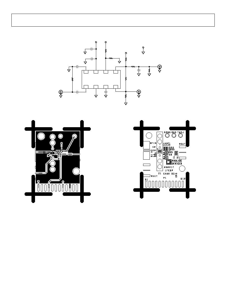
AD8317
Rev. 0 | Page 18 of 20
AD8317
1
2
3
4
8
7
6
5
R1
52.3
R7
OPEN
R2
0
C1
C2
C4
C5
47nF
47nF
0.1
F
100pF
VPOS
INHI
INLO
VPOS
TADJ
VOUT
COMM
CLPF
VSET
05541-034
TADJ
R5
200
R4
OPEN
VOUT_ALT
R3
OPEN
CL
OPEN
RL
OPEN
R6
1k
GND
RFIN
V
SET
V
OUT
C3
8.2pF
Figure 36. Evaluation Board Schematic
05541-035
Figure 37. Component Side Layout
05541-036
Figure 38. Component Side Silkscreen
AD8317
Rev. 0 | Page 19 of 20
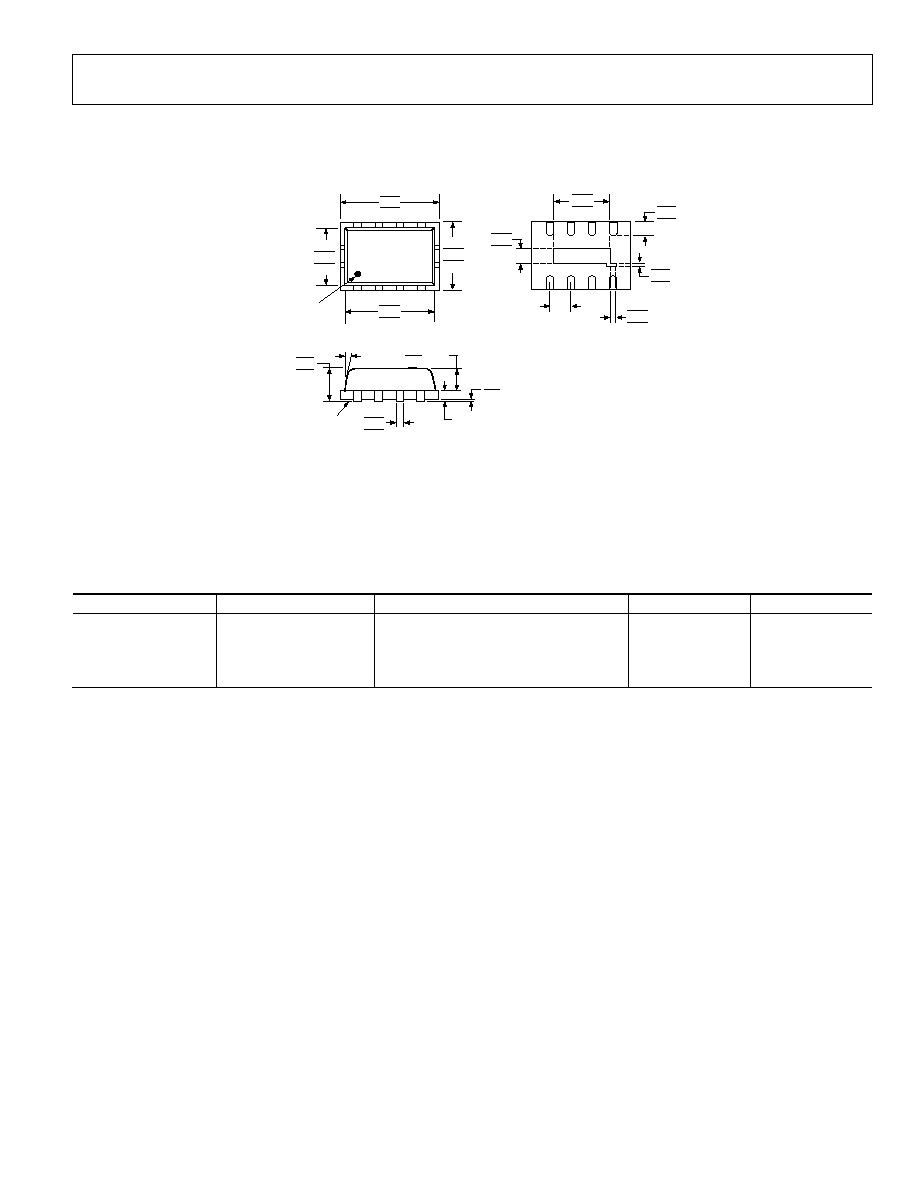
OUTLINE DIMENSIONS
0.30
0.23
0.18
SEATING
PLANE
0.20 REF
0.80 MAX
0.65 TYP
1.00
0.85
0.80
1.89
1.74
1.59
0.50 BSC
0.60
0.45
0.30
0.55
0.40
0.30
0.15
0.10
0.05
0.25
0.20
0.15
BOTTOM VIEW
*
4
1
5
8
3.25
3.00
2.75
1.95
1.75
1.55
2.95
2.75
2.55
PIN 1
INDICATOR
2.25
2.00
1.75
TOP VIEW
0.05 MAX
0.02 NOM
12∞ MAX
EXPOSED PAD
Figure 39. 8-Lead Lead Frame Chip Scale Package [LFCSP_VD]
2 mm x 3 mm Body, Very Thin, Dual Lead
(CP-8-1)
Dimensions shown in millimeters
ORDERING GUIDE
Model
Temperature
Range
Package Descripti
on
Package Option
Branding
AD8317ACPZ-R7
1
-40∞C to +85∞C
8-Lead LFCSP_VD
CP-8-1
Q1
AD8317ACPZ-R2
1
-40∞C to +85∞C
8-Lead LFCSP_VD
CP-8-1
Q1
AD8317ACPZ-WP
1, 2
-40∞C to +85∞C
8-Lead LFCSP_VD
CP-8-1
Q1
AD8317-EVAL
Evaluation Board
1
Z = Pb-free part.
2
WP = waffle pack.

AD8317
Rev. 0 | Page 20 of 20
NOTES
© 2005 Analog Devices, Inc. All rights reserved. Trademarks and
registered trademarks are the property of their respective owners.
D05541-0-10/05(0)