LF to 750 MHz
Digitally Controlled VGA
AD8370
Rev. 0
Information furnished by Analog Devices is believed to be accurate and reliable.
However, no responsibility is assumed by Analog Devices for its use, nor for any
infringements of patents or other rights of third parties that may result from its use.
Specifications subject to change without notice. No license is granted by implication
or otherwise under any patent or patent rights of Analog Devices. Trademarks and
registered trademarks are the property of their respective owners.
One Technology Way, P.O. Box 9106, Norwood, MA 02062-9106, U.S.A.
Tel: 781.329.4700
www.analog.com
Fax: 781.326.8703
© 2004 Analog Devices, Inc. All rights reserved.
FEATURES
Programmable low and high gain (<2 dB resolution)
Low range: -11 dB to +17 dB
High range: +6 dB to +34 dB
Differential input and output:
200 differential input
100 differential output
7 dB noise figure @ maximum gain
Two-tone IP3 of +35 dBm @ 70 MHz
-3 dB bandwidth of 750 MHz
40 dB precision gain range
Serial 8-bit digital interface
Wide input dynamic range
Power-down feature
Single 3 V to 5 V supply
APPLICATIONS
Differential ADC drivers
IF sampling receivers
RF/IF gain stages
Cable and video applications
SAW filter interfacing
Single-ended-to-differential conversion
GENERAL DESCRIPTION
The AD8370 is a low cost, digitally controlled, variable gain
amplifier that provides precision gain control, high IP3, and low
noise figure. The excellent distortion performance and wide
bandwidth make the AD8370 a suitable gain control device for
modern receiver designs.
For wide input, dynamic range applications, the AD8370 pro-
vides two input ranges: high gain mode and low gain mode. A
vernier 7-bit transconductance (Gm) stage provides 28 dB of
gain range at better than 2 dB resolution, and 22 dB of gain
range at better than 1 dB resolution. A second gain range, 17 dB
higher than the first, can be selected to provide improved noise
performance.
The AD8370 is powered on by applying the appropriate logic
level to the PWUP pin. When powered down, the AD8370
consumes less than 4 mA and offers excellent input to output
isolation. The gain setting is preserved when operating in a
power-down mode.
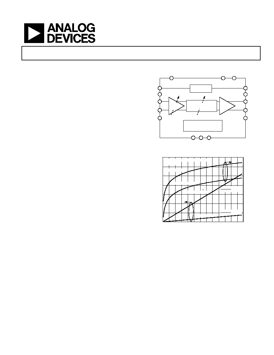
FUNCTIONAL BLOCK DIAGRAM
INHI
INLO
OPHI
OPLO
VCCO
OCOM
ICOM
VOCM
PWUP
VCCO
OCOM
VCCI
ICOM
BIAS CELL
SHIFT REGISTER
AND LATCHES
PRE
AMP
TRANSCONDUCTANCE
OUTPUT
AMP
11
6
1
16
4
14
13
12
5
9
8
3
2
10
7
15
DATA CLCK LTCH
AD8370
03692-
0-
001
Figure 1.
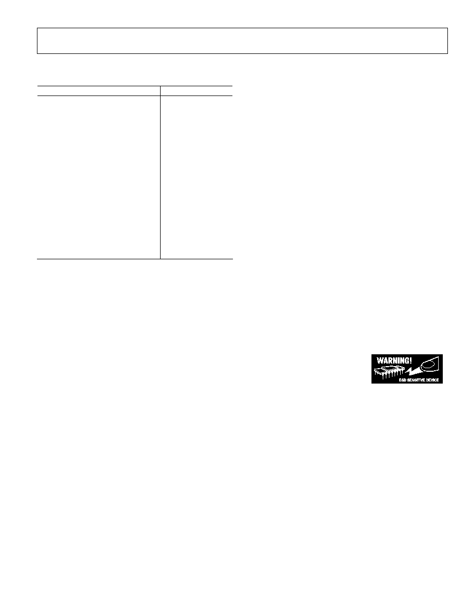
0
10
20
30
40
50
60
70
≠30
≠20
≠10
0
10
20
30
40
VOLTAGE GAIN (
d
B)
VOLTAGE GAIN (
V
/V)
0
10
20
30
40
60
100
50
70
80
90
110 120 130
GAIN CODE
03692-0-003
CODE = LAST 7 BITS OF GAIN CODE
(NO MSB)
HIGH GAIN MODE
HIGH GAIN MODE
LOW GAIN MODE
LOW GAIN MODE
GAIN
CODE
0.409
GAIN
CODE
0.059
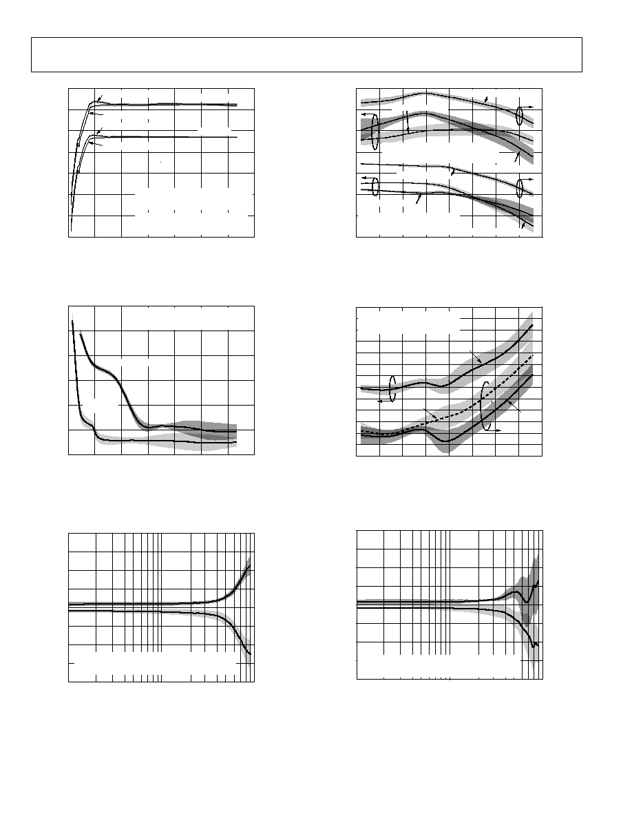
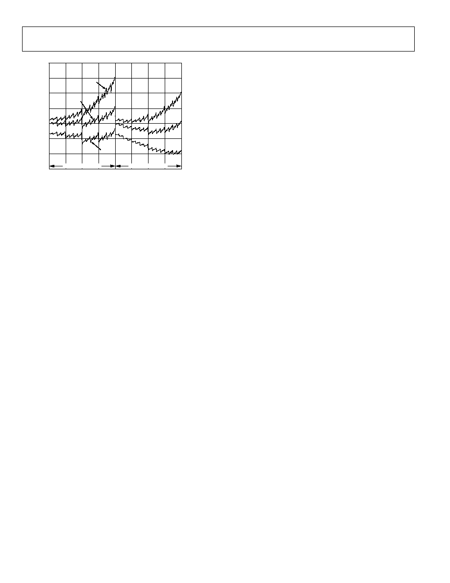
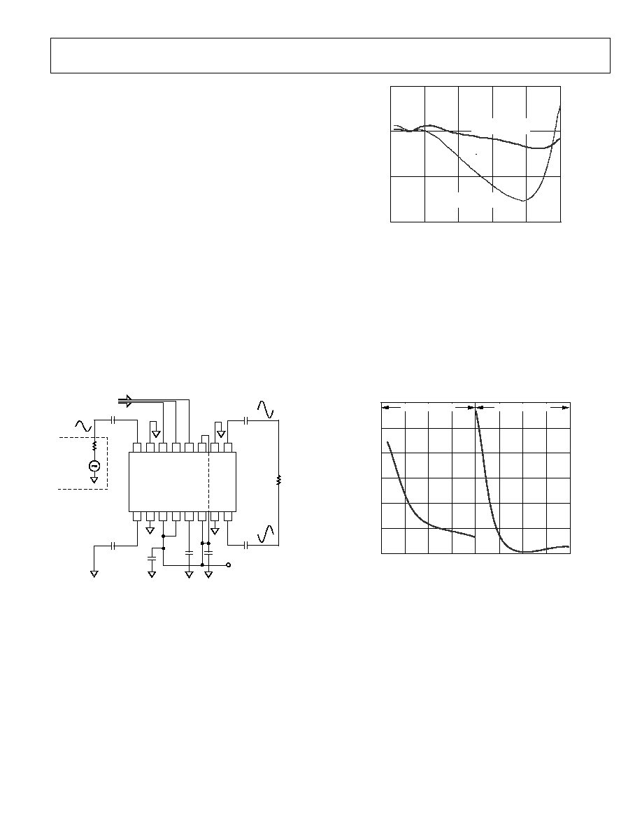
Figure 2. Gain vs. Gain Code at 70 MHz
Gain control of the AD8370 is through a serial 8-bit gain control
word. The MSB selects between the two gain ranges, and the
remaining 7 bits adjust the overall gain in precise linear gain steps.
Fabricated on the ADI high speed XFCB process, the high band-
width of the AD8370 provides high frequency and low distortion.
The quiescent current of the AD8370 is 78 mA typically. The
AD8370 amplifier comes in a compact, thermally enhanced
16-lead TSSOP package and operates over the temperature
range of -40∞C to +85∞C.

AD8370
Rev. 0 | Page 2 of 28
TABLE OF CONTENTS
Specifications..................................................................................... 3
Absolute Maximum Ratings............................................................ 5
ESD Caution.................................................................................. 5
Pin Configuration and Functional Descriptions.......................... 6
Typical Performance Characteristics ............................................. 7
Theory of Operation ...................................................................... 13
Block Architecture...................................................................... 13
Preamplifier................................................................................. 13
Transconductance Stage ............................................................ 13
Output Amplifier ........................................................................ 14
Digital Interface and Timing .................................................... 14
Applications..................................................................................... 15
Basic Connections ...................................................................... 15
Gain Codes .................................................................................. 15
Power-Up Feature....................................................................... 15
Choosing between Gain Ranges............................................... 15
Layout and Operating Considerations .................................... 16
Package Considerations............................................................. 17
Single-Ended-to-Differential Conversion............................... 17
DC-Coupled Operation............................................................. 18
ADC Interfacing ......................................................................... 19
3 V Operation ............................................................................. 20
Evaluation Board and Software .................................................... 21
Appendix ......................................................................................... 24
Characterization Equipment..................................................... 24
Composite Waveform Assumption .......................................... 24
Definitions of Selected Parameters .......................................... 24
Outline Dimensions ....................................................................... 28
Ordering Guide .......................................................................... 28
REVISION HISTORY
Revision 0: Initial Version

AD8370
Rev. 0 | Page 3 of 28
SPECIFICATIONS
V
S
= 5 V, T = 25∞C, Z
S
= 200 , Z
L
= 100 at Gain Code HG127, 70 MHz, 1 V p-p differential output, unless otherwise noted.
Table 1.
Parameter
Conditions
Min
Typ
Max
Unit
DYNAMIC PERFORMANCE
-3 dB Bandwidth
V
OUT
< 1 V p-p
750
MHz
Slew Rate
Gain Code HG127, R
L
= 1 k, AD8370 in
Compression
5750
V/ns
Gain Code LG127, RL = 1 k, V
OUT
= 2 V p-p
3500
V/ns
INPUT STAGE
Pins INHI and IHLO
Maximum Input
Gain Code LG2, 1 dB Compression
3.2
V p-p
Input Resistance
Differential
200
Common-Mode Input Range
3.2
V p-p
CMRR
Differential, f = 10 MHz, Gain Code LG127
77
dB
Input Noise Spectral Density
1.9
nV/Hz
GAIN
Maximum Voltage Gain
High Gain Mode
Gain Code = HG127
34
dB
52
Volts/Volt
Low Gain Mode
Gain Code = LG127
17
dB
7.4
Volts/Volt
Minimum Voltage Gain
High Gain Mode
Gain Code = HG1
-8
dB
0.4
Volts/Volt
Low Gain Mode
Gain Code = LG1
-25
dB
0.06
Volts/Volt
Gain Step Size
High Gain Mode
0.408
(Volts/Volt)/Code
Low Gain Mode
0.056
(Volts/Volt)/Code
Gain Temperature Sensitivity
Gain Code = HG127
≠2 mdB/
∞C
Step Response
For 6 dB gain step, settled to 10% of final value
20
ns
OUTPUT INTERFACE
Pins OPHI and OPLO
Output Voltage Swing
R
L
1 k (1 dB compression)
8.4
V p-p
Output Resistance
Differential
95
Output Differential Offset
V
INHI
= V
INLO
, over all gain codes
±60
mV
NOISE/HARMONIC PERFORMANCE
10 MHz
Gain Flatness
Within ±10 MHz of 10 MHz
±0.01
dB
Noise Figure
7.2
dB
Second Harmonic
1
V
OUT
= 2 V p-p
-77
dBc
Third Harmonic
1
V
OUT
= 2 V p-p
-77
dBc
Output IP3
35
dBm
Output 1 dB Compression Point
17
dBm
See footnotes on next page.

AD8370
Rev. 0 | Page 4 of 28
Parameter
Conditions
Min
Typ
Max
Unit
NOISE/HARMONIC PERFORMANCE
(cont.)
70 MHz
Gain Flatness
Within ±10 MHz of 70 MHz
±0.02
dB
Noise Figure
7.2
dB
Second Harmonic
1
V
OUT
= 2 V p-p
-65
dBc
Third Harmonic
1
V
OUT
= 2 V p-p
-62
dBc
Output IP3
35
dBm
Output 1 dB Compression Point
17
dBm
140 MHz
Gain Flatness
Within ±10 MHz of 140 MHz
±0.03
dB
Noise Figure
7.2
dB
Second Harmonic
1
V
OUT
= 2 V p-p
-54
dBc
Third Harmonic
1
V
OUT
= 2 V p-p
-50
dBc
Output IP3
33
dBm
Output 1 dB Compression Point
17
dBm
190 MHz
Gain Flatness
Within ±10 MHz of 240 MHz
±0.03
dB
Noise Figure
7.2
dB
Second Harmonic
1
V
OUT
= 2 V p-p
-43
dBc
Third Harmonic
1
V
OUT
= 2 V p-p
-43
dBc
Output IP3
33
dBm
Output 1 dB Compression Point
17
dBm
240 MHz
Gain Flatness
Within ±10 MHz of 240 MHz
±0.04
dB
Noise Figure
7.4
dB
Second Harmonic
1
V
OUT
= 2 V p-p
≠28
dBc
Third Harmonic
1
V
OUT
= 2 V p-p
≠33
dBc
Output IP3
32
dBm
Output 1 dB Compression Point
17
dBm
380 MHz
Gain Flatness
Within ±10 MHz of 240 MHz
±0.04
dB
Noise Figure
8.1
dB
Output IP3
27
dBm
Output 1 dB Compression Point
14
dBm
POWER-INTERFACE
Supply Voltage
3.0
2
5.5
V
Quiescent Current
3
PWUP High, GC = LG127, R
L
=
, 4 seconds after power-on,
thermal connection made to exposed paddle under device
72.5
79
85.5 mA
vs. Temperature
4
-40∞C T
A
+85∞C
105 mA
Total Supply Current
PWUP High, V
OUT
= 1 V p-p, Z
L
= 100 reactive, GC = LG127
(includes load current)
82
mA
Power Down Current
PWUP Low
3.7
mA
vs. Temperature
4
-40∞C T
A
+85∞C
5 mA
POWER UP INTERFACE
Pin PWUP
Power-Up Threshold
4
Voltage to enable the device
1.8
V
Power-Down Threshold
4
Voltage to disable the device
0.8
V
PWUP Input Bias Current
PWUP = 0 V
400
nA
GAIN CONTROL INTERFACE
Pins CLCK, DATA, and LTCH
V
IH
4
Voltage for a logic high
1.8
V
V
IL
4
Voltage for a logic low
0.8
V
Input Bias Current
900
nA
1
Refer to
for performance into a lighter load.
Figure 20
2
See the
section for more information.
3 V Operation
3
Minimum and maximum specified limits for this parameter are guaranteed by production test.
4
Minimum or maximum specified limit for this parameter is a 6-sigma value and not guaranteed by production test.
AD8370
Rev. 0 | Page 5 of 28
ABSOLUTE MAXIMUM RATINGS
Table 2.
Parameter Rating
Supply Voltage, V
S
5.5 V
PWUP, DATA, CLCK, LTCH
V
S
+ 500 mV
Differential Input Voltage,
V
INHI
≠ V
INLO
2 V
Common-Mode Input Voltage, V
INHI
or
V
INLO,
with respect to ICOM or OCOM
V
S
+ 500 mV
(maximum),
V
ICOM
≠ 500 mV,
V
OCOM
≠ 500 mV
(minimum)
Internal Power Dissipation
575 mW
JA
(Exposed paddle soldered down)
30∞C/W
JA
(Exposed paddle not soldered down)
95∞C/W
JC
(At exposed paddle)
9∞C/W
Maximum Junction Temperature
150∞C
Operating Temperature Range
≠40∞C to +85∞C
Storage Temperature Range
≠65∞C to +150∞C
Lead Temperature Range
(Soldering 60 sec)
235∞C
Stresses above those listed under Absolute Maximum
Ratings may cause permanent damage to the device.
This is a stress rating only; functional operation of the
device at these or any other conditions above those
listed in the operational sections of this specification
is not implied. Exposure to absolute maximum rating
conditions for extended periods may affect device
reliability.
ESD CAUTION
ESD (electrostatic discharge) sensitive device. Electrostatic charges as high as 4000 V readily accumulate on the
human body and test equipment and can discharge without detection. Although this product features
proprietary ESD protection circuitry, permanent damage may occur on devices subjected to high energy
electrostatic discharges. Therefore, proper ESD precautions are recommended to avoid performance
degradation or loss of functionality.
AD8370
Rev. 0 | Page 6 of 28
PIN CONFIGURATION AND FUNCTIONAL DESCRIPTIONS
6
7
8
11
10
9
AD8370
TOP VIEW
(Not to Scale)
2
3
4
5
15
14
1
16
13
12
03692-0-002
INHI
ICOM
VCCI
PWUP
VOCM
VCCO
OCOM
OPHI
OPLO
OCOM
VCCO
LTCH
CLCK
DATA
ICOM
INLO
Figure 3.16-Lead TSSOP
Table 3. Pin Function Descriptions
Pin No.
Mnemonic
Description
1 INHI
Balanced
Differential
Input. Internally biased.
2, 15,
PADDLE
ICOM
Input Common. Connect to a low impedance ground. This node is also connected to the exposed pad on the
bottom of the device.
3
VCCI
Input Positive Supply. 3.0 V to 5.5 V. Should be properly bypassed.
4
PWUP
Power Enable Pin. Device is operational when PWUP is pulled high.
5 VOCM
Common-Mode Output Voltage Pin. The midsupply ((V
VCCO
- V
OCOM
)/2) common-mode voltage is delivered to
this pin for external bypassing for additional common-mode supply decoupling. This can be achieved with a
bypass capacitor to ground. This pin is an output only and is not to be driven externally.
6, 11
VCCO
Output Positive Supply. 3.0 V to 5.5 V. Should be properly bypassed.
7, 10
OCOM
Output Common. Connect to a low impedance ground.
8
OPHI
Balanced Differential Output. Biased to midsupply.
9
OPLO
Balanced Differential Output. Biased to midsupply.
12 LTCH
Serial Data Latch Pin. Serial data is clocked into the shift register via the DATA pin when LTCH is low. Data in
shift register is latched on the next high-going edge.
13
CLCK
Serial Clock Input Pin.
14
DATA
Serial Data Input Pin.
16 INLO
Balanced
Differential
Input. Internally biased.
AD8370
Rev. 0 | Page 7 of 28
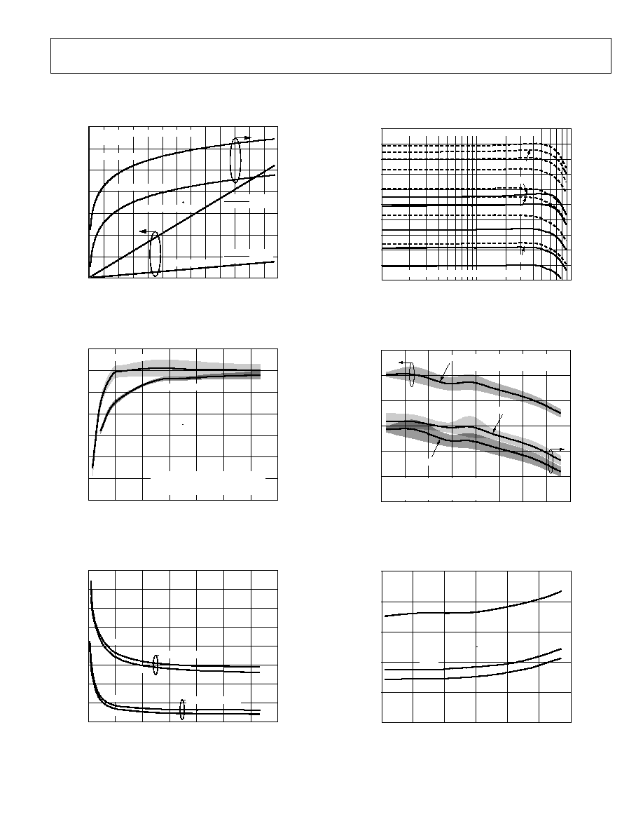
TYPICAL PERFORMANCE CHARACTERISTICS
V
S
= 5 V, Z
S
= 200 , Z
L
= 100 , T = 25∞C, unless otherwise noted.
0
10
20
30
40
50
60
70
≠30
≠20
≠10
0
10
20
30
40
VOLTAGE GAIN (
d
B)
VOLTAGE GAIN (
V
/V)
0
10
20
30
40
60
100
50
70
80
90
110 120 130
GAIN CODE
03692-0-003
CODE = LAST 7 BITS OF GAIN CODE
(NO MSB)
HIGH GAIN MODE
HIGH GAIN MODE
LOW GAIN MODE
LOW GAIN MODE
GAIN
CODE
0.409
GAIN
CODE
0.059
Figure 4. Gain vs. Gain Code at 70 MHz
5
10
15
20
25
30
35
40
OUTPUT IP3 (
d
Bm)
≠5
0
5
10
15
20
25
30
OUTP
UT IP
3
(dBV
rms
)
0
20
40
60
80
100
120
140
GAIN CODE
03692-0-024
HIGH GAIN MODE
LOW GAIN MODE
SHADING INDICATES ±3
FROM THE
MEAN. DATA BASED ON 30 PARTS
FROM TWO BATCH LOTS.
Figure 5. Output Third-Order Intercept vs. Gain Code at 70 MHz
5
10
15
20
25
30
NOIS
E
FIGURE
(dB)
35
40
45
0
20
40
60
80
100
120
140
GAIN CODE
03692-0-012
HIGH GAIN MODE
380 MHz
380 MHz
70 MHz
70 MHz
LOW GAIN MODE
Figure 6. Noise Figure vs. Gain Code at 70 MHz
≠10
≠5
0
5
10
15
20
25
30
35
40
VOLTAGE GAIN (
d
B)
FREQUENCY (MHz)
10
100
1000
03692-0-072
HG77
HG127
LG90
LG9
LG18
LG127
HG102
HG18
LG36
HG51
HG25
HG9
HG3
HIGH GAIN CODES SHOWN WITH DASHED LINES
LOW GAIN CODES SHOWN WITH SOLID LINES
Figure 7. Frequency Response vs. Gain Code
10
15
20
25
30
35
40
OUTP
UT IP
3
(dBm) +2
5∞C
20
25
30
35
40
45
50
OU
TPU
T
IP3 (
d
B
m
)
≠40
∞C
, +
8
5
∞
C
200
150
50
100
0
250
300
350
400
FREQUENCY (MHz)
03692-0-026
+25∞C
UNIT CONVERSION NOTE FOR
100
LOAD: dBVrms = dBm≠10dB
+85∞C
≠40∞C
SHADING INDICATES ±3
FROM THE
MEAN. DATA BASED ON 30 PARTS
FROM TWO BATCH LOTS.
Figure 8. Output Third-Order Intercept vs. Frequency at Maximum Gain
0
5
10
15
20
25
NOIS
E
FIGURE
(dB)
200
300
0
100
400
500
600
FREQUENCY (MHz)
03692-0-011
HG18
HG127
LG127
Figure 9. Noise Figure vs. Frequency at Various Gains
AD8370
Rev. 0 | Page 8 of 28
≠8
≠4
0
4
8
12
16
20
OUTP
UT P
1
dB (dB)
0
20
40
60
80
100
120
140
GAIN CODE
03692-0-028
SHADING INDICATES ±3
FROM THE
MEAN. DATA BASED ON 30 PARTS
FROM TWO BATCH LOTS.
UNIT CONVERSION NOTE:
FOR 100
LOAD: dBVrms = dBm≠10dB
FOR 1k
LOAD: dBVrms = dBm
LOW GAIN MODE
LOW GAIN MODE
HIGH GAIN MODE
100
LOAD
1k
LOAD
HIGH GAIN MODE
Figure 10. Output P1dB vs. Gain Code at 70 MHz
≠85
≠80
≠75
≠70
≠65
≠60
≠55
OUTP
UT IMD (dBc
)
0
20
40
60
80
100
120
140
GAIN CODE
03692-0-027
SHADING INDICATES ±3
FROM THE
MEAN. DATA BASED ON 30 PARTS
FROM TWO BATCH LOTS.
LOW GAIN MODE
HIGH GAIN
MODE
Figure 11. Two-Tone Output IMD3 vs. Gain Code at 70 MHz, R
L
= 1 k,
V
OUT
= 1 V p-p Composite Differential
≠2.0
≠1.5
≠1.0
≠0.5
0
0.5
GAIN E
RROR (dB)
1.0
1.5
2.0
FREQUENCY (MHz)
10
100
1000
03692-0-007
≠40∞C
+85∞C
ERROR AT ≠40∞C AND +85∞C WITH RESPECT TO 25∞C.
SHADING INDICATES ±3
FROM THE MEAN. DATA
BASED ON 30 PARTS FROM ONE BATCH LOT.
Figure 12. Gain Error over Temperature vs. Frequency, R
L
= 100
6
8
10
12
14
16
18
20
OU
TPU
T
P1dB
(
d
B
m
)
≠
40
∞C
, +
85∞C
4
6
8
10
12
14
16
18
OUTPUT P1dB (dBm) +25
∞
C
200
150
50
100
0
250
300
350
400
FREQUENCY (MHz)
03692-0-083
SHADING INDICATES ±3
FROM
THE MEAN. DATA BASED ON 30
PARTS FROM TWO BATCH LOTS.
UNIT CONVERSION NOTE:
RE 100
LOAD: dBVrms = dBm ≠ 10dB
RE 1k
LOAD: dBVrms = dBm
+25∞C, 100
LOAD
+25∞C, 1k
LOAD
+85∞C, 100
LOAD
+85∞C, 1k
LOAD
≠40∞C, 100
LOAD
≠40∞C, 1k
LOAD
Figure 13. Output P1dB vs. Frequency
≠94
≠92
≠88
≠80
≠76
≠72
≠70
≠68
≠84
≠90
≠82
≠78
≠74
≠86
OUTP
UT IMD (dBc
) +2
5
∞
C
≠86
≠84
≠80
≠72
≠68
≠64
≠62
≠60
≠76
≠82
≠74
≠70
≠66
≠78
OUTP
UT IMD (dBc
)
≠
4
0
∞C, +8
5∞C
200
150
50
100
0
250
300
350
400
FREQUENCY (MHz)
03692-0-030
SHADING INDICATES ±3
FROM
THE MEAN. DATA BASED ON 30
PARTS FROM TWO BATCH LOTS.
+25∞C
+85∞C
≠40∞C
Figure 14. Two-Tone Output IMD3 vs. Frequency at Maximum Gain,
R
L
= 1 k, V
OUT
= 1 V p-p Composite Differential
≠2.0
≠1.5
≠1.0
≠0.5
0
0.5
GAIN E
RROR (dB)
1.0
1.5
2.0
FREQUENCY (MHz)
10
100
1000
03692-0-006
ERROR AT ≠40∞C AND +85∞C WITH RESPECT TO 25∞C.
SHADING INDICATES ±3
FROM THE MEAN. DATA
BASED ON 30 PARTS FROM ONE BATCH LOT.
≠40∞C
+85∞C
Figure 15. Gain Error over Temperature vs. Frequency, R
L
= 1 k
AD8370
Rev. 0 | Page 9 of 28
≠90
≠80
≠70
≠60
≠50
≠40
≠30
≠20
≠10
0
HARMONIC DIS
T
ORTION (dBc
)
0
20
40
60
80
100
120
140
GAIN CODE
03692-0-057
HIGH GAIN, R
L
= 1k
LOW GAIN, R
L
= 1k
LOW GAIN, R
L
= 100
HIGH GAIN, R
L
= 100
Figure 16. Second-Order Harmonic Distortion vs. Gain Code at 70 MHz,
V
OUT
= 2 V p-p Differential
1GHz
5MHz
S
22
S
11
0
180
30
330
60
90
270
300
120
240
150
210
03692-0-059
Figure 17. Input and Output Reflection Coefficients, S
11
and S
22
,
Z
O
= 100 Differential
0
50
100
150
200
250
RE
S
I
S
T
ANCE
(
)
≠150
≠100
≠50
0
50
100
RE
ACTANCE
(j
)
0
100
200
300
400
500
600
700
FREQUENCY (MHz)
03692-0-031
16 DIFFERENT GAIN
CODES REPRESENTED
R+jX FORMAT
Figure 18. Input Resistance and Reactance vs. Frequency
≠90
≠80
≠70
≠60
≠50
≠40
≠30
≠20
≠10
0
HARMONIC DIS
T
ORTION (dBc
)
0
20
40
60
80
100
120
140
GAIN CODE
03692-0-036
LOW GAIN R
L
= 100
LOW GAIN R
L
= 1k
HIGH GAIN R
L
= 100
HIGH GAIN R
L
= 1k
Figure 19. Third-Order Harmonic Distortion vs. Gain Code at 70 MHz,
V
OUT
= 2 V p-p Differential
≠90
≠80
≠70
≠60
≠50
≠40
≠30
≠20
≠10
0
HARMONIC DIS
T
ORTION (dBc
)
200
150
50
100
0
250
300
350
400
FREQUENCY (MHz)
03692-0-029
HD
2
R
L
= 100
HD
3
R
L
= 100
HD
3
R
L
= 1k
HD
2
R
L
= 1k
Figure 20. Harmonic Distortion vs. Frequency at Maximum Gain,
V
OUT
= 2 V p-p Composite Differential
0
20
40
60
80
100
120
RE
S
I
S
T
ANCE
(
)
≠40
≠20
0
20
40
60
80
RE
ACTANCE
(j
)
0
100
200
300
400
500
600
700
FREQUENCY (MHz)
03692-0-033
16 DIFFERENT GAIN
CODES REPRESENTED
R+jX FORMAT
Figure 21. Output Resistance and Reactance vs. Frequency
AD8370
Rev. 0 | Page 10 of 28
700
720
740
760
780
800
GROUP DELAY (
p
s)
820
840
860
0
10
20
30
40
60
100
50
70
80
90
110 120 130
GAIN CODE
03692-0-032
HIGH GAIN MODE
LOW GAIN MODE
Figure 22. Group Delay vs. Gain Code at 70 MHz
20
30
40
50
60
70
80
90
100
110
120
P
S
RR (dB)
FREQUENCY (MHz)
1
100
10
1000
03692-0-013
Figure 23. Power Supply Rejection Ratio vs. Frequency at Maximum Gain
≠120
≠100
≠80
≠60
≠40
≠20
0
IS
OLATION (dB)
FREQUENCY (MHz)
10
100
1000
03692-0-009
FORWARD TRANSMISSION, HG0
REVERSE TRANSMISSION, HG127
FORWARD TRANSMISSION, LG0
FORWARD TRANSMISSION, PWUP LOW
Figure 24. Various Forms of Isolation vs. Frequency
600
700
800
900
1000
1100
GROUP DELAY (
p
s)
1200
1300
1400
0
100
200
300
400
500
600
700
800
900
FREQUENCY (MHz)
03692-0-034
R
L
= 1k
R
L
= 100
Figure 25. Group Delay vs. Frequency at Maximum Gain
0
10
20
30
40
50
CMRR (dB)
60
70
80
FREQUENCY (MHz)
10
100
1000
03692-0-005
HG32, HG127
LG32, LG127
Figure 26. Common-Mode Rejection Ratio vs. Frequency
0
2
4
8
10
12
N
O
ISE SPEC
TR
A
L
D
E
N
S
ITY (
n
V/ H
z
)
6
210
310
10
110
410
510
610
FREQUENCY (MHz)
03692-0-010
HG18
HG127
LG127
Figure 27. Input Referred Noise Spectral Density vs.
Frequency at Various Gains
AD8370
Rev. 0 | Page 11 of 28
TIME (2ns/DIV)
VOLTA
GE (
6
00mV/D
I
V)
GND
03692-0-067
DIFFERENTIAL V
IN
DIFFERENTIAL V
OUT
V
OPLO
V
OPHI
Figure 28. DC-Coupled Large Signal Pulse Response
03692-0-068
PWUP (2V/DIV)
TIME (40ns/DIV)
GND
ZERO
INPUT = ≠30dBm, 70MHz 100 AVERAGES
GAIN CODE HG127
DIFFERENTIAL OUTPUT (50mV/DIV)
Figure 29. PWUP Time Domain Response
03692-0-035
LTCH (2V/DIV)
TIME (20ns/DIV)
GND
ZERO
INPUT = ≠30dBm, 70MHz
NO AVERAGING
6dB GAIN STEP (HG36 TO LG127)
DIFFERENTIAL OUTPUT (10mV/DIV)
Figure 30. Gain Step Time Domain Response
TIME (2ns/DIV)
VOLTA
GE (
1
V/D
I
V)
03692-0-069
GND
V
OUT
DIFFERENTIAL
Figure 31. Overdrive Recovery
50
55
60
65
70
75
80
85
S
U
P
P
LY
CURRE
NT (mA)
64
48
16
32
0
80
96
112
128
GAIN CODE
03692-0-014
HIGH GAIN
LOW GAIN
Figure 32. Supply Current vs. Gain Code
0
5
10
15
20
25
30
35
COUNT
50
51
52
53
54
55
GAIN (V/V)
03692-0-073
DATA FROM 136 PARTS
FROM ONE BATCH LOT
MEAN: 51.9
: 0.518
Figure 33. Distribution of Voltage Gain, HG127, 70 MHz, R
L
= 100
AD8370
Rev. 0 | Page 12 of 28
2.40
2.45
2.50
2.55
2.60
2.65
2.70
2.75
V
CM
(V
)
0
96
32
64
0
32
64
96
128
GAIN CODE
03692-0-071
+25∞C
+85∞C
≠40∞C
LOW GAIN MODE
HIGH GAIN MODE
Figure 34. Common-Mode Output Voltage vs. Gain Code at
Various Temperatures
AD8370
Rev. 0 | Page 13 of 28
THEORY OF OPERATION
The AD8370 is a low cost, digitally controlled, fine adjustment
variable gain amplifier that provides both high IP3 and low
noise figure. The AD8370 is fabricated on an ADI proprietary
high performance 25 GHz silicon bipolar process. The ≠3 dB
bandwidth is approximately 750 MHz throughout the variable
gain range. The typical quiescent current of the AD8370 is
78 mA. A power-down feature reduces the current to less than
4 mA. The input impedance is approximately 200 differential,
and the output impedance is approximately 100 differential to
be compatible with saw filters and matching networks used in
intermediate frequency (IF) radio applications. Because there is
no feedback between the input and output and stages within the
amplifier, the input amplifier is isolated from variations in
output loading and from subsequent impedance changes, and
excellent input to output isolation is realized. Excellent distor-
tion performance and wide bandwidth make the AD8370 a
suitable gain control device for modern differential receiver
designs. The AD8370 differential input and output configuration
is ideally suited to fully differential signal chain circuit designs,
although it can be adapted to single-ended system applications,
if required.
BLOCK ARCHITECTURE
The three basic building blocks of the AD8370 are a high/low
gain selectable input preamplifier, a digitally controlled
transconductance (g
m
) block, and a fixed gain output stage.
INHI
INLO
OPHI
OPLO
VCCO
OCOM
ICOM
VOCM
PWUP
VCCO
OCOM
VCCI
ICOM
BIAS CELL
SHIFT REGISTER
AND LATCHES
PRE
AMP
TRANSCONDUCTANCE
OUTPUT
AMP
11
6
1
16
4
14
13
12
5
9
8
3
2
10
7
15
DATA CLCK LTCH
AD8370
03692-
0-
001
Figure 35. Functional Block Diagram
PREAMPLIFIER
There are two selectable input preamplifiers. Selection is made
by the most significant bit (MSB) of the serial gain control data-
word. In the high gain mode, the overall device gain is 7.1 Volts/
Volt (17 dB) above the low gain setting. The two preamplifiers
give the AD8370 the ability to accommodate a wide range of
input amplitudes. The overlap between the two gain ranges
allows the user some flexibility based on noise and distortion
demands. See the Choosing between Gain Ranges section for
more information.
The input impedance is approximately 200 differential,
regardless of which preamplifier is selected. Note that the input
impedance is formed by using active circuit elements and is not
set by passive components. See Figure 36 for a simplified
schematic of the input interface.
1mA
1mA
VCC/2
2k
INHI/INLO
03692-0-018
Figure 36. INHI/INLO Simplified Schematic
TRANSCONDUCTANCE STAGE
The digitally controlled g
m
section has 42 dB of controllable
gain and makes gain the adjustments within each gain range.
The step size resolution ranges from a fine ~ 0.07 dB up to a
coarse 6 dB per bit, depending on the gain code. As shown in
Figure 37, of the 42 dB total range, 28 dB has resolution of
better than 2 dB, and 22 dB has resolution of better than 1 dB.
The curves in Figure 37 show typical input levels that can be
applied to this amplifier at different gain settings. The maxi-
mum input was determined by finding the 1 dB compression or
expansion point of the V
OUT
/V
SOURCE
gain. Note that this is not
V
OUT
/V
IN
. In this way, the change in the input impedance of the
device is also taken into account.
0
0.4
0.8
1.2
1.6
2.0
V
OUT
[
V
peak]
(
V
)
2.4
2.8
3.2
0
0.2
0.4
0.6
0.8
1.0
1.2
1.4
1.6
1.8
V
SOURCE
[V peak] (V)
03692-0-023
HIGH GAIN
0.1dB GAIN
≠5dB GAIN
≠8dB GAIN
12dB
GAIN
6dB
GAIN
<2dB
RES
<2dB
RES
<1dB
RES
<1dB
RES
<0.5dB
RESOLUTION
<0.5dB
RES
≠11dB GAIN
17dB
GAIN
34dB
GAIN
≠25dB GAIN
LOW GAIN
Figure 37. Gain Resolution and Nominal Input and
Output Range over the Gain Range
AD8370
Rev. 0 | Page 14 of 28
OUTPUT AMPLIFIER
Table 4. Serial Programming Timing Parameters
Parameter
Min
Unit
Clock Pulse Width (T
PW
)
25
ns
Clock Period (T
CK
)
50
ns
Setup Time Data vs. Clock (T
DS
)
10
ns
Setup Time Latch vs. Clock (T
ES
)
20
ns
Hold Time Latch vs. Clock (T
EH
)
10
ns
The output impedance is approximately 100 differential and,
like the input preamplifier, this impedance is formed using
active circuit elements. See Figure 38 for a simplified schematic
of the output interface.
VCC/2
740
OPHI/OPLO
03692-0-019
10
µ
A
CLCK/DATA/LTCH/PWUP
03692-0-017
Figure 38. OPHI/OPLO Simplified Circuit
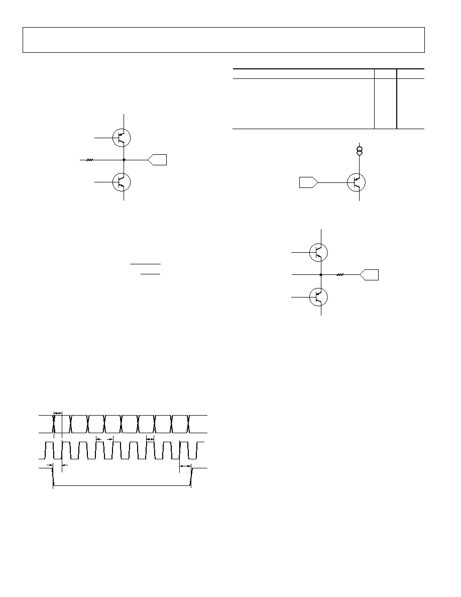
Figure 40. Simplified Circuit for Digital Inputs
The gain of the output amplifier, and thus the AD8370 as a
whole, is load dependent. The following equation can be used to
predict the gain deviation of the AD8370 from that at 100 as
the load is varied:
VCC/2
75
VOCM
03692-0-020
LOAD
R
ion
GainDeviat
98
1
98
.
1
+
=
For example, if R
LOAD
is 1 k, the gain is a factor of 1.80 (5.12 dB)
above that at 100 , all other things being equal. If R
LOAD
is 50 ,
the gain is a factor of 0.669 (3.49 dB) below that at 100 .
Figure 41. Simplified Circuit for VOCM Output
DIGITAL INTERFACE AND TIMING
The digital control port uses a standard TTL interface. The 8-bit
control word is read in a serial fashion when the LTCH pin is
held low. The levels presented to the DATA pin are read on each
rising edge of the CLCK signal. Figure 39 illustrates the timing
diagram for the control interface. Minimum values for timing
parameters are presented in Table 4. Figure 40 is a simplified
schematic of the digital input pins.
DATA
(Pin 14)
CLCK
(Pin 13)
LTCH
(Pin 12)
T
DS
T
ES
T
EH
MSB
MSB-1 MSB-2 MSB-3
LSB
LSB+1
LSB+2
LSB+3
T
CK
T
PW
03692-0-038
Figure 39. Digital Timing Diagram
AD8370
Rev. 0 | Page 15 of 28
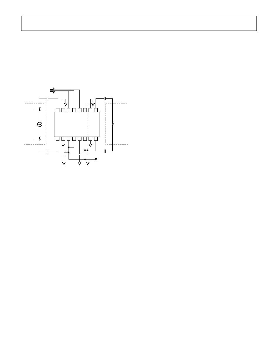
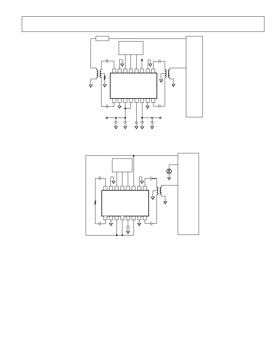
APPLICATIONS
BASIC CONNECTIONS
Figure 42 shows the minimum connections required for basic
operation of the AD8370. Supply voltages between 3.0 V and
5.5 V are allowed. The supply to the VCCO and VCCI pins
should be decoupled with at least one low inductance, surface-
mount ceramic capacitor of 0.1 µF placed as close as possible to
the device.
AD8370
INHI
ICOM
VC
C
I
PW
U
P
VOC
M
VC
C
O
OCOM
OPHI
OPLO
OCOM
V
CCO
LTCH
CLCK
DATA
ICOM
INLO
6
7
8
2
3
5
1
11
10
9
15
14
16
13
12
4
SERIAL CONTROL
INTERFACE
0.1
µ
F
1nF
0.1
µ
F
+V
S
(3.0V TO 5.0V)
1nF
1nF
1nF
1nF
BALANCED
LOAD
R
L
BALANCED
SOURCE
R
S
2
R
S
2
03692-0-037
Figure 42. Basic Connections
The AD8370 is designed to be used in differential signal chains.
Differential signaling allows improved even-order harmonic
cancellation and better common-mode immunity than can be
achieved using a single-ended design. To fully exploit these
benefits, it is necessary to drive and load the device in a
balanced manner. This requires some care to ensure that the
common-mode impedance values presented to each set of
inputs and outputs are balanced. Driving the device with an
unbalanced source can degrade the common-mode rejection
ratio. Loading the device with an unbalanced load can cause
degradation to even-order harmonic distortion and premature
output compression. In general, optimum designs are fully
balanced, although the AD8370 still provides impressive
performance when used in an unbalanced environment.
The AD8370 is a fine adjustment, variable gain amplifier. The
gain control transfer function is linear in voltage gain. On a
decibel scale, this results in the logarithmic transfer functions
indicated in Figure 4. At the low end of the gain transfer
function, the slope is steep, providing a rather coarse control
function. At the high end of the gain control range, the decibel
step size decreases, allowing precise gain adjustment.
GAIN CODES
The AD8370's two gain ranges are referred to as high gain (HG)
and low gain (LG). Within each range, there are 128 possible
gain codes. Therefore, the minimum gain in the low gain range
is given by the nomenclature LG0 whereas the maximum gain
in that range is given by LG127. The same is true for the high
gain range. Both LG0 and HG0 essentially turn off the variable
transconductance stage, and thus no output is available with
these codes. See Figure 24.
The theoretical linear voltage gain can be expressed with respect
to the gain code as
A
V
= GainCode Vernier(1 + (PreGain - 1) MSB)
where:
A
V
is the linear voltage gain.
GainCode is the digital gain control word minus the MSB (the
final 7 bits).
Vernier = 0.055744 V/V
PreGain = 7.079458 V/V
MSB is the most significant bit of the 8-bit gain control word.
The MSB sets the device in either high gain mode (MSB = 1 ) or
low gain mode (MSB = 0).
For example, a gain control word of HG45 (or 10101101 binary)
results in a theoretical linear voltage gain of 17.76 Volts/Volt,
calculated as
45 ◊ 0.055744 ◊ (1 + (7.079458 - 1) ◊ 1)
Increments or decrements in gain within either gain range are
simply a matter of operating on the GainCode. Six ≠dB gain
steps, which are equivalent to doubling or halving the linear
voltage gain, are accomplished by doubling or halving the
GainCode.
When power is first applied to the AD8370, the device is
programmed to code LG0 to avoid overdriving the circuitry
following it.
POWER-UP FEATURE
The power-up feature does not affect the GainCode and the gain
setting is preserved when in power-down mode. Powering
down the AD8370 (bringing PWUP low while power is still
applied to the device) does not erase or change the GainCode
from the AD8370, and the same gain code is in place when the
device is powered up, that is, when PWUP is brought high
again. Removing power from the device all together and
reapplying, however, reprograms to LG0.
CHOOSING BETWEEN GAIN RANGES
There is some overlap between the two gain ranges; users can
choose which one is most appropriate for their needs. When
deciding which preamp to use, consider resolution, noise,
linearity, and spurious-free dynamic range (SFDR). The most
important points to keep in mind are
∑
The low gain range has better gain resolution.
∑
The high gain range has a better noise figure.

AD8370
Rev. 0 | Page 16 of 28
∑
The high gain range has better linearity and SFDR at
higher gains.
∑
Conversely, the low gain range has higher SFDR at lower
gains.
Figure 43 provides a summary of noise, OIP3, IIP3, and SFDR
as a function of device power gain. SFDR is defined as
(
)
S
N
NF
IIP
SFDR
-
-
=
3
3
2
where:
IIP3 is the input third-order intercept point, the output
intercept point in dBm minus the gain in dB.
NF is the noise figure in dB.
N
S
is source resistor noise, ≠174 dBm for a 1 Hz bandwidth at
300
∞
K (27
∞C)
.
In general, N
S
= 10 log
10
(kTB), where k = 1.374 ◊10
-23
, T is the
temperature in degrees Kelvin, and B is the noise bandwidth in
Hertz.
≠30
≠20
≠10
0
10
20
NOIS
E
FIGURE
(dB), OIP
3
AND IIP
3
(dBm)
30
40
50
100
110
120
130
140
150
S
F
DR (dB)
160
170
180
≠30
≠20
≠10
0
10
20
30
40
POWER GAIN (dB)
03692-0-004
SFDR HIGH GAIN
SFDR LOW GAIN
OIP3 HIGH GAIN
OIP3 LOW GAIN
IIP3 LOW GAIN
IIP3 HIGH GAIN
NF HIGH GAIN
NF LOW GAIN
Figure 43. OIP3, IIP3, NF, and SFDR Variation with Gain
As the gain increases, the input amplitude required to deliver
the same output amplitude is reduced. This results in less
distortion at the input stage, and therefore the OIP3 increases.
At some point, the distortion of the input stage becomes small
enough such that the nonlinearity of the output stage becomes
dominant. The OIP3 does not improve significantly as the gain
is increased beyond this point, which explains the knee in the
OIP3 curve. The IIP3 curve has a knee for the same reason;
however, as the gain is increased beyond the knee, the IIP3
starts to decrease rather than increase. This is because in this
region OIP3 is constant, therefore the higher the gain, the lower
the IIP3. The two gain ranges have equal SFDR at approximately
13 dB power gain.
LAYOUT AND OPERATING CONSIDERATIONS
Each input and output pin of the AD8370 presents either a
100 or 50 impedance relative to their respective ac grounds.
To ensure that signal integrity is not seriously impaired by the
printed circuit board, the relevant connection traces should
provide an appropriate characteristic impedance to the ground
plane. This can be achieved through proper layout.
When laying out an RF trace with a controlled impedance,
consider the following:
∑
Space the ground plane to either side of the signal trace at
least 3 line-widths away to ensure that a microstrip
(vertical dielectric) line is formed, rather than a coplanar
(lateral dielectric) waveguide.
∑
Ensure that the width of the microstrip line is constant and
that there are as few discontinuities as possible , such as
component pads, along the length of the line. Width varia-
tions cause impedance discontinuities in the line and may
result in unwanted reflections.
∑
Do not use silkscreen over the signal line because it alters
the line impedance.
∑
Keep the length of the input and output connection lines
as short as possible.
Figure 44 shows the cross section of a PC board and Table 5
show the dimensions that provide a 100 line impedance for
FR-4 board material with
r
= 4.6.
Table 5.
100
50
W
22 mils
13 mils
H
53 mils
8 mils
T 2
mils
2 mils
W
3W
E
R
3W
H
T
03692-0-021
Figure 44. Cross-Sectional View of a PC Board
It possible to approximate a 100 trace on a board designed
with the 50 dimensions above by removing the ground plane
within 3 line-widths of the area directly below the trace.
The AD8370 contains both digital and analog sections. Care
should be taken to ensure that the digital and analog sections
are adequately isolated on the PC board. The use of separate
ground planes for each section connected at only one point via
a ferrite bead inductor ensures that the digital pulses do not
adversely affect the analog section of the AD8370.
AD8370
Rev. 0 | Page 17 of 28
Due to the nature of the AD8370's circuit design, care must be
taken to minimize parasitic capacitance on the input and output.
The AD8370 could become unstable with more than a few pF of
shunt capacitance on each input. Using resistors in series with
input pins is recommended under conditions of high source
capacitance.
High transient and noise levels on the power supply, ground,
and digital inputs can, under some circumstances, reprogram the
AD8370 to an unintended gain code. This further reinforces the
need for proper supply bypassing and decoupling. The user
should also be aware that probing the AD8370 and associated
circuitry during circuit debug may also induce the same effect.
PACKAGE CONSIDERATIONS
The package of the AD8370 is a compact, thermally enhanced
TSSOP 16-lead design. A large exposed paddle on the bottom of
the device provides both a thermal benefit and a low inductance
path to ground for the circuit. To make proper use of this pack-
aging feature, the PCB needs to make contact directly under the
device, connected to an ac/dc common ground reference with
as many vias as possible to lower the inductance and thermal
impedance.
SINGLE-ENDED-TO-DIFFERENTIAL CONVERSION
AD8370
INHI
ICOM
V
CCI
PW
U
P
VOC
M
V
CCO
OCOM
OPHI
OPLO
OCOM
V
CCO
LTCH
CLCK
DATA
ICOM
INLO
6
7
8
2
3
5
1
11
10
9
15
14
16
13
12
4
SERIAL CONTROL
INTERFACE
0.1
µ
F
1nF
0.1
µ
F
+V
S
C
AC
C
AC
C
AC
C
AC
R
L
SINGLE-
ENDED
SOURCE
R
S
03692-0-039
Figure 45. Single-Ended-to-Differential Conversion
The AD8370 is primarily designed for differential signal inter-
facing. The device can be used for single-ended-to-differential
conversion simply by terminating the unused input to ground
using a capacitor as depicted in Figure 45. The ac coupling
capacitors should be selected such that their reactance is negli-
gible at the frequency of operation. For example, using 1 nF
capacitors for C
AC
presents a capacitive reactance of ≠j1.6 on
each input node at 100 MHz. This attenuates the applied input
voltage by 0.003 dB. If 10 pF capacitors had been selected, the
voltage delivered to the input would be reduced by 2.1 dB when
operating with a 200 source impedance.
DIFFERENTIAL BALANCE (dB)
≠1.0
0
≠0.5
0.5
0
100
200
300
400
500
FREQUENCY (MHz)
03692-
0-
040
HIGH GAIN MODE
(GAIN CODE HG255)
LOW GAIN MODE
(GAIN CODE LG127)
Figure 46. Differential Output Balance for a Single-Ended Input Drive at
Maximum Gain (R
L
= 1 k, C
AC
= 10 nF)
Figure 46 illustrates the differential balance at the output for a
single-ended input drive for multiple gain codes. The differential
balance is better than 0.5 dB for signal frequencies less than
250 MHz. Figure 47 depicts the differential balance over the
entire gain range at 10 MHz. The balance is degraded for lower
gain settings because the finite common gain allows some of the
input signal applied to INHI to pass directly through to the
OPLO pin. At higher gain settings, the differential gain dominates
and balance is restored.
0
0.1
0.2
0.3
0.4
0.5
0.6
DIFFE
R
E
N
TIAL BALANCE
(dB)
0
96
32
64
0
32
64
96
128
GAIN CODE
03692-0-041
LOW GAIN MODE
HIGH GAIN MODE
Figure 47. Differential Output Balance at 10 MHz for a Single-Ended Drive vs.
Gain Code (R
L
= 1 k, C
AC
= 10 nF)
Even though the amplifier is no longer being driven in a bal-
anced manner, the distortion performance remains adequate for
most applications. Figure 48 illustrates the harmonic distortion
performance of the circuit in Figure 45 over the entire gain range.
If the amplifier is driven in single-ended mode, the input
impedance varies depending on the value of the resistor used to
terminate the other input as follows:
Rin
SE
= Rin
DIFF
+ R
TERM
where R
TERM
is the termination resistor connected to the other
input.
AD8370
Rev. 0 | Page 18 of 28
≠100
≠90
≠80
≠70
≠60
≠50
≠40
HARM
ONIC DISTORTION (
d
Bc)
0
96
32
64
0
32
64
96
128
GAIN CODE
03692-0-042
HD2
HD2
LOW GAIN MODE
HIGH GAIN MODE
HD3
HD3
Figure 48. Harmonic Distortion of the Circuit in Figure 45
DC-COUPLED OPERATION
AD8370
INHI
ICOM
VC
C
I
PW
U
P
VOC
M
VC
C
O
OCOM
OPHI
OPLO
OCOM
V
CCO
LTCH
CLCK
DATA
ICOM
INLO
6
7
8
2
3
5
1
11
10
9
15
14
16
13
12
4
SERIAL CONTROL
INTERFACE
1nF
1nF
0.1
µ
F
0.1
µ
F
≠2.5V
≠2.5V
0V
0V
+2.5V
R
L
SINGLE-
ENDED
GROUND
REFERENCED
SOURCE
R
S
R
T
03692-0-043
Figure 49. DC Coupling the AD8370. Dual supplies are used to set the input
and output common-mode levels to 0 V.
AD8370
AD8138
I
NHI
IC
OM
VCCI
PWUP
VOCM
VCCO
OC
OM
OPH
I
OPLO
OC
OM
VCCO
LTC
H
CL
CK
DAT
A
IC
OM
IN
LO
6
7
8
2
3
5
1
11
10
9
15
14
16
13
12
4
SERIAL CONTROL
INTERFACE
1nF
1nF
0.1
µ
F
+5V
499
499
100
499
499
100
V
OC
M
V
OCM
V
OCM
+5V
R
L
SINGLE-ENDED GROUND
REFERENCED SOURCE
R
S
R
T
R
T
2
03692-
0-
044
Figure 50. DC Coupling the AD8370. The AD8138 is used as a unity gain level
shifting amplifier to lift the common-mode level of the source to midsupply.
The AD8370 is also a dc accurate variable gain amplifier. The
common-mode dc voltage present at the output pins is internally
set to midsupply using what is essentially a buffered resistive
divider network connected between the positive supply rail and
the common (ground) pins. The input pins are at a slightly
higher dc potential, typically 250 mV to 550 mV above the out-
put pins, depending on gain setting. In a typical single-supply
application, it is necessary to raise the common-mode reference
level of the source and load to roughly midsupply to maintain
symmetric swing and to avoid sinking or sourcing strong bias
currents from the input and output pins. It is possible to use
balanced dual supplies to allow ground referenced source and
load as indicated in Figure 49. By connecting the VOCM pin
and unused input to ground, the input and output common-
mode potentials are forced to virtual ground. This allows direct
coupling of ground referenced source and loads. The initial
differential input offset is typically only a few 100 µV. Over
temperature, the input offset could be as high as a few tens of
mVs. If precise dc accuracy is need over temperature and time, it
may be necessary to periodically measure the input offset and to
apply the necessary opposing offset to the unused differential
input, canceling the resulting output offset.
To address situations where dual supplies are not convenient, a
second option is presented in Figure 50. The AD8138 differential
amplifier is used to translate the common-mode level of the
driving source to midsupply, which allows dc accurate perform-
ance with a ground-referenced source without the need for dual
supplies. The bandwidth of the solution in Figure 50 is limited
by the gain-bandwidth product of the AD8138. The normalized
frequency response of both implementations is shown in Figure 51.
≠10
≠8
≠6
≠4
≠2
0
2
4
6
8
10
N
O
R
M
A
L
IZED
R
ESPON
SE (
d
B
)
1
10
100
1k
10k
100k
1M
10M 100M
1G
FREQUENCY (Hz)
03692-0-045
AD8370 WITH
AD8138 SINGLE
+5V SUPPLY
AD8370
USING DUAL
±2.5V SUPPLY
Figure 51. Normalized Frequency Response of the Two Solutions in
Figure 49 and Figure 50
AD8370
Rev. 0 | Page 19 of 28
ADC INTERFACING
Although the AD8370 is designed to provide a 100 output
source impedance, the device is capable of driving a variety of
loads while maintaining reasonable gain and distortion per-
formance. A common application for the AD8370 is ADC
driving in IF sampling receivers and broadband wide dynamic
range digitizers. The wide gain adjustment range allows the use
of lower resolution ADCs. Figure 52 illustrates a typical ADC
interface network.
AD8370
V
OCM
R
OP
100
C
AC
Z
S
R
IP
03692-
0-
046
V
IN
V
IN
R
OP
C
AC
Z
S
R
IP
R
T
Z
P
Z
IN
ADC
Figure 52. Generic ADC Interface
Many factors need to be considered before defining component
values used in the interface network, such as the desired fre-
quency range of operation, the input swing, and input impedance
of the ADC. AC coupling capacitors, C
AC
, should be used to
block any potential dc offsets present at the AD8370 outputs,
which would otherwise consume the available low-end range of
the ADC. The C
AC
capacitors should be large enough so that
they present negligible reactance over the intended frequency
range of operation. The VOCM pin may serve as an external
reference for ADCs that do not include an on-board reference.
In either case, it is suggested that the VOCM pin be decoupled
to ground through a moderately large bypassing capacitor (1 nF
to 10 nF) to help minimize wideband noise pick-up.
Often it is wise to include input and output parasitic suppression
resistors, R
IP
and R
OP
. Parasitic suppressing resistors help to
prevent resonant effects that occur as a result of internal bond-
wire inductance, pad to substrate capacitance, and stray
capacitance of the printed circuit board trace artwork. If
omitted, undesirable settling characteristics may be observed.
Typically, only 10 to 25 of series resistance is all that is
needed to help dampen resonant effects. Considering that most
ADCs present a relatively high input impedance, very little
signal is lost across the R
IP
and R
OP
series resistors.
Depending on the input impedance presented by the input
system of the ADC, it may be desirable to terminate the ADC
input down to a lower impedance by using a terminating
resistor, R
T
. The high frequency response of the AD8370
exhibits greater peaking when driving very light loads. In
addition, the terminating resistor helps to better define the
input impedance at the ADC input. Any part-to-part variability
of ADC input impedance is reduced when shunting down the
ADC inputs by using a moderate tolerance terminating resistor
(typically a 1% value is acceptable).
After defining reasonable values for coupling capacitors,
suppressing resistors, and the terminating resistor, it is time to
design the intermediate filter network. The example in
Figure 52 suggests a second-order low-pass filter network
comprised of series inductors and a shunt capacitor. The order
and type of filter network used depends on the desired high
frequency rejection required for the ADC interface, as well as
on pass-band ripple and group delay. In some situations, the
signal spectra may already be sufficiently band-limited such
that no additional filter network is necessary, in which case Z
S
would simply be a short and Z
P
would be an open. In other
situations, it may be necessary to have a rather high-order anti-
aliasing filter to help minimize unwanted high frequency
spectra from being aliased down into the first Nyquist zone of
the ADC.
To properly design the filter network, it is necessary to consider
the overall source and load impedance presented by the AD8370
and ADC input, including the additional resistive contribution
of suppression and terminating resistors. The filter design can
then be handled by using a single-ended equivalent circuit as
shown in Figure 53. A variety of references that address filter
synthesis are available. Most provide tables for various filter
types and orders, indicating the normalized inductor and capaci-
tor values for a 1 Hz cutoff frequency and 1 load. After scaling
the normalized prototype element values by the actual desired
cut-off frequency and load impedance, it is simply a matter of
splitting series element reactances in half to realize the final
balanced filter network component values.
V
S
R
S
2
R
S
2
R
L
2
R
L
2
Z
S
2
Z
S
2
Z
P
V
S
R
S
R
L
Z
S
Z
P
SOURCE
LOAD
BALANCED
CONFIGURATION
SINGLE-ENDED
EQUIVALENT
03692-0-047
Figure 53. Single-Ended-to-Differential Network Conversion
As an example, a second-order Butterworth low-pass filter
design is presented where the differential load impedance is
1200 , and the padded source impedance of the AD8370 is
assumed to be 120 . The normalized series inductor value for
the 10-to-1 load-to-source impedance ratio is 0.074H, and the
normalized shunt capacitor is 14.814 F. For a 70 MHz cutoff
frequency, the single-ended equivalent circuit consists of a
200 nH series inductor followed by a 27 pF capacitor. To realize
the balanced equivalent, simply split the 200 nH inductor in
half to realize the network shown in Figure 54.
AD8370
Rev. 0 | Page 20 of 28
V
S
R
S
2
R
S
R
L
R
S
2
R
L
2
R
L
2
27pF
V
S
R
S
= 120
R
L
= 1200
200nH
100nH
100nH
27pF
BALANCED
CONFIGURATION
DE-NORMALIZED
SINGLE-ENDED
EQUIVALENT
V
S
R
S
=
= 0.1
R
L
= 1
L
N
= 0.074H
C
N
14.814F
NORMALIZED
SINGLE-ENDED
EQUIVALENT
= 60
= 60
= 600
= 600
f
C
= 70MHz
f
C
= 1Hz
03692-0-048
Figure 54. Second-Order Butterworth Low-Pass Filter Design Example
A complete design example is shown in Figure 56. The AD8370
is configured for single-ended-to-differential conversion with
the input terminated down to present a single-ended 75 input.
A sixth-order Chebyshev differential filter is used to interface
the output of the AD8370 to the input of the AD9430 170 MSPS
12-bit ADC. The filter minimizes aliasing effects and improves
harmonic distortion performance.
The input of the AD9430 is terminated with a 1.5 k resistor so
that the overall load presented to the filter network is ~1 k.
The variable gain of the AD8370 extends the useable dynamic
range of the ADC. The measured intermodulation distortion of
the combination is presented in Figure 55 at 42 MHz.
≠130
≠120
≠100
≠60
≠40
≠20
≠10
0
≠80
≠110
≠70
≠50
≠30
≠90
dBFS
0
10
20
30
40
50
60
70
FREQUENCY (MHz)
03692-0-050
Figure 55. FFT Plot of Two-Tone Intermodulation Distortion at
42 MHz for the Circuit in Figure 56
In Figure 55, the intermodulation products are comparable to
the noise floor of the ADC. The spurious-free dynamic range of
the combination is better than 66 dB for a 70 MHz measurement
bandwidth.
3 V OPERATION
It is possible to operate the AD8370 at voltages as low as 3 V
with only minor performance degradation. Table 6 gives typical
specifications for operation at 3 V.
Table 6.
Parameter
Typical (70 MHz, R
L
= 100 )
Ouptut IP3
+23.5 dBm
P1dB +12.7
dBm
-3 dB Bandwidth
650 MHz (HG 127)
IMD3
-82 dBc (R
L
= 1 k)
AD8370
INHI
ICOM
V
CCI
PW
U
P
VOC
M
V
CCO
OCOM
OPHI
OPLO
OCOM
V
CCO
LTCH
CLCK
DATA
ICOM
INLO
6
7
8
2
3
5
1
11
10
9
15
14
16
13
12
4
SERIAL CONTROL INTERFACE
FROM 75
Tx-LINE
0.1
µ
F
1nF
0.1
µ
F
+V
S
27pF
68nH
180nH
220nH
39pF
27pF
1.5k
68nH
180nH
220nH
25
25
C
AC
C
AC
100nF
100nF
C
AC
100nF
C
AC
100nF
R
S
120
03692-0-049
V
IN
B
AD9430
V
IN
A
Figure 56. ADC Interface Example
AD8370
Rev. 0 | Page 21 of 28
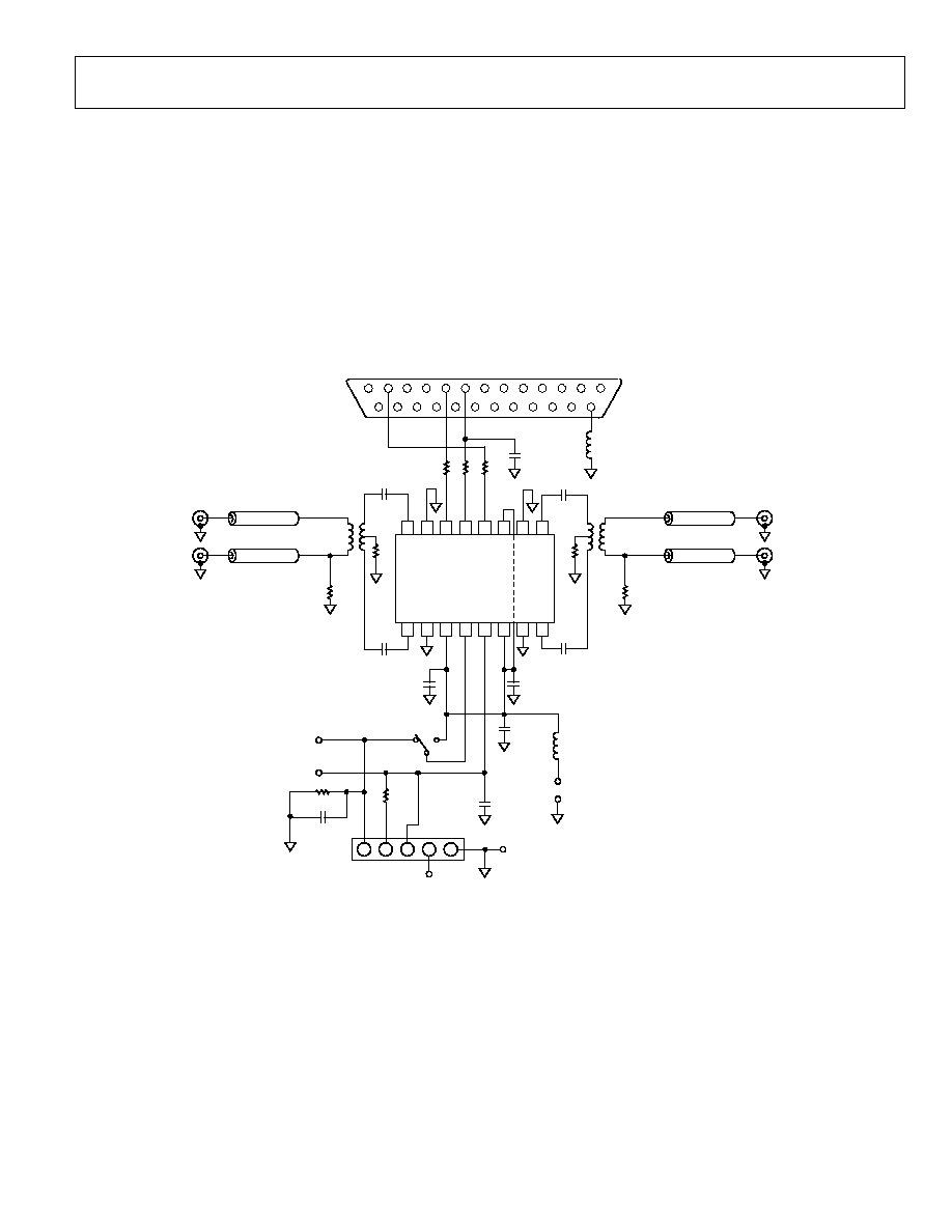
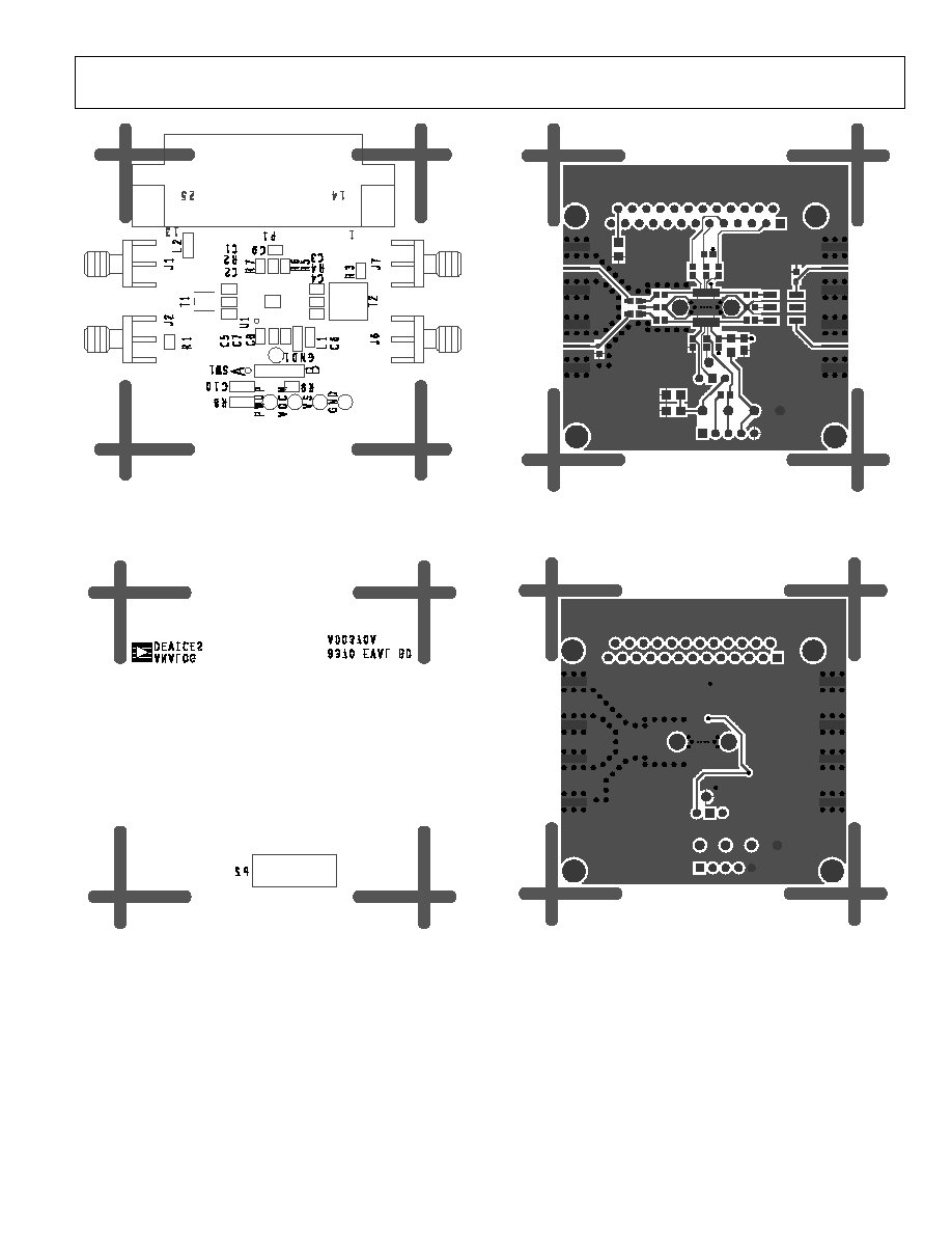
EVALUATION BOARD AND SOFTWARE
The evaluation board allows quick testing of the AD8370 by
using standard 50 test equipment. The schematic is shown in
Figure 57. Transformers T1 and T2 are used to transform 50
source and load impedances to the desired input and output
reference levels. The top and bottom layers are shown in
Figure 61 and Figure 62. The ground plane was removed under
the traces between T1 and pins INHI and INLO to approximate
a 100 characteristic impedance.
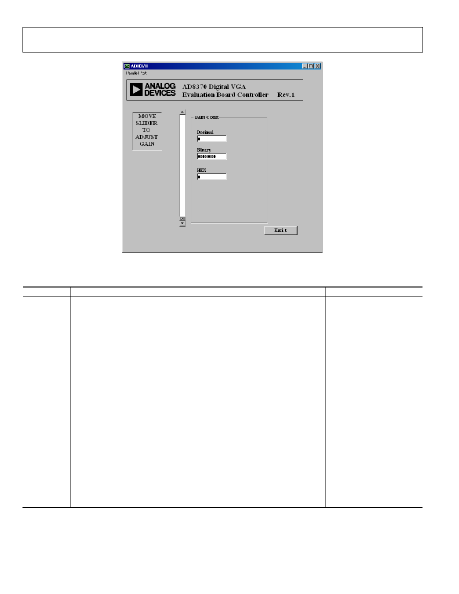
The evaluation board comes with the AD8370 control software
that allows serial gain control from most computers. The
evaluation board is connected via a cable to the parallel port of
the computer. Simply by adjusting the slider bar in the control
software, the gain code is automatically updated to the AD8370.
3
10
12
4
9
8
7
6
11
5
2
13
1
15
22
24
16
21
20
19
18
23
17
14
25
D-SUB 25 PIN MALE
AD8370
INHI
ICOM
V
CCI
PW
U
P
VOC
M
V
CCO
OCOM
OPHI
OPLO
OCOM
V
CCO
LTCH
CLCK
DATA
ICOM
INLO
6
7
8
2
3
5
1
11
10
9
15
14
16
13
12
4
2
3
5
1
4
C8
0.1
µ
F
OUT+
OUT≠
IN+
IN≠
C7
0.1
µ
F
C6
1
µ
F
C5
0.1
µ
F
+V
S
V
S
GND
GND
P2
VOCM
PWUP
C2
C1
T1
1:4
T2
2:1
R2
0
R1
0
R3
0
R4
0
C4
C10 OPEN
R8 49.9
R9
OPEN
SW1
C3
1nF
1nF
1nF
1nF
C9 OPEN
L2*
L1*
R7
1k
R6
1k
R5
1k
03692-0-051
TC4-1W
50
Tx LINE
50
Tx LINE
50
Tx LINE
50
Tx LINE
JTX-2-10T
*
EMI SUPPRESSION FERRITE
HZ1206E601R-00
Figure 57. AD8370 Evaluation Board Schematic
AD8370
Rev. 0 | Page 22 of 28
Figure 58. Evaluation Software
Table 7. AD8370 Evaluation Board Configuration Options
Component Function
Default Condition
VS, GND,
VOCM
Power Interface Vector Pins. Apply supply voltage between VS and GND. The VOCM pin
allows external monitoring of the common-mode input and output bias levels.
Not applicable
SW1, R8, C10,
PWUP
Device Enable. Set to position B to power up the device. When in position A, the PWUP
pin is connected to the PWUP vector pin. The PWUP pin allows external power cycling
of the device. R8 and C10 are provided to allow for proper cable termination.
SW1 = installed
R8 = 49.9 (Size 0805)
C10 = open (Size 0805)
P1, R5, R6, R7,
C9
Serial Control Interface. The evaluation board can be controlled using most PCs.
WindowsÆ based control software is shipped with the evaluation kit. A 25-pin D-sub
connector cable is required to connect the PC to the evaluation board. It may be
necessary to use a capacitor on the clock line, depending on the quality of the PC port
signals. A 1 nF capacitor for C9 is usually sufficient for reducing clock overshoot.
P1 = installed
R5, R6, R7 = 1 k (Size 0603)
C9 = open (Size 0603)
J1, J2, J6, J7
Input and Output Signal Connectors. These SMA connectors provide a convenient way
to interface the evaluation board with 50 test equipment. Typically the device is
evaluated using a single-ended source and load. The source should connect to J1 (IN+),
and the load should connect to J6 (OUT+).
Not applicable
C1, C2, C3, C4
AC Coupling Capacitors. Provide ac coupling of the input and output signals.
C1, C2, C3, C4 = 1 nF (Size 0603)
T1, T2
Impedance Transformers. T1 provides a 50 to 200 impedance transformation. T2
provides a 100 to 50 impedance transformation.
T1 = TC4 -1W (MiniCircuits)
T2 = JTX-2-10T (MiniCircuits)
R1, R2, R3, R4
Single-Ended or Differential. R2 and R4 are used to ground the center tap of the
secondary windings on transformers T1 and T2. R1 and R3 should be used to ground J2
and J7 when used in single ended applications.
R1, R2, R3, R4 = 0 (Size 0603)
C5, C6, C7, C8
L1, L2
Power Supply Decoupling. Nominal supply decoupling consists of a ferrite bead series
inductor followed by a 1 µF capacitor to ground followed by a 0.1 µF capacitor to
ground positioned as close to the device as possible. C7 provides additional decoupling
of the input common-mode voltage. L1 provides high frequency isolation between the
input and output power supply. L2 provides high frequency isolation between the
analog and digital ground.
C6 = 1 µF (Size 0805)
C5, C7, C8 = 0.1 µF (Size 0603)
L1, L2 = HZ1206E601R-00
(Steward, Size 1206)
AD8370
Rev. 0 | Page 23 of 28
03692-
0-
076
Figure 59. Evaluation Board Top Silkscreen
03692-0-078
Figure 60. Evaluation Board Bottom Silkscreen
03692-0-077
Figure 61. Evaluation Board Top
03692-0-079
Figure 62. Evaluation Board Bottom

AD8370
Rev. 0 | Page 24 of 28
APPENDIX
CHARACTERIZATION EQUIPMENT
An Agilent N4441A Balanced Measurement System was used to
obtain the gain, phase, group delay, reverse isolation, CMRR,
and s-parameter information contained in this data sheet. With
the exception for the s-parameter information, T-attenuator
pads were used to match the 50 impedance of this instrument's
ports to the AD8370. An Agilent 4795A Spectrum Analyzer was
used to obtain nonlinear measurements IMD, IP3, and P1dB
through matching baluns and/or attenuator networks. Various
other measurements were taken with setups shown in this
section.
COMPOSITE WAVEFORM ASSUMPTION
The nonlinear two-tone measurements made for this data sheet,
i.e., IMD and IP3, are based on the assumption of a fixed value
composite waveform at the output, generally 1 V p-p. The fre-
quencies of interest dictate the use of RF test equipment, and
because this equipment is generally not designed to work in
units of volts, but rather watts and dBm, an assumption was
made to facilitate equipment setup and operation. Two sinusoidal
tones can be represented as
V
1
= V sin (2f
1
t)
V
2
= V sin (2f
2
t)
The RMS average voltage of one tone is
2
1
)
(
1
2
0
=
dt
V
T
T
1
where T is the period of the waveform. The RMS average
voltage of the two-tone composite signal is
1
)
(
1
2
0
=
+
dt
V
V
T
2
T
1
It can be shown that the average power of this composite
waveform is twice (3 dB) that of the single tone. This also means
that the composite peak-to-peak voltage is twice (6 dB) that of a
single tone. This principle can be used to set correct input
amplitudes from generators scaled in dBm and is correct if the
two tones are of equal amplitude and are reasonably close in
frequency.
DEFINITIONS OF SELECTED PARAMETERS
Common-mode rejection ratio (Figure 26) has been defined for
this characterization effort as
Gain
Mode
Common
Gain
Mode
al
Differenti
where the numerator is the gain into a differential load at the
output due to a differential source at the input, and the
denominator is the gain into a differential-mode load at the
output due to a common-mode source at the input. In terms of
mixed-mode s-parameters, this equates to
SDC21
SDD21
More information on mixed-mode s-parameters can be
obtained in a reference by Bockelman, D.E. and Eisenstadt,
W.R., Combined Differential and Common-Mode Scattering
Parameters: Theory and Simulation. IEEE Transactions on
Microwave Theory and Techniques, v 43, n 7, 1530 (July 1995).
Reverse isolation (Figure 24) is defined as SDD12.
Power supply rejection ratio (PSRR) has been defined as
s
dm
A
A
where A
dm
is the differential mode forward gain (SDD21), and
A
s
is the gain from the power supply pins (VCCI and VCCO,
taken together) to the output (OPLO and OPHI, taken differen-
tially), corrected for impedance mismatch. The following
reference provides more information: Gray, P.R., Hurst, P.J.,
Lewis, S.H. and Meyer, R.G., Analysis and Design of Analog
Integrated Circuits, 4
th
Edition, John Wiley & Sons, Inc., page 422.
AD8370
Rev. 0 | Page 25 of 28
AD8370
I
NHI
IC
OM
V
CCI
PWU
P
VOC
M
V
CCO
OCOM
OPHI
OPLO
OCOM
V
CCO
LTCH
CLCK
DATA
IC
OM
IN
LO
6
7
8
2
3
5
1
11
10
9
15
14
16
13
12
4
1
µ
F
1
µ
F
T1
T2
0
1nF
1nF
1nF
1nF
1nF
1nF
1nF
03692-0-064
MINI-
CIRCUITS
TC4-1W
V
S
5.0V
V
S
5.0V
V
S
5.0V
SERIAL DATA
SOURCE
A
G
ILEN
T 8753D
NE
TW
ORK ANALY
Z
E
R
MINI-
CIRCUITS
TC2-1T
≠22.5dB
PORT 1
PORT 2
Figure 63. PSRR A
dm
Test Setup
AD8370
INHI
ICOM
VCCI
PWUP
VOCM
VCCO
OC
OM
OPH
I
OPLO
OC
OM
VCCO
LTC
H
CL
CK
DAT
A
ICOM
INLO
6
7
8
2
3
5
1
11
10
9
15
14
16
13
12
4
200
1nF
1nF
1nF
1nF
1nF
03692-0-066
SERIAL DATA
SOURCE
AGILENT 8753D
NET
W
O
RK ANAL
YZ
ER
MINI-
CIRCUITS
TC2-1T
PORT 1
PORT 2
BIAS TEE
CONNECTION
TO PORT 1
Figure 64. PSRR A
s
Test Setup

AD8370
Rev. 0 | Page 26 of 28
AD8370
INHI
ICOM
VCCI
PWUP
VOCM
VCCO
OC
OM
OPH
I
OPLO
OC
OM
VCCO
LTC
H
CL
CK
DAT
A
ICOM
INLO
6
7
8
2
3
5
1
11
10
9
15
14
16
13
12
4
1
µ
F
50
INPUT
AUX IN
TEKTRONIX TDS5104
DPO OSCILLOSCOPE
HP8133A
3GHz PULSE
GENERATOR
50
INPUT
50
INPUT
50
INPUT
475
200
52.3
52.3
475
1
µ
F
1nF
1nF
1nF
03692-0-080
V
S
5.0V
2dB
ATTEN
2dB
ATTEN
3dB
ATTEN
3dB
ATTEN
TRIG
OUT
OUT
6dB
SPLITTER
3dB
ATTEN
3dB
ATTEN
6dB
SPLITTER
V
S
5.0V
V
S
5.0V
SERIAL DATA
SOURCE
Figure 65. DC Pulse Response and Overdrive Recovery Test Setup
AD8370
INHI
ICOM
V
CCI
PW
U
P
VOC
M
V
CCO
OCOM
OPHI
OPLO
OCOM
V
CCO
LTCH
CLCK
DATA
ICOM
INLO
6
7
8
2
3
5
1
11
10
9
15
14
16
13
12
4
1
µ
F
475
475
105
1
µ
F
T1
T2
0
1nF
1nF
1nF
1nF
1nF
1nF
1nF
03692-0-081
MINI-
CIRCUITS
TC4-1W
V
S
5.0V
V
S
5.0V
V
S
5.0V
SERIAL DATA
SOURCE
MINI-
CIRCUITS
JTX-2-10T
AGILENT 8648D
SIGNAL
GENERATOR
RF OUT
50
INPUT
50
INPUT
TEKTRONIX
TDS5104 DPO
OSCILLOSCOPE
TEKTRONIX
P6205 ACTIVE
FET PROBE
Figure 66. Gain Step Time Domain Response Test Setup
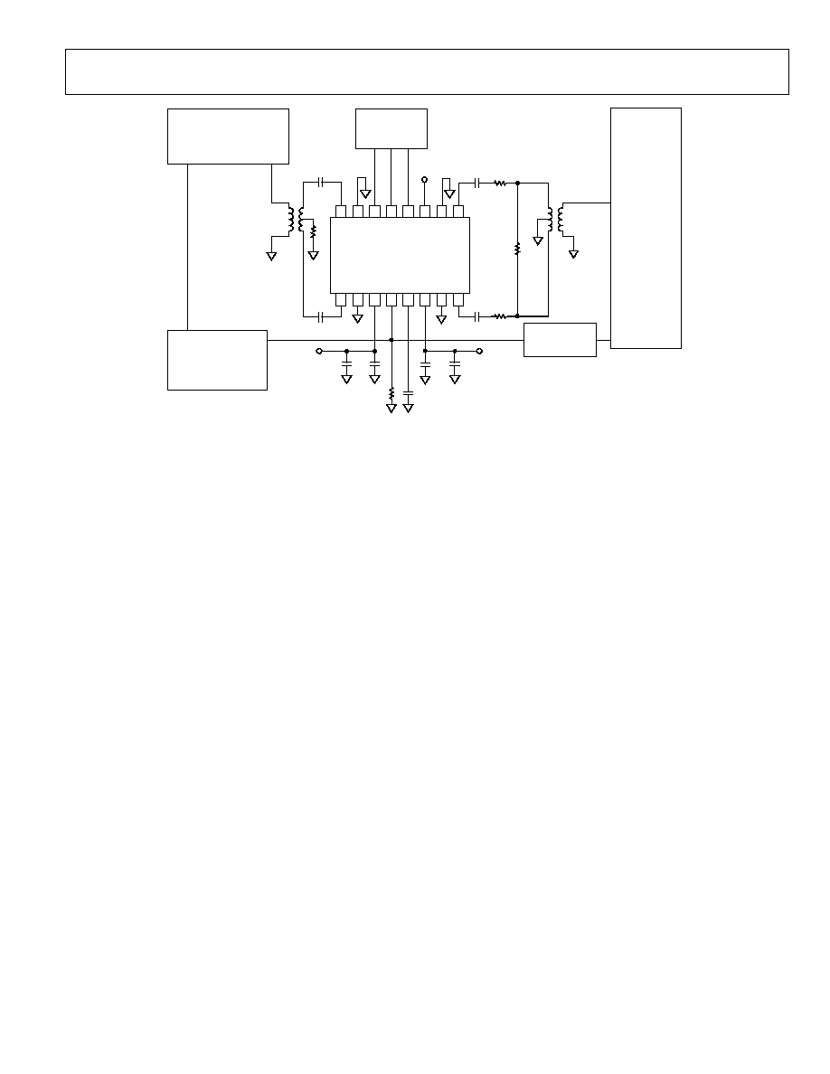
AD8370
Rev. 0 | Page 27 of 28
AD8370
INHI
ICOM
V
CCI
PW
U
P
VOC
M
V
CCO
OCOM
OPHI
OPLO
OCOM
V
CCO
LTCH
CLCK
DATA
ICOM
INLO
6
7
8
2
3
5
1
11
10
9
15
14
16
13
12
4
1
µ
F
52.3
475
475
105
1
µ
F
T1
T2
0
1nF
1nF
1nF
1nF
1nF
1nF
1nF
03692-0-082
MINI-
CIRCUITS
TC4-1W
V
S
5.0V
V
S
5.0V
V
S
5.0V
SERIAL DATA
SOURCE
MINI-
CIRCUITS
JTX-2-10T
AGILENT 8648D
SIGNAL
GENERATOR
RF OUT
AGILENT 33250A
FUNCTION/ARBITRARY
WAVEFORM
GENERATOR
OUTPUT
10MHz IN
10MHz REF OUT
50
INPUT
50
INPUT
TEKTRONIX
TDS5104 DPO
OSCILLOSCOPE
TEKTRONIX
P6205 ACTIVE
FET PROBE
Figure 67. PWUP Response Time Domain Test Setup
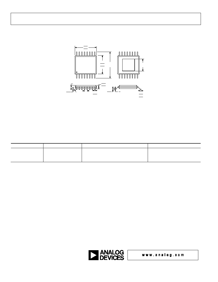
AD8370
Rev. 0 | Page 28 of 28
OUTLINE DIMENSIONS
COMPLIANT TO JEDEC STANDARDS MO-153-ABT
16
9
8
1
EXPOSED
PAD
(Pins Up)
5.10
5.00
4.90
4.50
4.40
4.30
6.40
BSC
3.00
SQ
TOP
VIEW
BOTTOM
VIEW
1.20 MAX
0.15
0.00
1.05
1.00
0.80
0.65
BSC
0.30
0.19
SEATING
PLANE
0.20
0.09
8∞
0∞
0.75
0.60
0.45
Figure 68. 16-Lead TSSOP (RE-16)
ORDERING GUIDE
Model
Temperature
Package Description
Package Option
AD8370ARE
≠40
∞C to +85∞C
16-lead TSSOP, Tube
RE-16
AD8370ARE-REEL7
≠40
∞C to +85∞C
16-lead TSSOP, 7" Reel
RE-16
AD8370-EVAL
Evaluation
Board
© 2004 Analog Devices, Inc. All rights reserved. Trademarks and
registered trademarks are the property of their respective owners.
D03692-0-1/04(0)